Fluke 7260A User manual

For the benefit and convenience of its customers, Fluke
Corporation (Fluke) has reproduced this copy of a manual
which is no longer in production. This manual has not been
edited or updated since the revision date shown on the lower
left hand
corner of
fhe first page. Fluke will not be liable for
any claims, losses or damages of any kind incurred by any
user arising from use of this manual.
NOTE
This manual documents the Model 7260A and its assemblies at the revision levels shown in Appendix 7A.
If your instrument contains assemblies with different revision letters, it will be necessary for you to either
update or backdate this manual. Refer to the supplemental change/errata sheet for newer assemblies, or to
the backdating sheet in Appendix 7A for older assemblies.
7260A
Universal
Counter/Timer
Instruction Manual
P/N 487504
January 1979
Rev. 1 9/80
Rev. 2 2/81
Wg81. John Fluke Mfg. CO., Inc.. all rights reserved Litho in U.S.A

The Fluke Corporation is pleased to hereby grant GIDEP
(Government-Industry Data Exchange Program) permission to reproduce the
manuals listed in the attachment. Permission is granted on the condition
that you legibly reproduce on the copies the legend "Reproduced With
Permission".
It is our understanding from your request dated January 23, 2001,
that the purpose for copying these manuals is to include them in the GIDEP
database, and that the material won't be copied for any other purpose.
Thank you for your cooperation, and for your interest in Fluke.
Sincerely,
Beverly A. Summers
Paralegal
Fluke Corporation
Intellectual Property Law Dept.
Direct: (425) 446-5770 [voice]
(425) 446-5117 [fax]
[email protected] [e-mail]

WARRANTY
Notwithstanding any provision of any agreement the following warranty is exclusive:
The JOHN FLUKE MFG. CO., INC.. warrants each instrument it manufactures to be free from defects in material and
workmanship under normal use and service for the period of 1 year from date of purchase. This warranty extends only
to the original purchaser. This warranty shall not apply to fuses, disposable batteries (rechargeable type batteries are
warranted for 90 days), or any product or parts which have been subject to misuse, neglect, accident, or abnormal
conditions of operations.
In the event of failure of a product covered by this warranty, John Fluke Mfg. Co., Inc., will repair and calibrate an
instrument returned to an authorized Service Facility within 1 year of the original purchase; provided the warrantor’s
examination discloses to its satisfaction that the product was defective. The warrantor may, at its option, replace the
product in lieu of repair. With regard to any instrument returned within 1 year of the original purchase, said repairs or
replacement will be made without charge. If the failure has been caused by misuse, neglect, accident, or abnormal
conditions of operations, repairs will be billed at a nominal cost. In such case, an estimate will be submitted before
work is started, if requested.
THE FOREGOING WARRANTY IS IN LIEU OF ALL OTHER WARRANTIES, EXPRESS OR IMPLIED,
INCLUDING BUT NOT LIMITED TO ANY IMPLIED WARRANTY OF MERCHANTABILITY, FITNESS,
OR ADEQUACY FOR ANY PARTICULAR PURPOSE OR USE. JOHN FLUKE MFG. CO., INC., SHALL
NOT BE LIABLE FOR ANY SPECIAL, INCIDENTAL, OR CONSEQUENTIAL DAMAGES, WHETHER IN
CONTRACT, TORT, OR OTHERWISE.
If any failure occurs, the following steps should be taken:
1. Notify the JOHN FLUKE MFG. CO., INC., or nearest Service facility, giving full details of the difficulty, and
include the model number, type number, and serial number. On receipt of this information, service data, or
shipping instructions will be forwarded to you.
2. On receipt of the shipping instructions, forward the instrument, transportation prepaid. Repairs will be
made at the Service Facility and the instrument returned, transportation prepaid.
SHIPPING TO MANUFACTURER FOR REPAIR OR ADJUSTMENT
All shipments of JOHN FLUKE MFG. CO., INC., instruments should be madevia United Parcel Serviceor”Best Way”’
prepaid. The instrument should be shipped in the original packing carton; or if it is not available, use any suitable
container that is rigid and of adequate size. If asubstitutecontainer is used, the instrumentshould bewrapped in paper
and surrounded with at least four inches of excelsior or similar shock-absorbing material.
CLAIM FOR DAMAGE IN SHIPMENT TO ORIGINAL PURCHASER
The instrument should be thoroughly inspected immediately upon original delivery to purchaser. All material in the
container should bechecked against the enclosed packing list. The manufacturerwill not be responsible for shortages
against the packing sheet unless notified immediately. If the instrument isdamaged in anyway, aclaim should be filed
with the carrier immediately. (To obtain a quotation to repair shipment damage, contact the nearest Fluke Technical
Center.) Final claim and negotiations with the carrier must be completed by the customer.
The JOHN FLUKE MFG. CO., INC, will be happy to answer all applications or use questions, which will enhance your
use of this instrument. Please address your requests or correspondence to: JOHN FLUKE MFG. CO., INC., P.O. BOX
C9090, EVERETT, WASHINGTON 98206, ATTN: Sales Dept. For European Customers: Fluke (Holland) B.V., P.O. Box
5053. 5004 EB, Tilburg, The Netherlands.
‘For European customers, Air Freight prepaid.
John Fluke Mfg. Co., Inc., P.O. Box C9090, Everett, Washington 98208
Rev. 6161
CHAIGE/ERRATAIJ%Q?MATION
1ssmND:l S/81
This change/errata contains information necessary to ensure the
accuracy of the following manual. Enter the corrections in the
manual if either one of the these conditions exist:
l- The revision letter stamped on the indicated PCRis equal
to or higher than that given with each change-
2. No revision letter is indicated at the beginning of each
change-
Title: 7260ADNIVFRSALCOUNTER-TIMER
Print Date: JANUARY1979
Rev- and Date: 2 - 2/81
C/E PACEEFFECIXVITY
PageNo. Print Date
1 7/79
2 7/79
3 7/79
4 7/79
5 7/79
6 7/79
7 9/80
8 9/80
9 9/80
10 9/80
11 S/81
12 S/81

7260ACOUNZER/TIMER
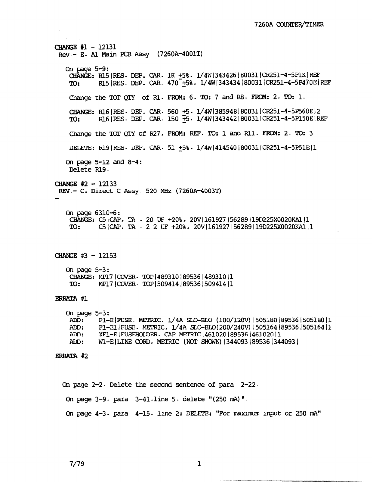
QiANGEYl - 12131
Rev-- E. Al Main PCBAssy (7260A-4001T)
Onpage 5-9:
C~IANGE:RETIRES-DEP.CAR-1~ +5%. 1/4~1343426l800311CR251-4-5~1~I~~~
TO: Rl5IRES- DEP.CAR-470-25%. l/4W13434341&00311CR251-4-5P470ElREF
Changethe TWTQIY of Rl- FROM:6- To: 7 and R&- FRCM:2. To: l-
cHA,bGE:
Rl6IRES- DEP. CAR-560 +5. 1/4W13&594&1800311CR251-4-5P560El2
TO: Rl6IEXES-DIG- CAR-150 25. 1/4W13434421&00311CR251-4-5P150ElREF
Changethe !IWlJQIY of R27. FRCBl:REF. To: 1 and Rll- FROM:2- TO: 3
DEiLEtE:RlgIRJZS-DEP. CAR-51 +5%- 1/4W14145401&0031lCR251-4-5P51E~1
Onpage 5-12 and 8-4:
Delete Rl9-
CHAKEt2 - 12133
REv.- C. Direct C Amy- 520 MHz(7260A-4003T)
Onpage 63106:
CHAGE:C5lcAp.TA - 20 UF+20%.20V1161927l56289119D225X0020KAl
I161927156289119D225X0020KA
To:
C5lCAP.TA - 2 2 UF+20%. 2ov I1
111
CHANGE#3 - 12153
Onpage 5-3:
WE: MP17ICOVER-ToP1489310189536148931011
!Xk MPl71COVER-TOP1509414)&95361509414l1
ERRATAfl
Onpage 5-3:
ADD: Fl-ElFUSE. MEZRIC.l/4A szo-BLO (100/12OV)1505180189536
ADD: Fl-EZLIFUSE-METRIC.l/4A SLC+BLO(200/24OV)1505164l89536
ADD: XFl-EIFUSEHOIDER-CAPMGllRIC1461020189536l46102011
ADD: WI.-EILINECOm. METRIC(m SHOWN)13440931895361344093I
ERRN!A#2
1505180
1505164
Onpage 2-2- Delete the second sentence of para 2-22.
Onpage 3-9- para 3-41-line 5- delete "(250 mA)"-
Onpage 4-3. para 4-15- line 2: DELETE:"For maximuminput of 250 mAI'
7/79 1

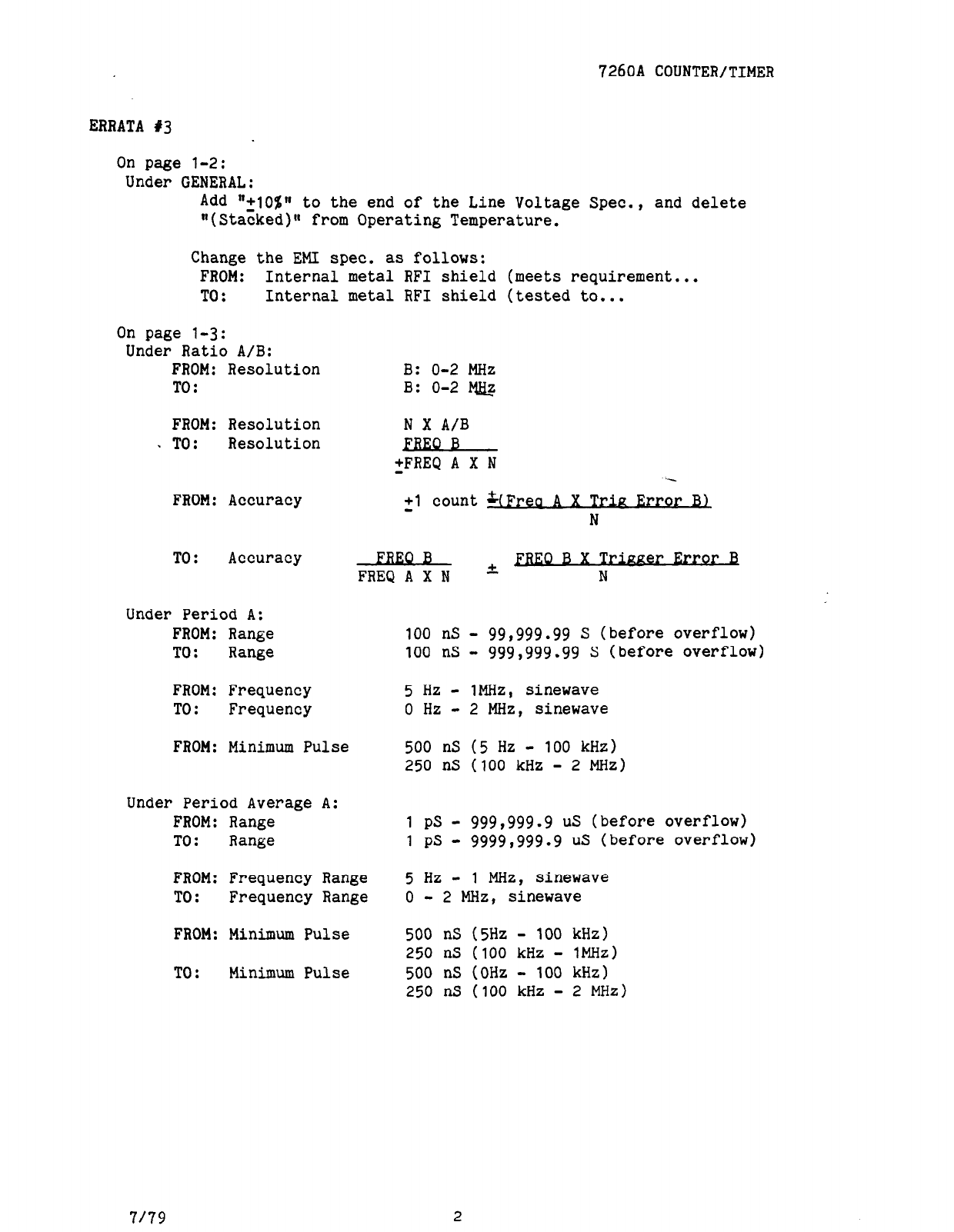
ERRATA
#3
72601 COUNTER/TIMER
On page l-2:
Under GENERAL:
Add
"+lO$w
to the end of the Line Voltage Spec., and delete
"(Stacked)l from Operating Temperature.
Change the EMI spec. as follows:
FROM: Internal metal RF1 shield (meets requirement...
TO: Internal metal RF1 shield (tested to...
On page
l-3:
Under Ratio A/B:
FROM: Resolution
TO:
FROM: Resolution
. TO: Resolution
FROM: Accuracy
TO: Accuracy
Under Period A:
FROM: Range
TO: Range
FROM: Frequency
TO: Frequency
FROM: Minimum Pulse
Under Period Average A:
FROM: Range
TO: Range
FROM: Frequency Range
TO: Frequency Range
FROM: Minimum Pulse
TO: Minimum Pulse
B: O-2 MHz
B: O-2 m
N X A/B
fFREQ A X N .-
+l count +(Frea A X wrror B)
N
FREO B zer Error B
FREQA X N -r- N
100 nS - 99,999.99 S (before overflow)
100
nS - 999,999.99 S (before overflow)
5
Hz - IMHz, sinewave
0 Hz - 2 MHz, sinewave
500
nS (5 Hz -
100
kHz)
250
nS (100 kHz - 2 MHz)
1
ps - 999,999.g US (before overflow)
1 ps - 9999,999.9 US (before overflow)
5
Hz - 1 MHz, sinewave
0 - 2 MHz, sinewave
500
nS (5Hz -
100
kHz)
250
nS
(100
kHz -
1MHz)
500
nS (OHz -
100
kHz)
250
nS
(100
kHz - 2 MHz)
7179
/“.-L__ I ._.._“~I -_
2

7260ACOUNTER/TIMER
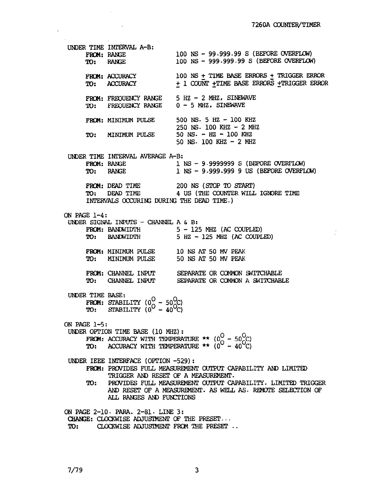
UNDERTIME INl?ERK%A-B:
FX#l:RAKE 100 NS- 99-999-99 S (BEFOREOVERFUW)
TD: RANGE 100 NS- 999-999-99 S (BEFOREOVERFIJX)
FROM:ACCURXY
100 NSf TIMEBASEERRORS2 TRIGGERERROR
m: ACCURACY _+lCouNT+TIMEBASE ERRCRSfTRIGGERERRCR
FRCM:FREC)UEKYRAKE 5 HZ- 2 MHz, SnmiAvE
To: FREGUENCYRANGE0-SMHZ. SINEWAVE
FRCM:MINIMUMPULSE 500 NS- 5 HZ- 100 KHZ
250 NS- 100 KHZ- 2 MHZ
!lD: MINIMUMPULSE 50 NS. - HZ- 100 KHZ
50 NS- 100 KHZ- 2 MHZ
WER TIMEINTERVALAVERAGEA-B:
FRCM: RAIGE
1 NS- 9-9999999S (BEFOREOVERE'LC&J)
To: RAKE 1 NS- 9-999.999 9 US (BEFOREOVERFLx1w)
FROM:DEADTIME 200 NS (STOPTo START)
TO: DEADTIME 4 US (THECOUNTERWILLIGNXETIME
INTERVALSOCCURINGDURINGTHEDEADTIME-)
ONPAGEl-4:
UN)ERSIGNALINPUTS-CHANNEL A& B:
FRal:BANlmIDTH 5 - 125 MHZ(ACCOUPLED)
m: BANlmIDTH 5 HZ- 125 MHZ(ACCOUPLED)
FRCJM:MINIMUMPULSE 10 NSAT50 MVPEAK
To: MINIMUMPULSE 50 NSAT50 MVPEAK
FRCM:CHANNELINPUT SEPARATEORCCXdb0NSWITCHABLE
TO: CHANNELINPUT SEPARATEORCONA %ITCHABLE
UIiDERTIMEBASE:
FR(Xl:STABILITY(0' - SO'C)
To: STABILITYcoo - 40°C)
ONPAGEl-5:
UNDEROl?J!IONTIMEBASE(10 MHZ):
FROM:ACCURACYWITHTEMPERATURE** (0' - 50°C)
To: ACCURACYWITHTEmPERATURE** (0° - 40°C)
UNDERIEEEINTERFACE(OFTION-529) :
FRC+l:PRGVIDESFULLMEASUREMENTGUTPUTCAPABILITYAM) LIMITED
TRIGGERANDRESETOFAMEASUREMENT-
TO: PRGVIDESFULLMEASURENENTOVrPVTCAPABILITY.LIMITEDTRIGGER
ANDRESETOFA
MEASUREMENT.ASWELLAS. REMOTESELECTIONOF
ALL RANGESm FUNCTIONS
ONPAGE2-10. PARA.2-81- LINE 3:
CHAKiE:CLtXXWISEADJUSINEM:OFTHEPRESE;T---
To: CLCCKWISEADJUSIMENTFRQlTHEPRESET--
7/79
3

7260A COUNTER/TIMER
On page 2-11:
The decimal points shown in the top part of Figure 2-12, should
be on the right hand side of each digit, starting with the
second LSD, see Figure d
Figure 1.
Add the following sentence to the end of step 3b;
"for the 7260A PER is more accurate through this functions range
(0 -
2
MHZ)."
On page
3-4,
Figure
3-3,
DELETE: "l/6 MHz,, from the line between clock
select and input A.
On page
3-5,
Figure
3-4,
add an arrowhead showing the input from the
clock select to the main gate count.
On page
3-6:
Line
13,
FROM: . . . will count 10 cycles...
TO: . . . will count
15
cycles...
Line
15,
FROM:
1000.
The display will show
1.000
US.
TO:
1500.
The display will show
1.500 US.
On page
3-7:
Add the following sentence to the end of para. 3-29:
,,unless the effective repetition rate falls below 250 kHz
nominal.,,
On Figure
3-8,
change the name of the
100
MHz waveform TO: MHz
On page
3-11:
DELETE: "(refer to Time Interval Average Logic for an explanation),,
Add a period to the end of the sentence previous to the
information just deleted.
On page
3-12,
Para. 3-49, last line:
CHANGE: . . . a 200 Ns "dead time,, between measurement cycles.
TO: . . . a 4 us "dead time,, .
On page 3-19, Figure 3-17:
CHANGE:5-DIGIT, TO: 6-DIGIT
On page
3-20,
para. 3-90, last sentence:
CHANGE:50 US, TO: 150 mS.
4

7260ACOUNI'EIVTIMER
ONPAGE3-21. PARA-3-94. LINE 11:
7: : -..--. mRTOTHEOPEN-COLLECIYRHIGHIMPEDANCEOPERATIONSTATE-
ONPAGE4-l. TABLE4-1:
ADD: -RIDC-125 MHZ/HP335D
IO-30 DB I
UNDERREOUIREDSPECIFICATIONSIN BOTHPLACES-CHAN3E:UUI. To: 7260A
UNDER RIXOMMENDED TYPE
-E: WAVETEK2001- 'IO: FLUKE6160B
ONPAGE4-5:
PARA.4-29- STEPll- CHANGE:KHZ. To: HZ
PARA.4-29. ENDOFSTEP14. ADD: "(21 COUNT+ TIMEBASEERROR)"
FIGURE4-3:
ADDARECTANGULARBLOCKTOTHELINEB~ENTHEHIGHFREQUENCY
SYNI'HESIZERANDTHERFPROBE-LABELIT :AI%NUATCR"-
ONPAGE4-6:
FIGURE4-4:
ADDARECTAKULAR- LABELED"ATTENUATOR'TOTHELINEBGIWEEN
THEHIGHFREGUEKYSYNTHESIZERANDTHE50 OHMTERM,
PARA.
4-31. STEP4:
czH?uqx:--. OF10 HZAT 100 MVRMS-
To: --I OF10 HZ (AT +l COUNT)AT100 MVRMS-
PARA.4-31. STEP5:
CHANGE:--. OF1000000WITHNJ UNITSANNUNCIATOR
To: --- PF1000000 (+lOOCOUNTS)WITHm UNITSANNUKIATOR.
ADD"(tl COUNT)"TOTHEENDOFSTEP7
ONPAGE4-9:
PARA.4-47. ENDOFSTEP4 ANDSTEP7. ADD"(21 COUNT)"
PARA.4-49- ENDOFSTEP5 - ADD"(+l COUNT)"
PARA.4-49- STEP6. CIIANGE:0 0010: To: O-0200
PARA.4-49- STEP8. CLJANGE:25 MS- TO: 20 MS-
TABLE4-5. ADD"(+l COUNT)"TOTHEDISPLAYHEADING-
PARA.4-51. STEPi:
-E: SLOPECONTROLS- (+) (CHANNELSA ANDB)
TO: SLOPECONI'RCLS- (+) (CHANNELSA) (-) CHANNELB
PARA.4-51. ENDOF STEP4- ADD"(21 COUNT)"-
ONPAGE4-10:
TABLE4-6. ADD:
"(DISPLAYACCURACYIN THIS TABLEDEPENDSONOVERALLINSI'RUMENI
ACCURACY)'I
PARA.4-53. STEpl- CBAKE:'IWIAB - To:IWIAXB
PARA.4-57. STEPl- -E: AC/DC- DC. 10: AC/DC- DC (CHAN-A)
PARA.4-57. STEP9. ADD"t&30 COUNTS)"
7/79
5

7260ACOUNTER/TIMER
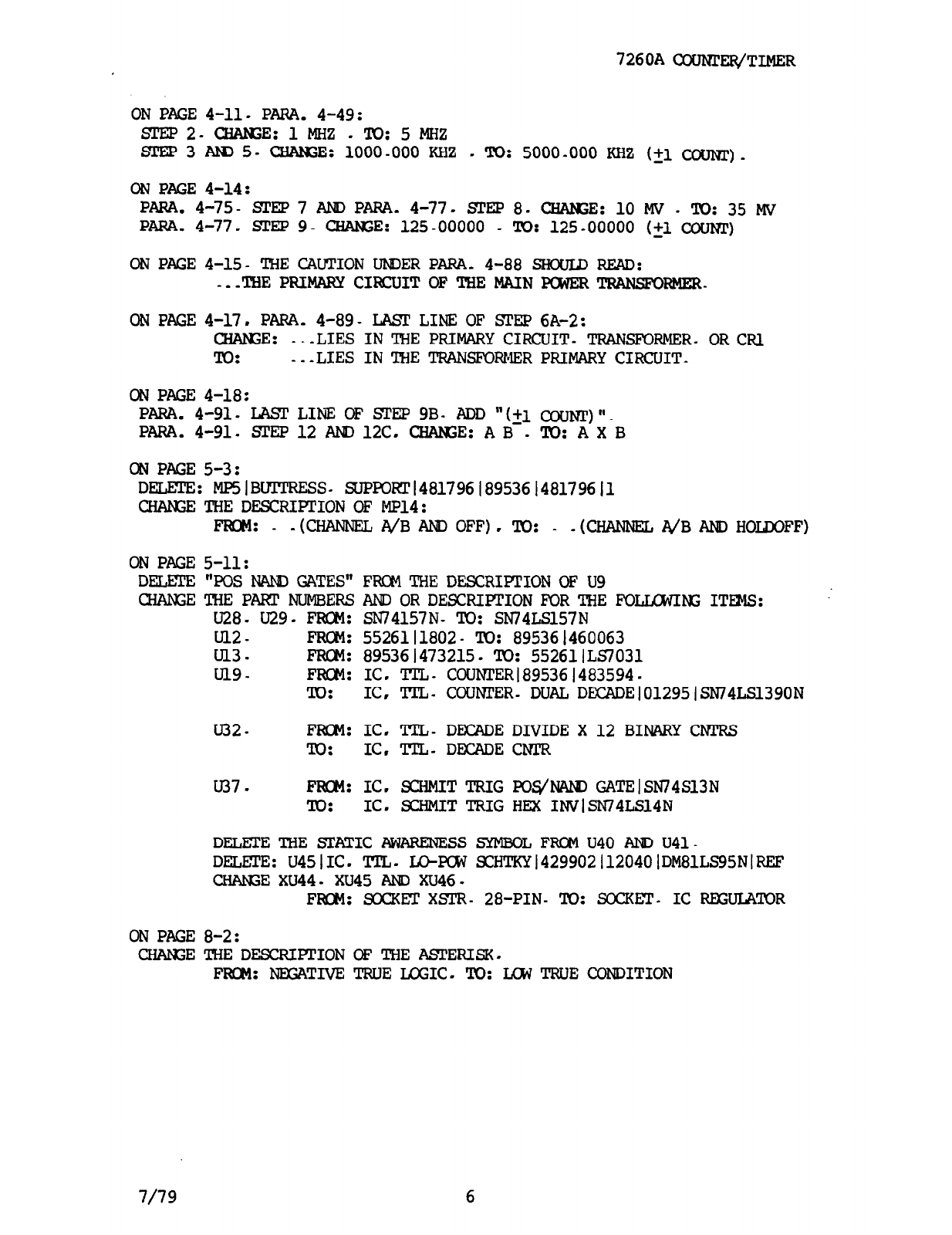
ONPAGE4-11. PARA.4-49:
SI'EP2.CHAWE:lMHZ -To:5MHZ
SI'EF'3 AN35. CHAISE:1000.000 KHZ - To: 5000-000 KHZ(21 COUNT).
ONPAGE4-14:
PARA.4-75. STEP7 ANDPARA.4-77. STEP8. CHAKE: 10 MV - To: 35 MV
PARA.4-77. STEP9. CHANGE:125-00000 - To: 125.00000 (21 COUNT)
ONPAGE4-15. THECAUTIONWER PARA.4-88 SH0UlDREAD:
-. .THEPRIMARYCIRCUITOF THEMAINPWERTRANSF0RMER.
ONPAGE4-17. PARA.4-89. LASTLINE OFSTEP6A-2:
CHAN3E:---LIES IN THEPRIMARYCIRCUIT- TRANSFORMER.ORCRl
To: -- -LIES IN THETRANSF0RMERPRIMARYCIRCUIT-
ONPAGE4-18:
PARA.4-91. LASTLINE 0F STEP9B. ADD"(_+l c~uw)"-
PARA.4-91. STEP12AM)12C. -E: AB . To: AXB
ONPAGE5-3:
DELETE:MP5IBUTI‘RESS.SUPF0RT~481796~89536~481796~1
CHANGETHEDESCRIPTION0F MP14:
FmM: - -(CHANNELA/B ANDOFF). To: - -(CHANNEL
q/B ANDHOLDOFF)
ONPAGE5-11:
DELETE"EQSNAEH)GATES"
CHANGETHEPAFU'NUMBERS
U28. U29.
FROM:
ul2-
ul3. Gi
ul9- FRCM:
TO:
u32- FWM:
To:
u37. FROM:
TO:
FR0MTHEDESCRIFTIONOFU9
ANDORDESCRIFTIONF0RTHEF0LL@dINGITEMS:
SN74157N.To: SN74LS157N
5526111802.To: 895361460063
895361473215.To: 55261lLS7031
IC. TI'L- C0UNTERl895361483594.
IC, TTL- COUNTER-DUALDiKADElOl295lSN74LSl390N
IC. 'I?&- DECADEDIVIDE X 12 BINARYCNI'RS
IC,'ITL-DECADECNTR
IC. SCHMITTRIG F'0S'Ni-WGATEISN74S13N
IC. SCHMITTRIGHEXINVISN74LS14N
DELETETHESTATICAWARENESSSYMBOLFROMU40ANDU41-
DELETE:U45IIC. TTL- LChEWS%TKYl429902112040lDM81LS95NIREF
CHAhKiEXU44. XU45ANDXU46.
FROM:SOCXETXSTR-28-PIN- To: S0CKET.IC REGULA'IQR
ONPAGE8-2:
CHA?ZiETHEDESCRIETION0FTHEASTERISK.
FROM:NEGATIVETRUEL0GIC. To: m TRUECONDITION
7/79

7260ACOUNTER/TIMER
CHANXt4 - 1251s
Rev.-
F- Al Main PCBAssembly (7260A-4001T)
J-K F/F(402743l07263lF9S029DCtl
~137031210129SiC931602l1
On page S-11:
DEZEZE:U7lIC. ECL. EDGE-TRIG-
ADD: XU7JSOCKF11.IC. 16-PIN
Onpage S-3:
ADD: U7lIC. EZL. mE-TRIG-
CHAEE#S- 12555
J-K F/F~402743l07263jF95029DC~1
Rev.- G. Al Main PCSAssembly (7260A-4001T)
=--W
Onpage 5-11:
CHAEE: Ul4IIC. ECL. QUAD.2-INPUT mR GATE15044311072631F95102ll
To: Ul4ILINE RECEIVERASSY.(726OA-4201)1S27218189S36152721811
WE P6 - 12585. 12632. 12786. 12804 i
&V.-
H- Al Main PCHAssy- (7260A-4001T)
On page 5-3:
CHANGE:U44)IC. LINEAR-VOLTAGEREGULA~R1355107112040lLM340T-5l111
To: U44IIC. LIN- ADJ- VOLTREG~'IOR1460410112040lLM317!lb511l1
Changethe T0CQTYof Hl.3. FROM:2. TO: 1
-E: NP9lINSULATOR.XSI'Rl412809l13103143-03-211
!lD: MP~IINSULATOR.XSI'R15344531895361S34453)1
ADD: MP20IINSULATOR.XSI'R1S28611189536152861111
Onpage 5-7:
Add MP20(identical to MP9)between U44and the side of the
heatsink. HF8.
Onpage S-8:
Changethe TOTQIY of CS. FROM:5. TO: 7
ADD: CSOICAP.TA. 10 LJF+20%. 20V13306621562891196D106X0020KAlIREF
ADD: C51ICAP.TA. 10 UF120%. 20v13306621S62891196D106X0020KAllREF
Onpage S-9:
Changethe lVTC!IY of R22. FROM:3. TO:1
Onpage S-10:
DELEZE:R28lRES.COMP.4-7K +S%. 1/4W~148072)011211CB4725~REF
DELJZL'E:R29lRES.CQMP.4-7K 75%. 1/4W11480721011211CT347251REF
Changethe TWI'QTYof R34. F-m: 2- To:. 3
ADD: IIGlIRES- COMP.470 +5%. 1/4W1147983l011211CB4715IREF
ADD: R621RES-MI'L- FILM.-1K +l%. 1/8W11682291916371CMF551001FI1
ADD: R63lRES-VAR-200 +lO%.-l/2W(2757431895361275743(1
ADD: R641RES.MTL- FIL&i: 3-01K +l%. l/8W13126451916371CMF553011FI1
lRESISI'ORNEIWORK.4-7K-+2%. l/8W~484063)89536~484063
I1
ADD: RN7
9/80 7

7260ACOUNTER/TIMER
Onpage 5-12. and 8-4:
Delete all reference of R28and R29-
AddRN7between u13 and56.
AddP61betweenU33 andU38-
The components; C50-
approximatly between
Onpage 8-5. makethe changes
,
C51- F&2- R63and ES4will be added
U44and Tl-
as shownin Figure 2-
1 --I-+ JBl-10
f
CR5 u44 E8
VIN VOUT
ADJ R62
I 1.0K ?Vo
Figure 2-
Onpage 8-6:
Add "ES1470"- between U39-11 and P4-20 node-
01 page 8-7:
Delete all reference of R28. R29and their +5V supply.
Add RN74-7K. to the pins of U22 as follcws:
m-10 to U22-9
RN7-9to U22-7
RN7-8to U22-5
RN7-7to U22-3
FUG-5to U22-13
RN-4 to U22-11
RN7-2to U22-17
RN7-1 to +5V (Ul3-27)
RN-6 is not used
CHAEJGEP7 - 13168- 13323
l&V--
D- Direct Channel C Assy (7260A-4003T)
Onpage 310-6:
Changethe IWI QIY of E?2-FRCM:3- To: 4-
9/80

7260ACOUW.ER/TIMER
Onpage 310-7:
ADD: EUIRES- DEP.CAR-470 25%.
1/4w13434341800311CR251-4-5P470EkEF
-E: (J6IIC. DIG- PEFUPHERIAL
DRIVER-8-PIN DIP13939591120401393959~1
To: u6jIC. DGl!L-DUAL,.3-PIN DIP~393959112040~393959(111
Onpage 310-g/310-10 and 8-14:
U6will be addedbetween U4 ahd U5-
R31will be addedbetween MP2and U4-
QI page
CEIAtGEP8
Rev-- K.
8-15:
Changethe symbol of CR6to a conventional diode (not a
varactor) -
The + symbols for; Cl- C2- C4 & C5 are reversed. please
correct.
Removethe -12V column from the top of the page-
Makethe changesas shownin Figure 3.
4+5v NS 4+5V NS
> P6-9
Z> P6-33
> Fe-8
Iii> =-7
Figure 3- '
- 13967
Al Main PCBAssy- (7260A-4001T)
5-8:
CHAKGE:C16lCAP.MICA. 5000 PF+5%. 500V~181065~72136~DMl9F502J[1
TO: C16ICAP.FIXED-0068 UF-210%.200V1342881l80031175F1RA368l1
Onpage 8-7:
Changethe value of C16. FRCM:5000 PF. To: -0068 UF
ERRATA#4
Onpage 2-7. replace Figure 2-8 with Figure 4.
9/80 9

IDEAL
SIGNAL
SCHM1l-r
TRIGGER
OUTPUT
726014COUNTER/TIMER
NOISE
SPIKES
I
1
SCHMITT
TRIGGER
OUTPUT -
I‘ ’ I
‘I 1 I
II ’ 1
J!( I
XTRA COUNT
NOISE
- -UNCERTAINTY IN
CROSSING TIME
Figure 2-8- Noise and Distortion Effects
Figure 4-
Onpage l-2:
Add the following specification to the bottan of the GENERALcolumn-
PlWlECTIONCLASS Class 1 (As defined in IEZ 348)
CHANGE#9 - 13979- 14089
Rev-- E. Direct Channel C Assy- (7260A-4003T)
Onpage 6310-6:
ChangethTVZQIY of R2. FLUX: 4. To: 6
9/80 10

726015.-TIMER
cfi page 6310-q:
ADD: R321RES-DEP.CAR-470 i5%.
1/4W1343434)800311CR251-4-5P470EIREF
ADD: K331RES-DEP.CAR-470 +5%.
l/4W1343434l800311CR251-4-5P470ElREF
Qnpage 5-3:
(ZHAEE:A5ITIMEBASEPCBASSY-1406918
To: ASITIMEBASEPCBASS- (538660
QI page 5-17/5-18:
CHAKE: A5lTIMEBASE
PCB ASSY.
1406918
FIGURE5-4 (1952B-4OlOT)
To: A5lTIMEBASEPCBASSY-1538660
FIGURE5-4 (722OA-4009)
Replace Table 5-4 with Table 1:
TIMEEASEPCBASSEMBLY
--FIGURE 5-4 (7220A-400gT)
538660
89536
538660
REF
CAP, MINIATURE TRIMMER,
1.5-14
UF, 250V
543520 91293
8091
1
CAP, CER, 22 PF +/-5%, 1OOV
448449 80031 2222-638-10229 1
CAP, CER, 0.01 UF +/-20%, 1OOV
CAP, CER, 0.22 UF +/-202, 50V
CHOKE,6-TURN
PINS, CONTACT(NOT SHOWN)
RES, Ml'L. FILM, 47.5
+/-l%, 1/8W
407361 72982
8121-AlOO-W5R-103M 1
309849 71590
CWjOC224K 1
320911 89536
320911
1
376574 00779
j-87022-1
5
306076 91637 CMF5547R5F 1
RES, COMP,
560 +/-55,
1/0W
115303 01121
RES, COHP,
1K +/-52,
1/8W
153916 01121
RES, COMP, 560 +/-55,
1/8W 115303 01121
RES, COUP, 560 +/-55, l/%W
115303 01121
RES, COMP, 560 +/-55,
1/8W 115303 01121
RES, COUP,
560 +/-52, 1/8W
IC, ECL, DUAL 4-5 INPUT OR/NORGATE
CRYSTAL, QUARTZ
L
BB56
15 5
BB1025 1
BB56
15
REF
Em56 15
REF
BB5615 REF
BB5615 REF
MClologP
11
385732 1
115303 01121
454%7 04713
385732 89536
Table1
E&placeFigure 5-4. with Figure 5:
UI
4
CO
89536
89536
89536
89536
406918
538660
406918
538660
R.
7
fib
::
z
cl
LI
Figure 5-
5/81 11

Onpage 8-U- replace Figure 8-5 with Figure 6:
V s,
(21page 8-5: Figure 6
Add to the Time E3asecircuit; SE36to +5V. makethe char&
as shownin Figure 7-
5/81
Figure 7-
12

7260A
Table of Contents
SECTION
1
2
TITLE PAGE
INTRODUCTION AND SPECIFICATIONS .............................. l-l
I-1.
INTRODUCTION ...................................... ......... I-l
1-4. DESCRlPTlON ................................................. l-l
l-9. SPECIFICATIONS .............................................. l-l
OPERATING INSTRUCTIONS ......................................... 2-1
2-I.
2-3.
2-5.
2-6.
2-8.
2-l I.
2-13.
2-15.
2-17.
2-19.
2-21.
2-23.
2-66.
2-68.
2-72.
2-74.
2-76.
2-78.
2-80.
2-83.
2-85.
2-88.
2-90.
2-92.
2-94.
2-96.
2-98.
2-100.
2-102.
2- 104.
2-106
2-108.
2-I IO.
2-l 12.
2-l 14.
INTRODUCTION ............................................... 2-l
SHIPPING INFORMATION ..................................... 2-l
INSTALLATION ............................................... 2-l
Input Power .................................................. 2-l
Instrument Case Mating ........................................ 2-l
Tilt-Down Bail ................................................ 2-2
Rack Installation .............................................. 2-2
OPERATING FEATURES ....................................... 2-2
OPERATING NOTES ........................................... 2-2
AC Line Connection ........................................... 2-2
Maximum Inputs .............................................. 2-2
Counter /Timer Terminology .................................... 2-5
Function Control .............................................. 2-8
Resolution Control ............................................ 2-8
Separate:Common Control ..................................... 2-9
Attenuation Control ........................................... 2-9
Slope Control ................................................. 2-9
Filter Control ................................................. 2-9
Trigger Level Control .......................................... 2-9
TI Holdoff Control ............................................ 2-10
Display ....................................................... 2-10
Trigger Mode Control .......................................... 2-10
RemoteOperation ............................................. 2-10
i\ccuracy ..................................................... 2-10
Dealing with One Count Error .................................. 2-l I
Reducing Time Base Error ...................................... 2-12
Trigger Error Considerations .................................... 2-l 2
Reducing Errors Due to Noise on the Input Signal ................. 2-12
Summary ..................................................... 2-12
OPERATING DIRECTIONS ..................................... 2-12
Initial Procedure ............................................... 2-12
Frequency Measurements (FREQ A) ............................. 2-12
Counts Per Minute Measurements (CPM XIOOA) .................. 2-13
Frequency Measurements (FREQ C) ............................. 2-13
Ratio Measurement (RATIO A; B) ............................... 2-13
i continued on page ii


7260A
TABLE OF CONTENTS -continued
SECTION TITLE PAGE
5
6
7
7A
6
4-30.
4-32.
4-34.
4-36.
4-38.
4-40.
4-42.
4-44.
4-46.
4-48.
4-50.
4-52.
4-54.
4-56.
4-58.
4-60.
4-62.
4-64.
4-66.
4-68.
4-70.
4-72.
4-74.
4-76.
4-78.
4-79.
4-84.
4-86.
4-92.
Sensitivity Test, Channel B ..................................... 4-6
Time Base Test ................................................ 4-6
Display Test .................................................. 4-7
Frequency A Function Test ..................................... 4-7
Frequency C Function Test ..................................... 4-l
Counts Per Minute Function Test ............................... 407
Ratio A/B Function Test ....................................... 4-7
Period A Function Test ........................................ 4-7
Period Average A Function Test ................................. 4-9
Tl A-B Function Test .......................................... 4-9
Time Interval Average Function Test ............................. 4-9
Totalize A Function Test ....................................... 4-10
Self Check Function Test ....................................... 4-10
Autoranging .................................................. 4-10
Filter Test .................................................... 4-10
External Reference Input Test ................................... 4-1 I
Reference Output Test ......................................... 4-11
Marker Output Test ........................................... 4-l I
Trigger Mode Test ............................................. 4-12
CALIBRATION ................................................ 4-12
Time Base Calibration .......................................... 4-12
Coarse Time Base Adjustment ................................... 4-13
Trigger Level Adjust, Channel A ................................ 4-14
Trigger Level Adjustment, Channel B ............................ 4-14
TROUBLESHOOTING .......................................... 4-14
Introduction .................................................. 4-14
Visual Inspection .............................................. 4-15
Fault Isolation Guide .......................................... 4-15
Troubleshooting Techniques .................................... 4- I8
LIST OF REPLACEABLE PARTS ....................................... 5-l
TABLE OFCONTENTS ......................................... 5-1
5-1. INTRODUCTlON ............................................... 5-2
5-4. HOW TO OBTAIN PARTS ...................................... 5-2
OPTIONS AND ACCESSORIES ........................................ 6-l
TABLE OFCONTENTS ........................................ 6-l
GENERAL INFORMATION ............................................. 7-l
MANUAL CHANGE INFORMATION .................................... 7A-1
SCHEMATIC DIAGRAMS .............................................. 6-1
TABLEOFCONTENTS ........................................ 8-l

7260A
List of Illustrations
FIGURE
l-1.
2-1.
2-2.
2-3.
2-4.
2-5.
2-6.
2-7.
2-8.
2-9.
2-10.
2-l 1.
2-12.
3-l.
3-2.
3-3.
3-4.
3-5.
3-6.
3-7.
3-8.
3-9.
3-10.
3-11.
3-12.
3-13.
3-14.
3-15.
3-16.
3-17.
3-18.
3-19.
4-1.
4-2.
4-3.
4-4.
4-5.
4-6.
4-7.
4-8.
4-9.
4-10.
TITLE PAGE
Frontispiece ...
.................................................................
VII1
Dimensions ................................................. ................. 1-6
Instrument Case Mating ....................................................... 2-1
Front Panel Controls, Connectors and Indicators ................................. 2-2
Rear Panel Controls and Connectors ........................ .................... 2-4
Event Timing ................................................................ 2-5
Time Interval Repetition Rate Versus Time Base ................................. 2-6
Hysteresis Window .......... ................................................. 2-6
Input Coupling ............................................................... 2-6
Noise and Distortion Effect .................................................... 2-7
One Count Error ............................................................. 2-7
Trigger Level ................................................................ 2-8
TI Holdoff .................................................................. 2-10
Decimal Point Placement ...................................................... 2-1 I
Functional Block Diagram ..................................................... 3-2
Frequency Measurements ...................................................... 3-4
Counts Per Minute Measurements .............................................. 3-4
Ratio Measurements .......................................................... 3-5
Period Measurements ......................................................... 3-5
Period Averaging Measurements ................................................ 3-6
Time Interval Measurements ................................................... 3-6
Time Interval Average A B Measurements ....................................... 3-7
Totalize A Gated by B Measurements ........................................... 3-8
SelfCheck ................................................................... 3-9
Input Circuitry ............................................................... 3-10
Time Interval Average Logic ................................................... 3-13
Time Interval Average
A
B Measurements ....................................... 3-14
Resolution 100 Logic .......................................................... 3-16
Clock Select Logic ............................................................ 3-18
Gate Select Logic ............................................................. 3-19
Counter Multiplexer (UI3) ..................................................... 3-19
Gate Indicator Circuits ........................................................ 3-20
RemoteLogic ................................................................ 3-21
Latch Removal ............................................................... 4-2
Line Voltage Selection ........................................................ 4-3
Channel A Sensitivity Test ..................................................... 4-5
Channel B Sensitivity Test ..................................................... 4-6
Time Interval Average Test .................................................... 4-9
External Reference Input Test .................................................. 4-11
Marker Check ............................................................... 4-12
Marker Output Waveforms .................................................... 4-12
Time Base Adjustment Location .............................................. . . 4-13
Maintenance Locator ......................................................... 4-16
v/vi
Table of contents
Other Fluke Cash Counter manuals