Geniatech RS-G2L100&RS-V2L100 Installation manual

Room 02-04, 10/F, Block A, Building 8, Shenzhen International Innovation Valley, Dashi Road,
Nanshan District, Shenzhen, Guangdong, China
96Boards CE2.0 Standard
Development Board Hardware User’s Guide
MODEL:RS-G2L100&RS-V2L100

Room 02-04, 10/F, Block A, Building 8, Shenzhen International Innovation Valley, Dashi Road,
Nanshan District, Shenzhen, Guangdong, China
Contents
1 Introduction ......................................................................................................................................... 1
1.1 Board overview ................................................................................................................................ 2
2. What’s in the Box ............................................................................................................................... 3
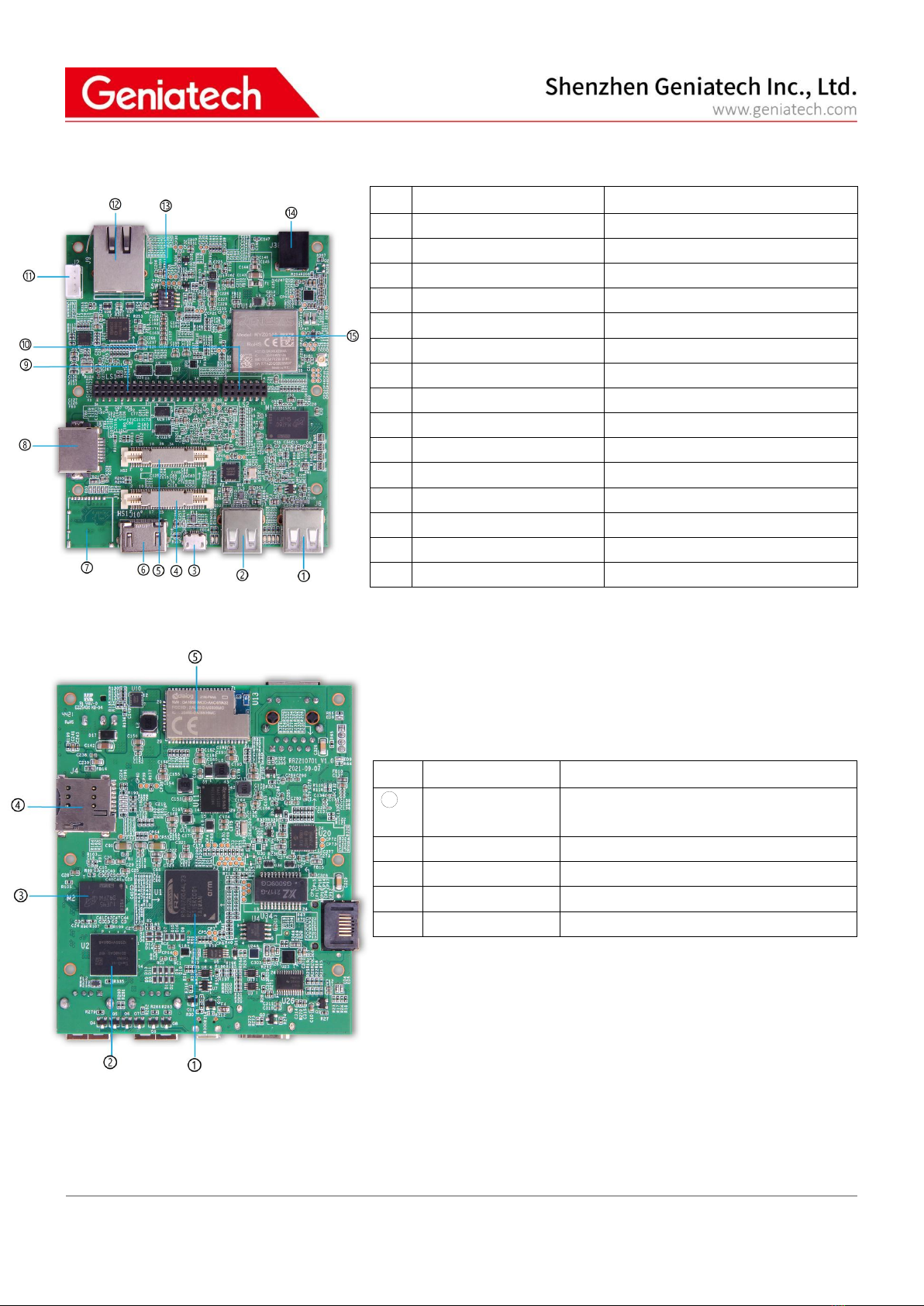
3.RS-G2L100&RS-V2L100 BOARD OVERVIEW ..............................................................................4
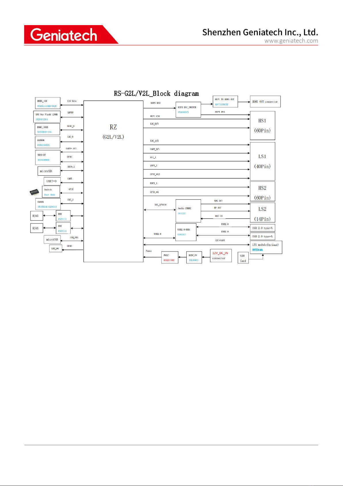
3.1 System Block Diagram .................................................................................................................4
3.2 Processor .......................................................................................................................................4
3.3 Memory ........................................................................................................................................ 4
3.4 MicroSDHC ..................................................................................................................................4
3.5 Display Interface .......................................................................................................................... 5
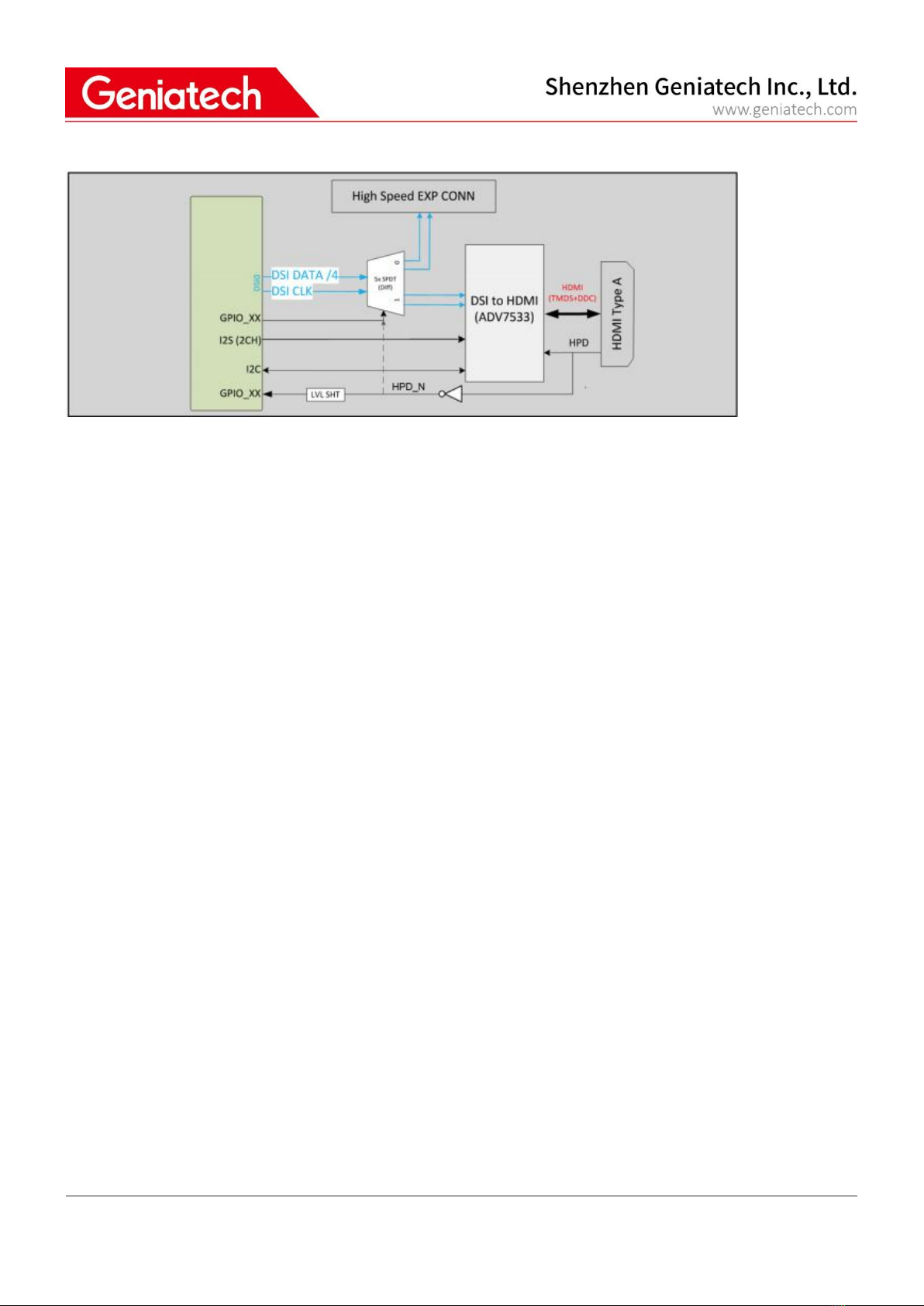
3.5.1 HDMI ..................................................................................................................................... 5
3.5.2 MIPI-DSI ................................................................................................................................5
3.6 Camera Support ............................................................................................................................ 5
3.7 Audio ............................................................................................................................................ 6
3.8 WiFi .............................................................................................................................................. 6
3.9 Bluetooth ...................................................................................................................................... 6
3.10 RGMII ........................................................................................................................................ 6
3.11 USB Port .....................................................................................................................................6
3.11.1 USB-Host ports .....................................................................................................................6
3.11.2 USB-Device port .................................................................................................................. 7
3.12 Debug ......................................................................................................................................... 7
3.12.1 Debug UART ........................................................................................................................7
3.12.2 Debug JTAG ......................................................................................................................... 7
4 40-pin Low Speed(LS) expansion connector ...................................................................................... 7
4.1 UART{0/1} ...................................................................................................................................8
4.2 I2C{0/1} ....................................................................................................................................... 8
4.3 GPIO{A-L} .................................................................................................................................. 8
4.4 SPI 0 ............................................................................................................................................. 8
4.5 I2S .................................................................................................................................................8
5 14-pin Low Speed(LS) expansion connector ...................................................................................... 9
5.1 Speaker ......................................................................................................................................... 9
5.2 Mic ................................................................................................................................................9
5.3 Headset ......................................................................................................................................... 9
6 60-pin High Speed(HS1) expansion connector ................................................................................... 9
6.1 MIPI DSI 2 ................................................................................................................................. 10
6.2 MIPI CSI 0 ..................................................................................................................................11

Room 02-04, 10/F, Block A, Building 8, Shenzhen International Innovation Valley, Dashi Road,
Nanshan District, Shenzhen, Guangdong, China
6.3 I2C{2/3} ..................................................................................................................................... 11
6.4 SD1 ............................................................................................................................................. 11
6.5 Clocks ......................................................................................................................................... 11
6.6 USB ............................................................................................................................................ 11
7 60-pin High Speed(HS2) expansion connector ................................................................................. 11
7.1 SPI 2 ........................................................................................................................................... 12
7.2 GPIO {V,W,X,Y} ....................................................................................................................... 12
8 Power management ........................................................................................................................... 13
8.1 Input Power Supply .................................................................................................................... 13
8.2 12V to 5V@5A Regulator ISL85005 ........................................................................................ 13
8.3 PMIC(RAA215300) ................................................................................................................ 13
9 Status LED’s ......................................................................................................................................13
10 Boot Configuration ..........................................................................................................................14
11 Mechanical specification ................................................................................................................. 15

Room 02-04, 10/F, Block A, Building 8, Shenzhen International Innovation Valley, Dashi Road,
Nanshan District, Shenzhen, Guangdong, China
1
1 Introduction
RS-G2L100&V2L100 Development Board is following 96Boards.CE2.0 standard specifications,based on Renesas artificial
intelligence chip RZ/G2L&RZ/V2L developed by GTC Technology. Renesas RZ/G2L&RZ/V2L chip is a general-purpose SOC
with high performance and lower power consumption designed for industrial human machine interface devices and
AIoT equipment. It adopts 22nm process technology, integrating 2-core arm architecture Cortex-A55 processor and
Cortex-M33 core, 3D Graphics Acceleration Engine Mali-G31 and Video codec H.264. RZ/G2L supports different high
speed interfaces such as MIPI-DSI / MIPI-CSI / USB2.0. RZ/G2L supports Linux systems, and is mainly oriented to the
customized market of Internet of things gateway, POS terminal, industrial control panel, industrial detection, industrial
control box, cloud terminal, vehicle central control and other industries.
This RS-G2L100&V2L100 key features including a high-performance 64-bit Dual-core processor, HDMI out display
support at resolutions up to 1080P , hardware video decode at up to 1080P, up to 4GB of RAM, dual-band 2.4/5.0 GHz
wireless LAN, Bluetooth 4.0, two Gigabit Ethernet, two USB 2.0.
The following table lists its key features:
CHIPSET
Renesas RZ/G2L&RZ/V2L
MARKET AREA
Global
Processor
OS
Yocto(Linux)
CPU
2xCortex-A55 core up to 1.2GHz per core
1x Cortex-M33 core up to 200MHz
DDR4
4GB(4G optional)
EMMC FLASH
8GB eMMC5.1(8-128GB Optional)
NETWORK
Ethernet
2*RJ45, 10/100/1000M
WiFi
WIFI Module 2.4G/5.8G (optional)
Bluetooth
BT4.0(integrated in the WiFi module)
Interface
HDMI Out
*1(up to 1080P30)
USB 2.0
*2
SIM Card slot
*1
USB-OTG
*1
DC IN
*1 (DC-IN Jack)
Connectivity
1x High-Speed Connector1
• intergrade MIPI-CSI/MIPI-DSI/USB/SD1 function
1x High-Speed Connector2
• Support SPI/GPIO
1x Low-Speed Connector1
• UART/I2C/SPI/GPIO/I2S
1x Low-Speed Connector2
•Speak/MIC
Adapter
DC 12V / 3A
Dimensions
100*85mm

Room 02-04, 10/F, Block A, Building 8, Shenzhen International Innovation Valley, Dashi Road,
Nanshan District, Shenzhen, Guangdong, China
2
1.1 Board overview
Top View
Bottom view
2.3.1 Port Description
No.
Name
Description
①
USB2.0 HOST
*1(USB Type-A)
②
USB2.0 HOST
*1(USB Type-A)
③
USB-OTG
*1(Micro-USB Type)
④
High-Speed Connector1
*1(MIPI-CSI/MIPI-DSI/USB/SD1)
⑤
High-Speed Connector2
*1(SPI/GPIO)
⑥
HDMI Connector
*1(up to 1080P30)
⑦
TF Card solt
*1
⑧
Gigabit RJ45 Connector1
*1
⑨
Low-Speed Connector1
*1(UART/I2C/SPI/GPIO/I2S)
⑩
Low-Speed Connector2
*1(Speak/MIC)
⑪
UART Debug connector
*1
⑫
Gigabit RJ45 Connector2
*1
⑬
Model Switch
*1
⑭
DC-IN Jack
*1(12V3A)
⑮
LTE
*1
No.
Name
Description
1
RZ/G2L&RZ/V2
L SOC
*1(2x Cortex-A55 + 1* Cortex-M33)
②
8G eMMC
*1
③
4G DDR4
*1
④
SIM Card solt
*1
⑤
WIFI/BT Module
*1

Room 02-04, 10/F, Block A, Building 8, Shenzhen International Innovation Valley, Dashi Road,
Nanshan District, Shenzhen, Guangdong, China
3
2. What’s in the Box
The box contains one RS-G2L100&RS-V2L100 development board.

Room 02-04, 10/F, Block A, Building 8, Shenzhen International Innovation Valley, Dashi Road,
Nanshan District, Shenzhen, Guangdong, China
4
3.RS-G2L100&RS-V2L100 BOARD OVERVIEW
3.1 System Block Diagram
3.2 Processor
Renesas RZ/G2L&RZ/V2L chip is a general-purpose SOC with high performance and lower power consumption
designed for industrial human machine interface devices and AIoT equipment. It adopts 22nm process technology,
integrating 2-core arm architecture Cortex-A55 processor and Cortex-M33 core, 3D Graphics Acceleration Engine
Mali-G31 and Video codec H.264.
3.3 Memory
The LPDDR4 4GB is a 16bit width bus implementation interfacing directly to the Renesas RZ/G2L&RZ/V2L Processor
build-in LPDDR controller. The maximum DDR clock is 533MHz (1066Mbps).
The eMMC is an 8bit implementation interfacing with Renesas RZ/G2L&RZ/V2L SDC1 interface supporting eMMC 5.0
specifications.
3.4 MicroSDHC
The 96Boards specification calls for microSD port to be on the board. The microSD card is used to flash the board
interfacing with Renesas RZ/G2L&RZ/V2L Dual Core Processor SD2 interface supporting SDIO 3.0 specifications. The size
supports up to 64 GB. The maximum SDIO clock is 200 MHz.

Room 02-04, 10/F, Block A, Building 8, Shenzhen International Innovation Valley, Dashi Road,
Nanshan District, Shenzhen, Guangdong, China
5
3.5 Display Interface
3.5.1 HDMI
The 96Boards specification calls for an HDMI port to be present on the board.
The Renesas RZ/G2L&RZ/V2L doesn’t include a built-in HDMI interface. The Renesas RZ/G2L&RZ/V2L deploys the
built-in MIPI-DSI 4 lanes interface as the source for the HDMI output. A peripheral DSI to HDMI Bridge (U25, Analog
Devices ADV7533) performs this task and it supports a resolution from 480i to 1080p at 30Hz. While the ADV7533
supports automatic input video format timing detection (CEA-861E), an I2C channel from the Renesas RZ/G2L&RZ/V2L
allows the user to configure the operation of this bridge. It is RIIC1_I2C interface from the SoC that connects to the
bridge.
This bridge supports audio as well (meeting the 96Boards requirements to provide audio via HDMI). The Renesas
RZ/G2L100&RZ/V2L100 uses a single bit I2S1 interface from the RZ/G2L&RZ/V2L for this task.
Please note that the 96Boards specification calls for a MIPI-DSI interface to be routed to the High Speed Expansion
connector. Since the RZ/G2L&RZ/V2L has only one MIPI-DSI interface. A muxing device (U24, FSA644UCX) is being use
on the board. Only one interface, HDMI, or the Expansion MIPI-DSI can be active at a given time. The controlling signal
is named
‘P4_1_DSI_SW_SEL’. When this signal is logic low, ‘0’, the MIPI-DSI is routed to the High Speed Expansion connector.
When
‘P4_1_DSI_SW_SEL’ is logic level high, ‘1’, the MIPI-DSI is routed to the DSI-HDMI Bridge. This design
assigned the ‘P4_1_DSI_SW_SEL’ function to P4_1/SCIF2_RXD/MTIOC7B.
3.5.2 MIPI-DSI
The 96Boards specification calls for a MIPI-DSI implementation via the High Speed Expansion Connector.
The Renesas RZ/G2L&RZ/V2L implemented a four-lane MIPI_DSI interface meeting this requirement. More information about
this implementation can be found High speed expansion connector.
3.6 Camera Support
Renesas RZ/G2L&RZ/V2L supports one 4-lane CSI1 port which used to connect high speed expansion connector as per 96boards
standard.

Room 02-04, 10/F, Block A, Building 8, Shenzhen International Innovation Valley, Dashi Road,
Nanshan District, Shenzhen, Guangdong, China
6
3.7 Audio
Renesas RZ/G2L100&RZ/V2L100 supports the requirement of audio codec with MIC IN + Headphone Out 3.5 mm jack
connector.
Renesas RZ/G2L100&RZ/V2L100 supports Automotive Audio Bus interfaces in Master mode with 2 pin connector.
3.8 WiFi
The 96Boards specification calls for WiFi module to be on the board.
Renesas RZ/G2L100&RZ/V2L100 supports Wi-Fi (802.11 a/b/g/n, 2.4GHz) over DA16600MOD-AAE module.
Wi-Fi will be mainly used for cloud connectivity.
The WiFi module is interfacing with RZ/G2L&RZ/V2L Processor QSPI1 interface .
Module is certified with PCB trace antenna.
3.9 Bluetooth
The 96Boards specification calls for bluetooth to be on the board.
Renesas RZ/G2L100&RZ/V2L100 supports Bluetooth 5.2 over DA16600MOD-AAE module.
Bluetooth is used for Audio streaming and BLE sensor communication.
UART communication is used to transfer data between processor and connected Bluetooth device.
UART interface is used for Audio streaming over Bluetooth.
BLE is also supported in the Module.
3.10 RGMII
Renesas RZ/G2L100&RZ/V2L100 supports two 1Gbps Ethernet connection.
Single chip 10/100/1000 Mbps Ethernet Transceiver Suitable for IEEE 802.3 Applications.
Programmable LED Outputs for Link, Activity and Speed.
Power-Down and Power-Saving Modes
3.11 USB Port
3.11.1 USB-Host ports
The 96Boards specification calls for three USB host ports.

Room 02-04, 10/F, Block A, Building 8, Shenzhen International Innovation Valley, Dashi Road,
Nanshan District, Shenzhen, Guangdong, China
7
The RZ/G2L&RZ/V2L includes a single USBOTG channel. A USB1,routes this single USBOTG channel either to the
MicroUSB connector (J5).
There are total 3 USB ports on the RZ/G2L100&RZ/V2L100 Board. Two type A USB2.0 host ports at J6 and J7, one micro
USB slave port at J5 and one USB host port available on the High Speed Expansion bus.
3.11.2 USB-Device port
The 96Boards specification calls for a USB port to be implemented as an OTG port or a device port.
The RZ/G2L&RZ/V2L implements a device port. The port is located at J5.
3.12 Debug
3.12.1 Debug UART
Renesas RZ/G2L&RZ/V2L console is supported through debug UART using 4 pin connector.
3.12.2 Debug JTAG
Renesas RZ/G2L&RZ/V2L can be programmed through JTAG emulator.
JTAG 5 test point connector is provided for JTAG debug and programming
4 40-pin Low Speed(LS) expansion connector
The following tables show the Low Speed Expansion Connector pin out:
Pin No.
Pin definition
Pin No.
Pin definition
1
AGND
2
AGND
3
UART0_CTS
4
Power_Key
5
UART0_TX
6
SYS_RESET
7
UART0_RX
8
LS1_SPI0_SCLK
9
UART0_RTS
10
LS1_SPI0_MISO
11
UART1_TX
12
LS1_SPI0_CS
13
UART1_RX
14
LS1_SPI0_MOSI
15
LS1_I2C0_SCL
16
LS1_I2S1_LRCK
17
LS1_I2C0_SDA
18
LS1_I2S1_CK
19
LS1_I2C1_SCL
20
LS1_I2S1_SDOUT
21
LS1_I2C1_SDA
22
LS1_I2S1_SDIN
23
LS1_GPIO-A
24
LS1_GPIO-B
25
LS1_GPIO-C
26
LS1_GPIO-D
27
LS1_GPIO-E
28
LS1_GPIO-F
29
LS1_GPIO-G
30
LS1_GPIO-H
31
LS1_GPIO-I
32
LS1_GPIO-J
33
LS1_GPIO-K
34
LS1_GPIO-L
35
D1.8V_M
36
DC_12V
37
D5.0V
38
DC_12V

Room 02-04, 10/F, Block A, Building 8, Shenzhen International Innovation Valley, Dashi Road,
Nanshan District, Shenzhen, Guangdong, China
8
4.1 UART{0/1}
The 96Boards specifications calls for a 4-wire UART implementation, UART0 and an optimal second 2-wire UART, UART1
on the Low Speed Expansion Connector.
The RZ/G2L100&RZ/V2L100 implements UART0 as a 4-wire UART that connects directly to the RZ/G2L&RZ/V2L SoC.
These signals are driven at 1.8V.
The RZ/G2L100&RZ/V2L100 implements UART1 as a 2-wire UART that connects directly to the RZ/G2L&RZ/V2L SoC.
These signals are driven at 1.8V.
4.2 I2C{0/1}
The 96Boards specification calls for two I2C interfaces to be implemented on the Low Speed Expansion Connector.
The RZ/G2L100&RZ/V2L100 implements both interfaces, I2C0 and I2C1 that connects directly to the RZ/G2L&RZ/V2L
SoC. A 2K resistor is provided as pull-up for each of the I2C lines per the I2C specifications, these pull-ups are connected
to the 1.8V voltage rail.
4.3 GPIO{A-L}
The 96Boards specifications calls for 12 GPIO lines to be implemented on the Low Speed Expansion Connector. Some of
these GPIOs may support alternate functions for DSI/CSI control
The RZ/G2L100&RZ/V2L100 implements this requirement. 12 GPIOs are routed to the RZ/G2L&RZ/V2L SoC .
GPIO A - Connects to P48_2 of RZ/G2L&RZ/V2L SoC, It is a 1.8V signal
GPIO B - Connects to P43_0 of RZ/G2L&RZ/V2L SoC. It is a 1.8V signal
GPIO C - Connects to P3_0 of RZ/G2L&RZ/V2L SoC. It is a 1.8V signal.
GPIO D - Connects to P43_1 of RZ/G2L&RZ/V2L SoC. It is a 1.8V signal.
GPIO E - Connects to P3_1 of RZ/G2L&RZ/V2L SoC. It is a 1.8V signal.
GPIO F - Connects to P43_2 of RZ/G2L&RZ/V2L SoC. It is a 1.8V signal.
GPIO G - Connects to P19_1 of RZ/G2L&RZ/V2L SoC. It is a 1.8V signal.
GPIO H - Connects to P42_2 of RZ/G2L&RZ/V2L SoC. It is a 1.8V signal.
GPIO I - Connects to P47_0 of RZ/G2L&RZ/V2L SoC. It is a 1.8V signal.
GPIO J - Connects to P10_1 of RZ/G2L&RZ/V2L SoC. It is a 1.8V signal.
GPIO K - Connects to P43_3 of RZ/G2L&RZ/V2L SoC. It is a 1.8V signal.
GPIO L - Connects to P11-0 of RZ/G2L&RZ/V2L SoC. It is a 1.8V signal.
4.4 SPI 0
The 96Boards specification calls for one SPI bus master to be provided on the Low Speed Expansion Connector.
The RZ/G2L100&RZ/V2L100 implements a full SPI master with 4 wires, CLK, CS, MOSI and MISO all connect directly to
the RZ/G2L&RZ/V2L SoC. These signals are driven at 1.8V.
4.5 I2S
The 96Boards specification calls for one I2S bus to be provided on the Low Speed Expansion Connector. The CLK, FS and
DO signals are required while the DI is optional.
39
AGND
40
AGND

Room 02-04, 10/F, Block A, Building 8, Shenzhen International Innovation Valley, Dashi Road,
Nanshan District, Shenzhen, Guangdong, China
9
The RZ/G2L100&RZ/V2L100 implements a PCM/I2S with 4 wires, LRCK,CK, SDOUT and SD IN, The I2S signals are
connected directly to the RZ/G2L&RZ/V2L SoC. These signals are driven at 1.8V.
5 14-pin Low Speed(LS) expansion connector
The following tables show the Low Speed Expansion Connector pin out:
5.1 Speaker
The speaker signals are routed from the DA7211 built-in Audio CODEC, the two signals are:
SKP_P - Class-D speaker amplifier output+
SKP_N - Class-D speaker amplifier output-
5.2 Mic
The microphone signals are rounded to the DA7211 Built-In CODEC, the three signals are:
MIC1_IN - Headset mic
MIC2_IN - Second mic, please note that the first microphone input, MIC1_IN is routed from an on-board analog
microphone
MIC_BIAS1 - Ground reference for PMIC bias
5.3 Headset
The headset signals are rounded from the DA7211 Built-In CODEC, one signal is routed from the connector to the
CODEC, the singles are:
HP_N - Headphone PA right channel output
HP_P - Headphone PA left channel output
HS_DET - Headset detection,connects to P40_2 of RZ/G2L&RZ/V2L SoC.
6 60-pin High Speed(HS1) expansion connector
The following tables show the High Speed Expansion Connector pin out:
Pin No.
Pin definition
Pin No.
Pin definition
1
SPK_P
2
HP_P
3
SPK_N
4
HP_N
5
AGND
6
HP_DET
7
MIC1_IN
8
D5.0V
9
MIC2_IN
10
DC_12V
11
MIC_BIAS
12
DC_12V
13
AGND
14
AGND
Pin No.
Pin definition
Pin No.
Pin definition
1
HS1_SD1_DATA0
2
MIPI_CSI0_CLKP

Room 02-04, 10/F, Block A, Building 8, Shenzhen International Innovation Valley, Dashi Road,
Nanshan District, Shenzhen, Guangdong, China
10
6.1 MIPI DSI 2
3
HS1_SD1_DATA1
4
MIPI_CSI0_CLKN
5
HS1_SD1_DATA2
6
GND
7
HS1_SD1_DATA3
8
MIPI_CSI0_D0P
9
HS1_SD1_CLK
10
MIPI_CSI0_D0N
11
HS1_SD1_CMD
12
GND
13
GND
14
MIPI_CSI0_D1P
15
P39_0_HS1_CLK0
16
MIPI_CSI0_D1N
17
P39_1_HS1_CLK1
18
GND
19
GND
20
MIPI_CSI0_D2P
21
MIPI_DSI2_CLKP
22
MIPI_CSI0_D2N
23
MIPI_DSI2_CLKN
24
GND
25
GND
26
MIPI_CSI0_D3P
27
MIPI_DSI2_D0P
28
MIPI_CSI0_D3N
29
MIPI_DSI2_D0N
30
GND
31
GND
32
HS1_I2C2_SCL
33
MIPI_DSI2_D1P
34
HS1_I2C2_SDA
35
MIPI_DSI2_D1N
36
HS1_I2C3_SCL
37
GND
38
HS1_I2C3_SDA
39
MIPI_DSI2_D2P
40
GND
41
MIPI_DSI2_D2N
42
-
43
GND
44
-
45
MIPI_DSI2_D3P
46
GND
47
MIPI_DSI2_D3N
48
-
49
GND
50
-
51
USB3_HUB_DP
52
GND
53
USB3_HUB_DN
54
-
55
GND
56
-
57
-
58
GND
59
-
60
-

Room 02-04, 10/F, Block A, Building 8, Shenzhen International Innovation Valley, Dashi Road,
Nanshan District, Shenzhen, Guangdong, China
11
The 96Boards specification calls for a MIPI-DSI to be present on the High Speed Expansion Connector. A minimum of
one lane is required and up to four lanes can be accommodated on the connector.
The RZ/G2L100&RZ/V2L100 implementation supports a full four lane MIPI-DSI interface that is routed to the High
Speed Expansion Connector. Since the RZ/G2L&RZ/V2L has only single MIPI-DSI interface and it may be used to drive
the DSI-HDMI Bridge, DSI muxing is required. A muxing device, U24 (FSA644UCK) is used on the board. Only one
interface, HDMI, or the Expansion MIPI-DSI can be active at a given time. The controlling signal is named
‘P4_1_DSI_SW_SEL’. When this signal is logic high, ‘1’, the MIPI-DSI is routed to the DSI-HDMI Bridge.When
‘P4_1_DSI_SW_SEL’ is logic level low, ‘0’, the MIPI-DSI is routed to the High Speed Expansion connector. This design
assigned the ‘P4_1_DSI_SW_SEL’ function to P4_1.
6.2 MIPI CSI 0
Renesas RZ/G2L&RZ/V2L supports one 4-lane CSI1 port which used to connect high speed expansion connector as per
96boards standard.
6.3 I2C{2/3}
The 96Boards specification calls for two I2C interfaces to be present on the High Speed Expansion Connector. Both
interfaces are optional unless a MIPI-CSI interface has been implemented. Then an I2C interface shall be implemented.
The current RZ/G2L100&RZ/V2L100 implementation supports two MIPI-CSI interfaces and therefore must support two
I2C interfaces. for MIPI-CSI0 the companion I2C2 is routed directly from the Renesas RZ/G2L&RZ/V2L.
6.4 SD1
The 96Boards specification calls for an SD interface port to be part of the High Speed Expansion Connector.
The Renesas RZ/G2L100&RZ/V2L100 implements a full SD master, CLK, CMD, DAT(3:0) all connect directly to the
RZ/G2L&RZ/V2L SoC. These signals are driven at 1.8V.
6.5 Clocks
The 96Boards specification calls for one or two programmable clock interfaces to be provided on the High Speed
Expansion Connector. These clocks may have a secondary function of being HS1_CLK0 and HS1_CLK1, If these clocks
can’t be supported by the SoC than an alternative GPIO or No-Connect is allowed by the specifications.
The Renesas RZ/G2L100&RZ/V2L100 implements two CSI clocks, HS_CLK0 via RZ/G2L&RZ/V2L P39_0 and HS_CLK1 via
RZ/G2L&RZ/V2L P39_1. These signals are driven at 1.8V.
6.6 USB
The 96Boards specification calls for a USB Data line interface to be present on the High Speed Expansion Connector.
The RZ/G2L100&RZ/V2L100 implements this requirements by routing USB channel 3 from the USB HUB to the High
Speed Expansion Connector.
7 60-pin High Speed(HS2) expansion connector
The following tables show the High Speed Expansion Connector pin out:
Pin No.
Pin definition
Pin No.
Pin definition

Room 02-04, 10/F, Block A, Building 8, Shenzhen International Innovation Valley, Dashi Road,
Nanshan District, Shenzhen, Guangdong, China
12
7.1 SPI 2
The 96Boards specification calls for one SPI bus master to be provided on the Low Speed Expansion Connector.
The RZ/G2L100&RZ/V2L100 implements a full SPI master with 4 wires, CLK, CS, MOSI and MISO all connect directly to
the RZ/G2L&RZ/V2L SoC. These signals are driven at 1.8V.
7.2 GPIO {V,W,X,Y}
The 96Boards specifications calls for 4 GPIO lines to be implemented on the High Speed Expansion Connector 2.
The RZ/G2L100&RZ/V2L100 implements this requirement. 4 GPIOs are routed to the RZ/G2L&RZ/V2L SoC .
GPIO V - Connects to P47_2 of RZ/G2L&RZ/V2L SoC, It is a 1.8V signal
GPIO W - Connects to P47_3 of RZ/G2L&RZ/V2L SoC. It is a 1.8V signal
GPIO X - Connects to P14_0 of RZ/G2L&RZ/V2L SoC. It is a 1.8V signal.
1
-
2
-
3
-
4
-
5
-
6
GND
7
-
8
-
9
-
10
-
11
-
12
GND
13
-
14
-
15
GND
16
-
17
-
18
GND
19
-
20
-
21
-
22
-
23
-
24
GND
25
GND
26
-
27
-
28
-
29
-
30
GND
31
GND
32
HS2_SPI2_CLK
33
-
34
HS2_SPI2_CS
35
-
36
HS2_SPI2_MOSI
37
GND
38
HS2_SPI2_MISO
39
-
40
HS2_GPIO_V
41
-
42
HS2_GPIO_W
43
GND
44
HS2_GPIO_X
45
-
46
HS2_GPIO_Y
47
-
48
-
49
GND
50
-
51
-
52
-
53
-
54
-
55
GND
56
GND
57
-
58
-
59
-
60
-

Room 02-04, 10/F, Block A, Building 8, Shenzhen International Innovation Valley, Dashi Road,
Nanshan District, Shenzhen, Guangdong, China
13
GPIO Y - Connects to P47_1 of RZ/G2L&RZ/V2L SoC. It is a 1.8V signal.
8 Power management
RS-G2L100&RS-V2L100 supports 12VDC(+8V to 18V @60W) for the input supply to power up processor and all its
peripherals.
The processor and peripherals requires different voltage supplies and current for their normal functionality. The
power supply section is designed to generate all required voltage rails with respective current requirements.
8.1 Input Power Supply
For protection of input power supply, below components are used
1. Fuse
2. TVS Diodes
8.2 12V to 5V@5A Regulator ISL85005
Regulator ISL85005 is selected to convert 5V from 8-18V input power supply.
This Regulator is in always in ON condition.
8.3 PMIC(RAA215300)
Input operating voltage range: 2.7V–5.5V
6 synchronous buck regulators (supporting 5A, 3.5A, 2x1.5A, 1A, 0.6A)
3 LDOs (supporting 2x300mA, 50mA), with bypass mode support
Dedicated VTTREF for DDR memory
DVS and Sleep Modes
Internally compensated
6 Programmable MPIOs
WatchDog Timer
Fault Protections
9 Status LED’s
User LED 1-4

Room 02-04, 10/F, Block A, Building 8, Shenzhen International Innovation Valley, Dashi Road,
Nanshan District, Shenzhen, Guangdong, China
14
The four user LEDs are surface mount Green LEDs, 0603 size, located next to the two USB type A connector
and labeled ‘USER LEDS 3 2 1 0’.
Bluetooth status
The BT LED on the Renesas RZ/G2L&RZ/V2L is located next to the USBOTG connector, this LED reflects the status of
the Bluetooth device.
WiFi status
The WiFi LED on the Renesas RZ/G2L&RZ/V2L is located beside the BT LED, this LED reflects the status of the Wi-Fi
device.
10 Boot Configuration
Boot Mode Selection Switch
Below are the Boot mode switch selection settings to boot the board.
1(MD_BOOT0)
2(MD_BOOT1)
3(MD_BOOT)2
Boot Configuration
0
0
1
Boot from eMMC
1
0
0
Boot from Single/Quad
1
0
1
SCIF download
4(DEBUGEN)
JTAG_IF

Room 02-04, 10/F, Block A, Building 8, Shenzhen International Innovation Valley, Dashi Road,
Nanshan District, Shenzhen, Guangdong, China
15
11 Mechanical specification
Board dimensions
Table of contents
Other Geniatech Motherboard manuals

Geniatech
Geniatech XPI-S905X2 User manual

Geniatech
Geniatech DB8 User manual

Geniatech
Geniatech XPI-S905X3 User manual

Geniatech
Geniatech Dragon Board3 User manual

Geniatech
Geniatech DB202 User manual

Geniatech
Geniatech DeveloperBoard4-IoT User manual

Geniatech
Geniatech XPI-3128 User manual

Geniatech
Geniatech XPI-3288 User manual

Geniatech
Geniatech DB-G2L-V2 User manual

Geniatech
Geniatech RK3399 User manual