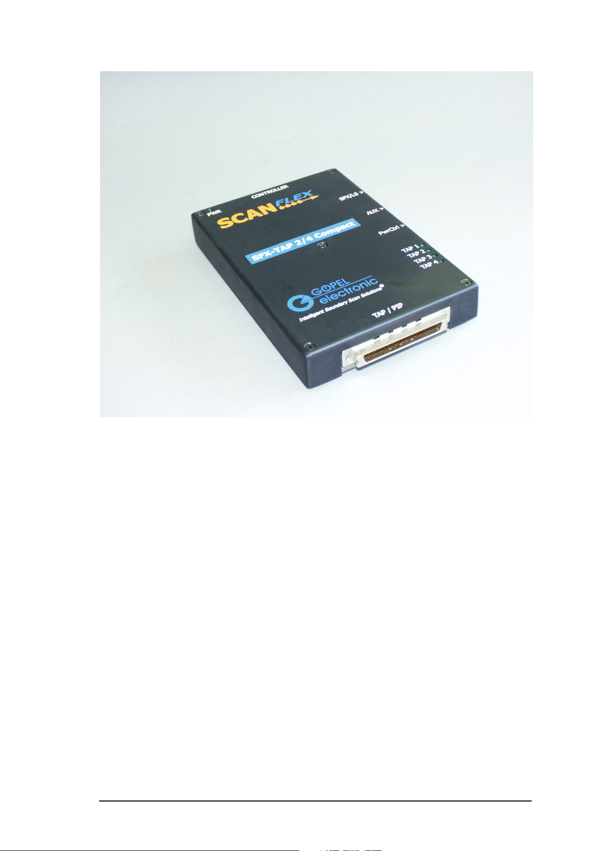
Desktop Transceiver SFX-TAP4_2/C, V0.1, Technical Description 3
Table of Contents
1
Definition ........................................................................................................................ 5
1.1
Versions of the Desktop Transceiver...................................................................... 5
1.2
Scope of Delivery.................................................................................................... 6
2
Technical Data ............................................................................................................... 6
2.1
General Information ................................................................................................ 6
2.2
Dimensions ............................................................................................................. 6
2.3
Characteristics ........................................................................................................ 6
2.4
ESD / Latch up Strength ......................................................................................... 7
2.5
Current Input ........................................................................................................... 7
3
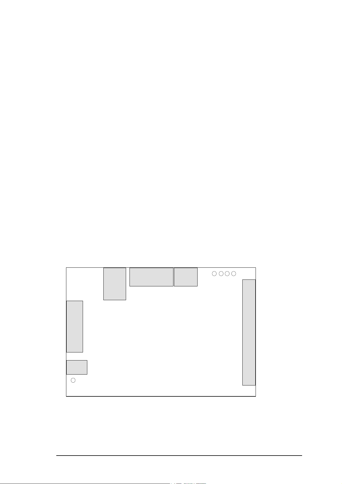
Device Structure............................................................................................................. 7
3.1
Interfaces ................................................................................................................ 7
3.2
Structure of the Desktop Transceivers SFX-TAP4/C (SFX-TAP2/C)..................... 7
3.3
AUX Connector ....................................................................................................... 8
3.4
PwrCtrl Connector .................................................................................................. 8
3.5
TAP/PIP Connector ................................................................................................ 8
4
Hardware Components .................................................................................................. 9
4.1
Voltage Supply........................................................................................................ 9
4.2
PIP Complex........................................................................................................... 9
4.3
Analog IO Signals ................................................................................................... 9
4.4
Digital IO Signals .................................................................................................... 9
4.5
Trigger Signals...................................................................................................... 10
4.6
Output Voltages .................................................................................................... 11
4.6.1
Output Voltages on TAP/PIP Connector: ...................................................... 11
4.6.2
Switch for the function of the PwrCtrl Connector:.......................................... 11
4.7
Boundary Scan Interface ...................................................................................... 12
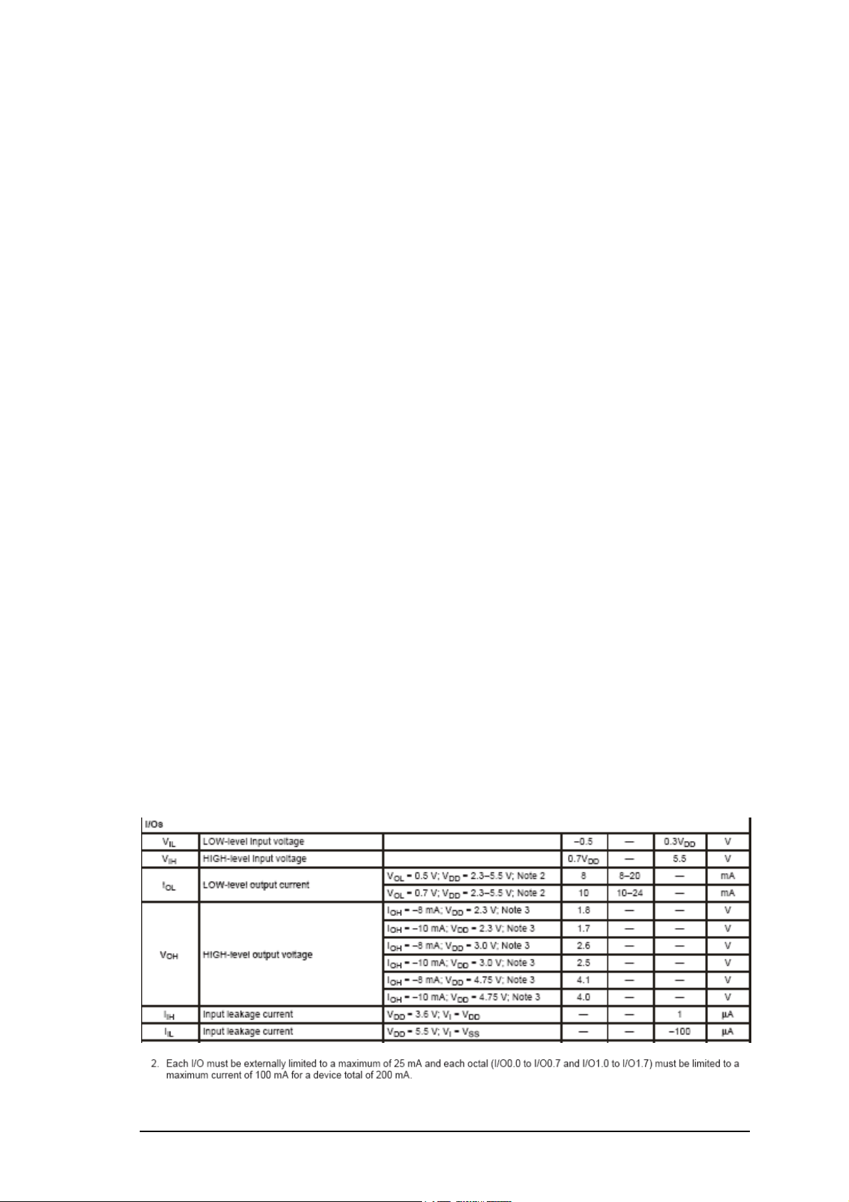
4.8
Output Driver......................................................................................................... 12
4.8.1
Absolute Maximum Ratings........................................................................... 12
4.8.2
Recommended Operating Conditions ........................................................... 13
4.8.3
Electrical Characteristics ............................................................................... 13
4.9
Input Stage............................................................................................................ 15
5
Software Settings of the Testbus Interface.................................................................. 15
5.1
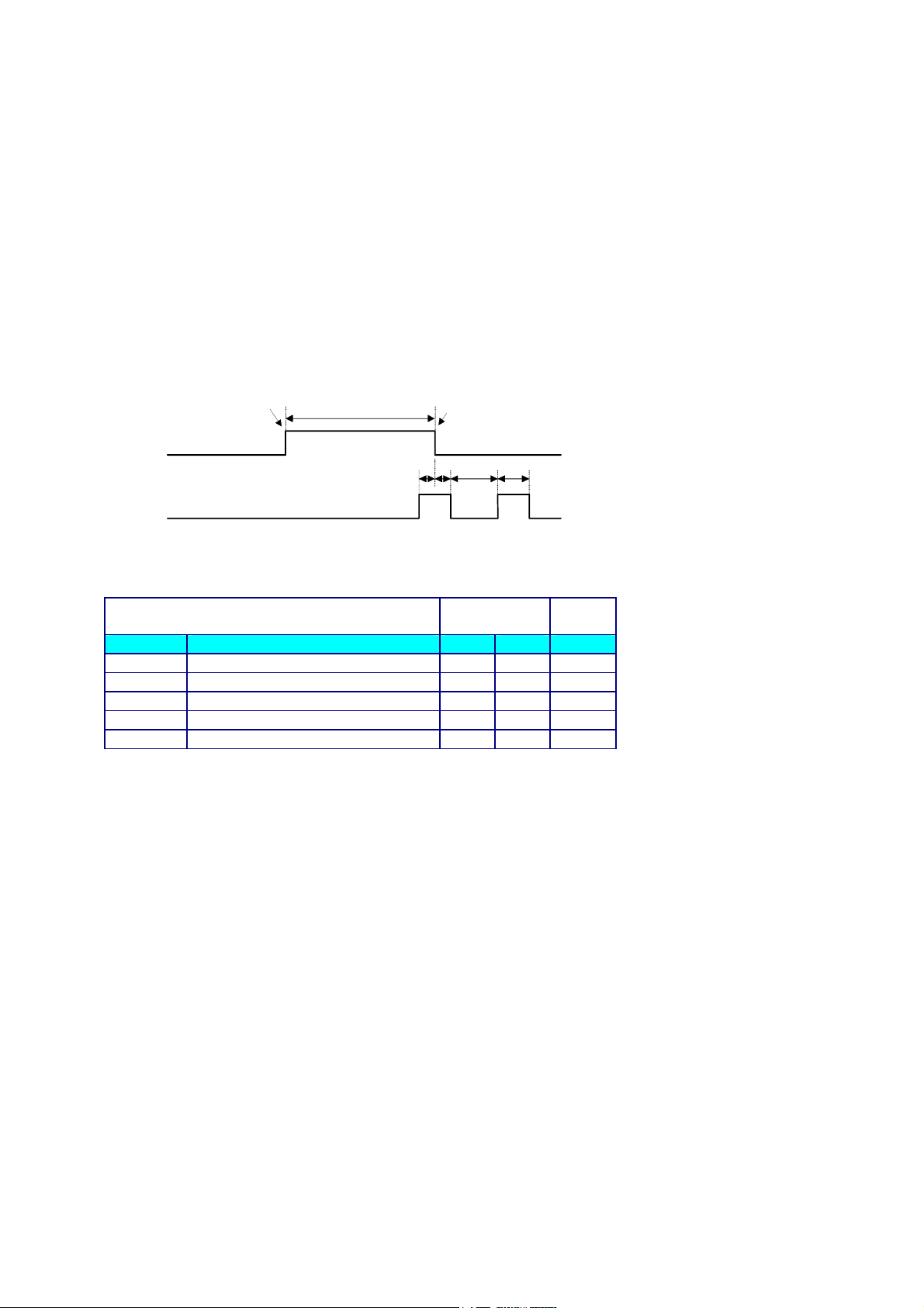
TCK Frequency..................................................................................................... 15
5.2
TAP Specific Settings ........................................................................................... 17
5.2.1
TIC Type........................................................................................................ 21
5.2.2
Output Voltage............................................................................................... 21
5.2.3
Input Voltage ................................................................................................. 21
5.2.4
Inline Resistor................................................................................................ 22
5.2.5
Pull Down Resistor ........................................................................................ 22
5.2.6
Power Relays ................................................................................................ 22
5.2.7
ADYCS II™.................................................................................................... 22
5.2.8
Testbus Signals on TAP/PIP User Interface ................................................. 25
5.2.9
SCP Controller............................................................................................... 25
6
Appendix ...................................................................................................................... 26
6.1
TAP/PIP : User Interface SFX-TAP4/C ................................................................ 26
6.2
TAP/PIP : User Interface SFX-TAP2/C ................................................................ 27
7
Order Information......................................................................................................... 28
8
References................................................................................................................... 28