Gould OS300 Service manual

www.SteamPoweredRadio.Com
I
I
I
I
I
I
I
I
I
I
I
I
I
I
I
I
I
I
I
•}
GOULf
IMPOR
T
ANT
Warranty
is
valid on/
,t
equipment with Gou/~ I you register the serial numb
f
Electronics & Electrical Prod,
Use the attached nc ers o
your
card
for
this purpose.
PRINTED 3-82
COPYRIGHT 1982
Registration Will:
l.
2.
Insure
full
protection un
Prevent
billing
for
repa1/!~;arranty
conditions.
covered by warrant
y.
Mode/ No.
0
~~
0
---
Mode/ No.
----
-----
Serial No.
---
---
OS300 20MHz
DUAL
TRACE
OSCILLOSCOPE
INSTRUCTION
MANUAL
The
information
contained herein
is
the
exclusive
property
of
Gould Inc., except
as
otherwise
indicated and shall
not
be
reproduced in whole
or
in part
without
explicit
written
authorization
from
the company. The
distribution
of
this
material outside the company may occur
only
as
authorized
by
t~e company in
writing
.
All
information
contained in this manual
is
the
latest
product
information
available at the
time
of
printing. The right
is
reserved
to
make changes
at any
time
without
not
i
ce.
Gould Inc., Instruments Division
3631
Perk
ins A
venue
.
Cl
e
vel
and
,
Oh
io
44114
1ST PRINTING
PRINTED IN U.S.A.

www.SteamPoweredRadio.Com
I
I
I
I
I
I
I
I
I
I
I
I
I
I
I
I
I
I
I
WARRANTY
AND
SERVICE
FACILITIES
Gould Oscilloscopes are warranted for a period
of
one
year from date
of
shipment
to
original purchaser.
They
are warranted
to
conform
to
the applicable published
specifications
in
effect at the time
of
shipment,
and
to
be
free from any defects
in
material
or
workmanship.
LIABILITY
OF THE
GOULD
INSTRUMENTS
DIVISION
UNDER SUCH
WARRANTY
IS
LIMITED
TO SERV-
ICING OR REPLACING
DURING
THE
WARRANTY
PERIOD
AT
THEIR
OPTION,
ANY
DEFECTIVE
PARTS
EXCE
PT
COVERS, PROBES OR FUSES
AND
DOES
NOT INCLUDE
CALIBRATION
AND
MINOR
MAIN
-
PACKING
INFORMATION
If the unit
is
to
be returned for service, it must be
adequately packed as follows:
a) Seal the unit in an oversize plastic bag.
b) Pack the bagged unit
into
a heavy
duty
cardboard
box
.
The
box
must
have a
minimum
of
2 inches
of
cushioning
on
all
six sides, so
that
the unit fits snugly.
c) Any accessories
or
instruction manuals must
be sealed into a separate plastic bag and
packed with a minimum
of
2 inches
of
cushioning between
the
instrument and
the accessories.
TENANCE
AS
OUTLINED
IN OPERATING MANUALS.
IN NO
EVENT
SHALL
THE GOULD INSTRUMENTS
DIVISION
BE
LIABLE FOR
CO
L
LATERAL
OR CON-
SEQUENTIAL
DAMAGES.
Units are
to
be returned transportation prepaid by the
buyer. The Gould Instruments Division will have the right
of
final
determination
of
the cause and existence
of
a
defect
under
this warranty. This warranty shall not
apply to
any
products
which have been subjected to
misuse, improper installation, repair, alteration, neglect,
accident,
inundation,
fire
or
operation outside their
published maximum ratings.
d) Before sealing the
box
with packing tape,
ensure
that
an official packing note
is
inserted, giving full details
of
sender's
name, address and telephone number,
instrument
type
number
and serial
number,
plus an indication
of
the reason
for
return,
and/
or
fault conditions,
if
applicable.
e) Properly label and address the outside
of
the
box
.
t)
Notify Gould
in
advance
of
shipment and ship
prepaid by United Parcel Service or equivalent.

www.SteamPoweredRadio.Com
I
I
I
I
I
I
I
I
I
I
I
I
I
I
I
I
I
I
I
ATLANTA
INSTRUMENTS DIVISION
1710
Wilwat Drive
Suite D
Norcross, Georgia
30093
Phone (404)
441-5556
BOSTON
INSTRUMENTS DIVISION
129 Middlesex
Turnpike
Burlington, Massachusetts O
1803
Phone:
(617)
272-0750
BAY AREA (CA)
INSTRUMENTS DIVISION
25936
Eden Landing Road
Hayward, CA
94545
Phone: (41 S)
887-1300
CHICAGO
INSTRUMENTS DIVISION
I001
Oakton
Street
Elk Grove Village, Illinois
60007
Phone:
(312)
640-4380
Gould
Inc
In
struments
Div
35129
Curtis
Blvd
Eastlake
Oh
44094
Phone:
(216)
361-3315
DAYTON
INSTRUMENTS DIVISION
4668
Gateway Circle
Kettering, Ohio
45440
Phone:
(St
3)
433-9586
DENVER
INSTRUMENTS DIVISION
1500
West
Hampden
Avenue
Unit
1C
Englewood, Colorado
80110
Phone
:
(303)
781-4473
DETROIT
INSTRUMENTS DIVISION
23775
Northwestern
Southfield, Michigan
48075
Phone:
(313)
355-0900
HOUSTON
INSTRUMENTS DIVISION
I
0500
Northwest Freeway
Hou ton, Texas
77092
Phone:
(713)680-1121
LA
HAM
,MD
INSTRUMENTS DIVISION
5900
Princess
Garden
Parkway
Lanham/
Seabrook
, Maryland
20706
Phone:
(301)
459-7350
SERVICE
CENTERS
LOS ANGELES
INSTRUMENTS DIVISION
2525
Campus Drive
Irvine, California 9271 S
Phone: (213} 639-7301
ORLANDO
INSTRUMENTS DIVISION
772
Northlake
Avenue
Altamonte
Springs, Florida 32701
Phone
(305)
830-0695
PHILADELPHIA
INSTRUMENTS DIVISION
GSB Building
Belmont & City Line Avenue
Bala
Cynwyd,
Pennsylvania 19004
Phone
:
(215)
839-7066
PITTSBURGH
INSTRUMENTS DIVISION
Campbells
Run
Road
Parkway West
Pittsburgh, Pennsylvania 15205
Phone
:
(412)
923-2160
SADDLEBROOK
INSTRUMENTS DIVISION
74 Kenney Place
Saddle
Brook,
New Jersey
07662
Phone
:
(201)
845-0220
SEATTLE
INSTRUMENTS DIVISION
The
Commons
Bldg. Suite C-155
I
200
I
12th
Avenue NE
Bellevue, Washington
98004
Phone:
(206)
453-8100
TORONTO
ALLAN CRAWFORD ASSOC., LTD
6503
Northam
Drive
Mississauga,
Ontario
, Canada
Phone:
678-1500
EUROPE
GOULD INSTRUMENTS S.A.F.
57 rue St. Sauveur
91160
Ballainvilliers,
France
Phone: 909-10-67
GOULD INSTRUMENTS DIVISION
Roebuck Road
Hainault, E sex, England
Phone
:
01
-
500
-
1000
GOULD INSTRUMENTS DIVISION
Dieselstrasse
5-
7
D-64S3 Seligenstad
t,
West Germany
Phone:
06182-3107

www.SteamPoweredRadio.Com
I
I
I
I
I
I
I
I
I
I
I
I
I
I
I
I
I
I
I
Contents
SECTION
1
Introduction
SECTION
2
Specification
SECTION
3 Operation
3.1
Connection
to
the supply
3.2 Obtaini
ng
a Trace
3.3 Setti
ng
up the Y channels
3.4 Display Modes
3.5 Timebase and X Expansion
3.6 Trigger
3.7
Additional
Facilities
SECTION
4
Circuit Description
4.1 General
4.2 The Y
Amplifier
and Beam Switch
4.3 The Trigger Circui
ts
4.4 The Timebase Generator and
X
amplifier
4.5 The Mode
Control
Circuits and
Calibrator
4.6 The Power Supplies and C.R.T.
Circuits
1.1
2.1
3.1
3.1
3.1
3.1
3.2
3.2
3.2
3.3
4.2
4.2
4.2
4.3
4.3
4.4
4.5
SECTION
5
Maintenance
5.2
5.1
General 5.2
5.2 Access 5.2
5.3 Fault Findi
ng
5.3
5.4 Setti
ng
-
up
Procedure 5.5
SECTION
6
Component
Lists
and
Circuit
Diagrams
6.1
SECTION
7 Guarantee
and
Service Facilities
7.1
ILLUSTRATIONS
Fig.
1 Block Diagram 4.1
Fig
. 2
Internal Assembly -
top
view 5.1
Fig.
3
Internal Assembly -
bottom
view 5.3
Fig.
4
Circuit
Diagram, Y
Ampl
ifi
er
6.8
Fig
.
5 Circuit Diagram, Ti
mebase
&
Tr
i
gger
6.9
Fig.
6 Ci
rcuit
Diagram, Power Supply
and C.R.T. Circuits 6.
10
Fig.
7
Mechanical Views
6.11

www.SteamPoweredRadio.Com
I
I
I
I
I
I
I
I
I
I
I
I
I
I
I
I
I
I
I
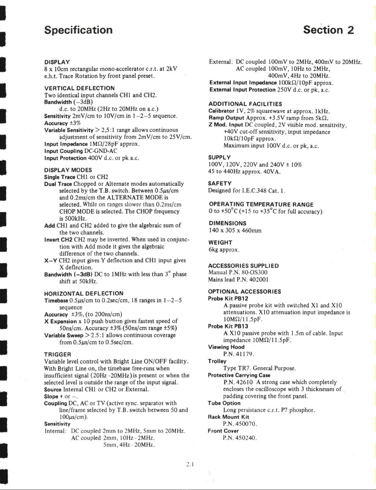
Introduction
The OS300
is
a versatile general purpose dual trace
oscilloscope intended for general laboratory, industrial,
servicing and educational applications. The full 8 x 10cm
rectangular tube provides a bright display against the
calibration graticule.
It features two identical input channels with a maximum
sensitivity
of2mV
/cm and a bandwidth from D.C.
to
20MHz. These channels may be displayed separately or
together in dual trace mode. Alternatively they can be
added
or
subtracted for sum
or
difference display. The
timebase ranges from 0.2s/cm
to
O.Sµs/cm
and
ax
10
expansion facility extends this to S0ns/cm. Independent
variable sensitivity and sweep rate controls are provided.
I.
I
Section 1
Particular
attention
has been paid
to
trigger performance,
with D.C. and A.C. coupling available and a bright-line
free-run facility
to
enable trace location in the absence
of
trigger. An active T.V. synch separator
is
provided for
those working with video waveforms.
The OS300 includes many facilities such
as
a IkHz
calibrator, a D.C. coupled Z modulation input and a
trace rotation control, usually found only on the more
expensive instruments.
This compact instrument
is
readily portable. The
internal construction
is
based largely on a single printed
circuit board assembly
to
provide easy access for main-
tenance and minimum cost
of
ownership.

www.SteamPoweredRadio.Com
I
I
I
I
I
I
I
I
I
I
I
I
I
I
I
I
I
I
I
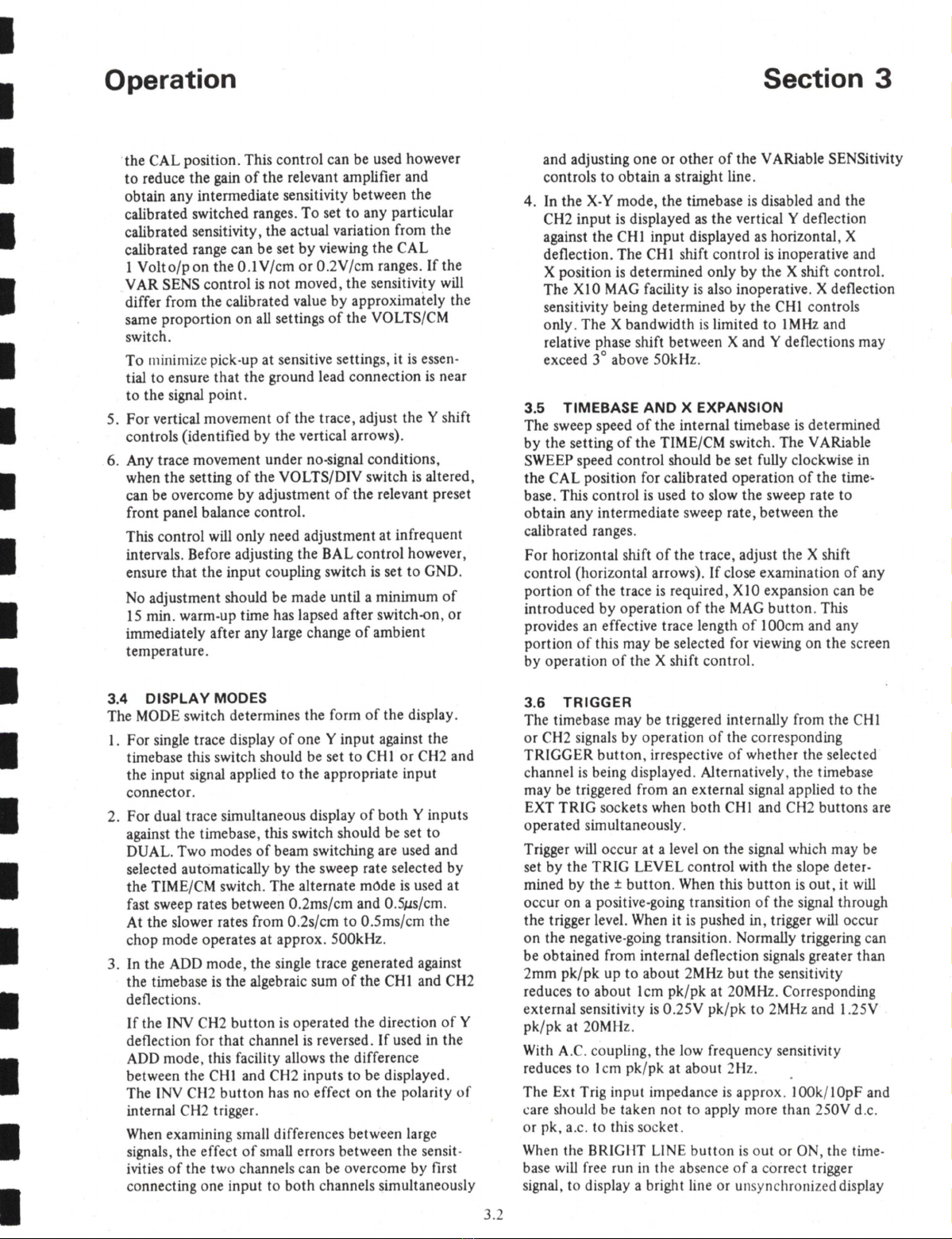
Specification
DISPLAY
8 x 10cm rectangular mono-accelerator c.r.t. at 2kV
e.h.t. Trace Rotation
by
front panel preset.
VERTICAL
DEFLECTION
Two identical input channels CHI and CH2.
Bandwidth (-3dB)
d.c.
to
20MHz (2Hz
to
20MHz on a.c.)
Sensitivity 2mV/cm
to
lOV/cm
in
1- 2- 5 sequence.
Accuracy
±3
%
Variable Sensitivity >2
,5
:I range allows continuous
adjustment
of
sensitivity from 2mV/cm
to
25V/cm.
Input Impedance IM!1/28pF approx.
Input Coupling DC-GND-AC
Input Protection 400V d.c. or pk a.c.
DISPLAY
MODES
Single
Trace CHI
or
CH2
Dual Trace Chopped
or
Alternate modes automatically
selected
by
the T.B. switch. Between 0.5µs/cm
and 0.2ms/cm the ALTERNATE MODE
is
selected. While
on
ranges slower than 0.2ms/cm
CHOP MODE
is
selected. The CHOP frequency
is
S00kHz.
Add CHI and CH2 added
to
give the algebraic sum
of
the two channels.
Invert CH2 CH2 may be inverted. When used in conjunc-
tion with Add mode it gives the algebraic
difference
of
the two channels.
X-Y
CH2 input gives Y deflection and CHI input
gives
X deflection.
Bandwidth
(-3dB)
DC
to 1MHz with less
than
3° phase
shift at 50kHz.
HORIZONTAL
DEFLECTION
Timebase 0.5µs/cm
to
0.2sec/cm, 18 ranges in 1- 2- 5
sequence
Accuracy
±3
%,
(to
200ns/cm)
X Expansion x 10 push
button
gives fastest speed
of
50ns/cm. Accuracy ±3% (S0ns/cm range ±5%)
Variable
Sweep
>2
.5
:1 allows continuous coverage
from 0.5µs/cm
to
0.5sec/cm.
TRIGGER
Variable level control with Bright Line
ON/OFF
facility.
With Bright Line
on,
the timebase free-runs when
insufficient signal (20Hz -20MHz)
is
present or when the
selected level
is
outside the range
of
the input signal.
Source
Internal CHI
or
CH2 or External.
Slope+ or
-.
Coupling
DC
,
AC
or TV (active sync. separator with
line/frame selected by T.
B.
switch between 50 and
I0Oµs/cm).
Sensitivity
Internal: DC coupled 2mm to 2MHz, 5mm
to
20MHz.
AC
coupled 2mm,
IOH
z- 2
MH
z.
5mm , 4Hz- 20MHz.
2.
1
Section 2
External:
DC
coupled IO0mV
to
2MHz, 400mV
to
20MHz.
AC
coupled IO0mV, IOHz
to
2MHz,
400mV, 4Hz
to
20MHz.
External Input Impedance 100k!1/10pF approx.
External Input Protection 250V d.c. or pk, a.
c.
ADDITIONAL
FACILITIES
Calibrator
IV
,
2%
squarewave at approx. IkHz.
Ramp Output Approx.
+3
.5V ramp from 5k!1.
Z Mod. Input
DC
coupled, 2V visible mod. sensitivity,
+40V cut-offsensitivity, input impedance
10k!1/10pF approx.
Maximum input lO0V d.c.
or
pk, a.c.
SUPPLY
I00V, 120V, 220V and 240V ± I
0%
45
to
440Hz approx. 40VA.
SAFETY
Designed for I.E.C.348 Cat. 1.
OPERATING
TEMPERATURE
RANGE
0
to
+50°C (+15
to
+35°C for full accuracy)
DIMENSIONS
140 X 305 X 460mm
WEIGHT
6kg approx.
ACCESSORIES SUPPLIED
Manual P.N. 80-OS3
00
Mains lead P.N. 402001
OPTIONAL
ACCESSORIES
Probe
Kit
PB12
A passive probe kit with switched XI and
XI0
attenuations.
XI
0 attenuation input impedance
is
l0M!1/11.5pF.
Probe
Kit PB13
A
XI0
passive probe with 1.5m
of
cable. Input
impedance IOM!1/l l .5pF.
Viewing Hood
P.N.41179.
Trolley
Type
TR
?.
General Purpose.
Protective Carrying
Case
P.
N.
42610
Astrong case which completely
encloses the oscilloscope with 3 thicknesses
of
padding covering the front panel.
Tube Option
Long pe
rsi
stance c.r.t.
P7
phosphor.
Rack Mount Kit
P.N.
4500
7
0.
Front Cover
P.N. 4502
40
.

www.SteamPoweredRadio.Com
I
I
I
I
I
I
I
I
I
I
I
I
I
I
I
I
I
I
I
Operation
INTERNATIONAL
SAFETY
WARNING
(as
required
for
1.E.C.
348
Class
I)
This instruction manual contains
information
and
warnings which must be observed
by
the user
to
ensure
safe
operation
and retain
the
apparatus
in
a safe
condition.
The
instrument
has been designed for
indoor
use within
the
specified limits
of
temperature.
It should
not
be switched
on
if
there are obvious signs
of
mechanical damage and it should
not
be used
under
wet
conditions.
GROUNDING
The instrument must be
operated
with
a protectiveground
connected
via
the
appropriate (yellow/green)
conductor
of
the
supply cable. This
is
connected
to
the
instrument
before
the
line and neutral supply
connectio
ns when
the
supply socket
is
inserted
into
the plug
on
the
back
of
the
instrument.
If
the
final
connection
between
the
instru-
ment
and the supply is made elsewhere,
the
user must
ensure
that
the
ground
connection
is
made before line
and neutral.
If
any
supply cable
other
than
that
supplied with
the
instrument
is
used, it must carry an adequate protective
ground
conductor.
Any
interruption
of
the protective
earth
conductor
inside
or
outside the
instrument
is
likely
to
make
the
instrument dangerous.
Intenti
onal
interruption
is
prohibited.
Signal connections
into
the
instrument
should
be
connected
after
and disconnected before
the
protective
ground
connection
is
made, i.e. the supply lead must be
connected at all times that signal leads are
connected.
LIVE
PARTS
The
instrument
is
safe
to
operate
with
the
covers fitted
and these must
not
be removed
under
normal usage. The
covers
protect
the user from live parts and
they
should
be removed only
by
suitably qualified personnel for
maintenance
or
repair purposes. (see maintenance
section).
VENTILATION
The
OS300 relies
on
convection cooling and must
not
be
operated in a position which restricts the external circu-
lation
of
air.
3.1 CONNECTION TO
THE
SUPPLY
I . Before connecting the OS300
to
the
supply, check
that the supply range switches are set
to
suit the
supply voltage to be used and that the correct fuse
is
fitted . Note that the fuse has
to
be changed when
switching between the I
00V
and
220V
ranges.
The
switches and fuse holder are
mounted
on
the
ba<.:k
panel
of
the
instrument.
Do
not
operate
the range
selection switches while the
OS300
is
switched on.
3.1
Section 3
3.2
OBTAINING
A TRACE
I. After
connection
to
the
supply, switch
on
by turning
the INTENSITY
control
clockwise away from the
OFF
position. Check
that
the
POWER indicator
L.E.D. lights.
2. Set
the
:
MODE switch
to
CHI
CHI Y shift
control
(vert. arrows)
to
approx. mid
setting.
CHI
VAR
SENS control fully clockwise
to
the
C
AL
position.
CHI
input
coupling switch
to
GND.
BRIGHT LINE
button
out
(ON)
.
X
MAG.
button
out
(XI)
X
shift
control
(horiz. arrows)
to
approx
. mid
setting.
TIME/CM switch
to
5µs.
A horizontal trace should appear
on
the screen
as
the
INTENSITY
control
is
advanced.
3. Adjust
the
INTENSITY
control
to
obtain
a display
of
the
required brightness.
4.
Adjust
the
FOCUS
control
to
obtain
a sharply
defined trace.
5.
Adjust the CH
I
Y shift
control
and the
X
shift
control
tocentralize the trace
on
the
screen.
6. Adjust
the
TRACE
ROTATE preset
control
if
neces-
sary
to
align
the
trace
with
the
center
graticule line.
It
may be necessary
to
re-adjust this
control
only
when
the
instrument
is
re-positioned
as
the beam
deflection can be affected
by
earths magnetic field or
other
sources
of
magnetic radiation.
NOTE:
The
OS300
should
not
be
operated
close
to
sources
of
alternating magnetic field such
as
large
transformers as these
may
interfere
with
the trace.
3.3 SETTING
UP
THE Y CHANNELS
I . Using a coaxial
input
signal lead,
connect
a signal
to
the
CHI
or
CH2
input
socket,
2.
For
(a)Direct
connection
of
the
input
signal, set the
associated AC-Ground-DC slide switch
to
DC.
(b)
Capacitive coupling
of
the
input
signal through
an internal 0 .
lµF
400V
capacitor, set
the
slide
switch
to
AC
.
NOTE: When examining low amplitude a.c. signals
superimposed
on
a high d.c. level, the slide
switch should
be
set
to
AC and the sensitivity
of
the
Y
amplifier increased
as
in
(4).
3.
To
locate the base line, set the slide switch
to
the
c;
D s
etting
.
At
this setting, the
input
signal
is
open
<.:ir<.:uit
and the input
to
the amplifier
is
connected
to
ground.
4.
To
select sensitivity, set the VOLTS/
CM
switch
to
the
required range.
For
calibrated
operation,
the
VARiable
SENSitivity
control
should be set fully clockwise
to

www.SteamPoweredRadio.Com
I
I
I
I
I
I
I
I
I
I
I
I
I
I
I
I
I
I
I
Operation
the CAL position. This control can be used however
to
reduce the gain
of
the relevant amplifier and
obtain any intermediate sensitivity between the
calibrated switched ranges. To set
to
any particular
calibrated sensitivity, the actual variation from the
calibrated range can be set
by
viewing the CAL
I
Volto/pon
the0.IV/cm
or0
.2
V/cm ranges.
If
the
VAR SENS control
is
not moved, the sensitivity will
differ from the calibrated value by approximately the
same proportion on all settings
of
the VOLTS/CM
switch.
To minimi
ze
pick-up at sensitive settings, it
is
essen-
tial
to
ensure that the ground lead connection
is
near
to
the signal point.
5. For vertical movement
of
the trace, adjust the Y shift
controls (identified by the vertical arrows).
6. Any trace movement under no-signal conditions,
when the setting
of
the VOLTS/DIV switch
is
altered,
can be overcome by adjustment
of
the relevant preset
front panel balance control.
This control will only need adjustment at infrequent
intervals. Before adjusting the BAL control however,
ensure that the input coupling switch
is
set
to
GND.
No adjustment should be made until a minimum
of
15
min. warm-up time has lapsed after switch-on, or
immediately after any large change
of
ambient
temperature.
3.4 DISPLAY MODES
The MODE switch determines the form
of
the display.
I.
For single trace display
of
one Y input against the
timebase this switch should be set
to
CHI or CH2 and
the input signal applied to the appropriate input
connector.
2. For dual trace simultaneous display
of
both
Y inputs
against the timebase, this switch should be set
to
DUAL. Two modes
of
beam switching are used and
selected automatically by the sweep rate selected by
the TIME/CM switch. The alternate mode
is
used at
fast sweep rates between 0.2ms/cm and 0.5µs/cm.
At the slower rates from 0.2s/cm
to
0.5ms/cm the
chop mode operates at approx. 500kHz.
3. In the ADD mode, the single trace generated against
the timebase
is
the algebraic sum
of
the CHI and CH2
deflections.
If
the INV CH2
button
is
operated the direction
of
Y
deflection for that channel
is
reversed .
If
used in the
ADD mode, this facility allows the difference
between the CHI and CH2 inputs to be displayed.
The
INV
CH2
button
has no effect on the polarity
of
internal CH2 trigger.
When
examining small differences between large
signals, the effect
of
small errors between the sensit-
ivities
of
the two channels can be overcome by first
connecting one input to
both
channels simultaneously
3
.2
Section 3
and adjusting one
or
other
of
the VARiable SENSitivity
controls
to
obtain a straight line.
4. In the
X-Y
mode, the timebase
is
disabled and the
CH2 input
is
displayed
as
the vertical Y deflection
against the CHI input displayed
as
horizontal, X
deflection. The CHI shift control
is
inoperative and
X position
is
determined only by the X shift control.
The XI 0
MAG
facility
is
also inoperative. X deflection
sensitivity being determined by the CHl controls
only. The X bandwidth
is
limited to
1MHz
and
relative phase shift between X and Y deflections may
exceed 3° above 50kHz.
3.5 TIMEBASE AND X EXPANSION
The sweep speed
of
the internal timebase
is
determined
by
the setting
of
the TIME/CM switch. The VARiable
SWEEP speed control should be set fully clockwise in
the CAL position for calibrated operation
of
the time•
base. This control
is
used
to
slow the sweep rate to
obtain any intermediate sweep rate, between the
calibrated ranges.
For horizontal shift
of
the trace, adjust the X shift
control (horizontal arrows). If close examination
of
any
portion
of
the trace
is
required,
Xl0
expansion can be
introduced by operation
of
the
MAG
button
. This
provides
an
effective trace length
of
l00cm and any
portion
of
this may be selected for viewing on the screen
by operation
of
the X shift control.
3.6 TRIGGER
The timebase may be triggered internally from the CHl
or
CH2 signals by operation
of
the corresponding
TRIGGER
button,
irrespective
of
whether the selected
channel
is
being displayed. Alternatively, the timebase
may be triggered from an external signal applied to the
EXT TRIG sockets when both CHl and CH2 buttons are
operated simultaneously.
Trigger
will
occur at a level on the signal which may be
set by the TRIG LEVEL control with the slope deter-
mined by the ±
button
. When this
button
is
out,
it will
occur
on
a positive-going transition
of
the signal through
the trigger level. When it
is
pushed in, trigger will occur
on
the negative-going transition. Normally triggering can
be obtained from internal deflection signals greater than
2mm
pk/pk
up to about 2MHz but the sensitivity
reduces to about 1cm
pk/pk
at 20MHz. Corresponding
external sensitivity
is
0.25V
pk/pk
to 2MHz and 1.25V
pk/pk
at 20MHz.
With A.C. coupling, the low frequency sensitivity
reduces to Icm
pk/pk
at about 2Hz.
The Ext Trig input impedance
is
approx. I00k/1
0pF
and
c.:are
should be taken not to apply more than 250V d.c.
or pk, a.c. to this socket.
When the BRIGI
IT
LINE
button
is
out or O , the time-
base will free run
in
the absence
of
a correct trigger
sig
nal, to display a bright line or
un
synchronizeddisplay

www.SteamPoweredRadio.Com
I
I
I
I
I
I
I
I
I
I
I
I
I
I
I
I
I
I
I
Operation
until the level control
is
adjusted
and/or
the amplitude
of
the trigger signal
is
increased. This free-run action in
the absence
of
correct trigger, helps in finding the trace
and leads
to
ease
of
operation.
If
the timebase
is
required
to
free-run continuously, the LEVEL control
should be set to either end
of
its rotation.
It
is
expected
that
the BRIGHT-LINE
OFF
mode will
be selected only when the instrument
is
to be used to
display signals
at
repetition rates less than 40Hz
or
faster
than 2MHz. This will prevent additional free run sweeps
from occurring between correctly triggered low
frequency sweeps or erratic high frequency operation.
The coupling
of
the trigger signal may be selected as a.c.
or
d.c. by operation
of
the corresponding
TRIGGER
button
. When
both
are pressed, an active synch.
separator circuit
is
introduced
to
provide line
or
frame
triggering for video waveforms. Field trigger occurs at
low sweep rates up
to
IOOµs/cm
and line trigger
is
auto-
matically selected on fast sweep rates from SOµs/cm.
The trigger polarity should be selected for
the
polarity
of
the synch. pulses. At least
2mm
pk/pk
of
synch. pulse
amplitude
is
required with internal triggering
or
0.25V
with external.
Summarizing the use
of
the
trigger controls for most
applications:
a) With BRIGHT LINE ON
(button
out)
, select the
trigger source
CH
I, CH2
or
EXT and the coupling
required, a.c.
or
d.c.
b) Select the trigger slope +
or
-and adjust the trigger
level control
to
obtain a stable trace, starting at the
required point
on
the waveform.
3.7
ADDITIONAL
FACILITIES
l . Calibrator
This
output
pin on the front panel provides a positive
going 1V flat topped square wave at approx. IkHz.
It
can be used to check the sensitivity
of
the instru-
ment
or
to set
to
any particular calibrated sensitivity
(see section 3.3.4). The rise time
is
approx.
2µs
and
the
output
impedance
is
approx.
470il,
providing
approx. 2.3mA when shorted
to
ground.
The CAL
output
may be used also to set up passive
probes (see section 3.7.
4)
.
2. Ramp
Output
This
4mm
socket
on
the
rear panel provides a d.c.
coupled positive-going ramp generated
by
the
J.J
Section 3
timebase
of
approx. +3.SV pk from an impedance
of
approx. Sk ohms.
If
a lower
output
level can be
tolerated, distortion
of
fast ramp
output
signals due
to
capacitive loading can be avoided
by
adding resis-
tive loading
to
attenuate
the signal.
3. Z mod
This socket
on
the rear panel allows modulation
of
the brightness. The input
is
d.c. coupled into approx.
I
Okil/
lOpF. The sensitivity at normal brightness
settings requires about 2V
to
provide visible
modulation. Approx. +40V
is
required to provide full
trace blanking.
Care should be taken
not
to apply more than I
OOV
d.c.
or
pk, a.c. to this socket.
4.
Use
of
the
Passive Probe
A XI Opassive probe may be used
to
extend the
voltage range and increase the
input
impedance
of
the
Y amplifiers. The
input
resistance
of
a Y channel
is
I
OM
ohms, shunted
by
approximately
28pF
. The
effective capacitance
of
the
input lead must be added
to
this and the resultant impedance can
often
load
the signal source. Therefore it
is
advisable
to
use a
IM ohms, XlO probe such
as
PB12
or
PB13. This
reduces the input capacitance and increases the input
resistance, at the expense
of
a 1
OX
reduction in
sensitivity. The probe inserts a shunt
RC
network in
series
to
form a 10:I
attenuator
with
the
input
RC
of
the Y channel.
To
obtain a flat frequency response
it
is
necessary to adjust the capacitance
of
the probe
to match the input capacitance
of
the Y channel
as follows:
I. Set the Y channel VOLTS/CM switch
to
20mV,
the TIME/CM switch to
SOOµs
and trigger from
the appropriate channel.
2. Connect the probe to the CAL socket.
3. Adjust the probe compensation
to
obtain a level
trace, i.e. flat
top
without overshoot
or
under-
shoot.
5. Camera
A camera may be used with the oscilloscope
to
record
waveforms. This facility
is
particularly useful at slow
timebase sweep rates. Suitable cameras utili
zi
ng
Polaroid film may be obtained from Shackman and
hand held against the tube face. Other oscilloscope
cameras may be used
but
suitable adaptors must be
obtained and should be discussed with the camera
manufacturer.

www.SteamPoweredRadio.Com
~
~~~~---------------
"'ti
~-
CX)
g
~
c:,
~-
ii::
3
CHl
(X)
1/P
CH2
(Y)
1/P
EXT
TRIG
1/P
~
ATTENUATOR
~
ATTENUATOR
-
PRE
-
AMPLIFIER
PRE
,
AMPLIFIER
-
-
-->
-
,.
TRIGGER
-
AWLIFIER
-
BEAM
::
Y
OUTPUT
SW
I
TCH
AMPLIF
I
ER
-
BEAM
CHOP
SWITCH
-
MULTIVIBRATOR
BISTABLE
MONOSTABLE
::
TV
SYNC
HOLD
OFF
SEPARATOR
::
1•
::
SCHMITT
TRIGGER
CRT
-\ I
,
0-
7
-
,IX
J--
-
BLANKING
---
--
AMP
•
~
~
::
RAMP
TB_
C
XY
GENERATOR
' '
·~
-
TIMEBASE
-
-X
SET
BI
STAB
LE
RESET
AMPLIF
I
ER
("')
-·
~
n
C
;::.·
C
ff)
CA
n
~
-·
"'C
r+
-·
0
::::,
"'
ff)
n
r+
-·
0
::::,
~

www.SteamPoweredRadio.Com
I
I
I
I
I
I
I
I
I
I
I
I
I
I
I
I
I
I
I
Circuit Description
To aid
component
location, circuit references have been
allocated in the following general pattern.
99 Components
not
mounted
on
printed
circuit boards.
100 199 Components
mounted
on
the
attenuator
assemblies.
200
299 Pre-amplifier and Ramp Generator
components
mounted
on the daughter
board.
300 -399 Y Pre-amplifier and Beam Switch
components
mounted
on
the main board.
400 -499 Y Amplifier and Y
Output
Amplifier
components mounted on the main board.
500 599 Timebase and X
Output
Amplifier
components mounted
on
the main board.
600 699 Trigger circuit
components
mounted on
the main board.
700 799 Power supply and Modulation Circuit
components on the main board.
4.1
GENERAL
Referring
to
the
block diagram (Fig.
I)
signals applied
to
the CHI and CH2 input sockets pass into their respective
attenuators and amplifiers. The VOLTS/CM switch
controls the gain
of
the pre-amplifier in steps
of
1.2.5
sequence to cover the ranges from 2mV/cm
to
0.1 V/cm
and a + I
00
attenuator
is
introduced before the
amplifier
on
the ranges 0
.2
V/cm to IOV/cm.
The Variable Gain control adjusts the amplifier gain to
give
I to 2
.5
times reduction
of
gain on all settings
of
the Volts/cm switch. The fast electronic beam switch
selects either the CHI
or
the CH2 signal to be amplified
further and passed
to
the Y deflection plates
of
the c.r.t.
A sample
of
each signal
is
taken and passed
to
the trigger
switch bank where selection
of
CH
I,
CH2 or Ext trig
source
is
made.
The selected signal
is
amplified and passed to the
Schmitt trigger, the
output
of
which clocks the timebase
bistable "
on"
. The ramp generator then begins to
generate its linear ramp, which, after passing through the
X amplifier,
is
applied to the X deflection plates
of
the
c.r.t. and drives the electron beam linearly across the
tube face. A portion
of
the signal from the ramp
generator
is
fed back
to
the hold-off circuit, shutting the
gate
to
prevent any further pulses from the Schmitt
trigger from reaching the timebase bistable during the
ramp period. When the ramp has reached the necessary
maximum level, the timebase bistable
is
reset, and the
ramp
is
quickly returned to its quiescent state. A time-
constant in
the
hold-off circuit retains this signal
to
inhibit another ramp from being initiated for a short
period, until the ramp timing capacitor
is
discharged
fully . Thus a ramp
is
generated at a rate set by the
TIME/CM switch when the trigger signal reaches a pre-
determined level. This ramp sweeps the beam across the
4
.2
Section 4
c.r.t. face , returns and waits for the next input cycle to
reach the set trigger point, so producing subsequent
ramps. The timebase bistable
is
connected
to
a blanking
amplifier whose function
is
to
turn
on
the electron beam
during the sweep and blank it
off
during the fly-back
and subsequent waiting period.
At fast sweep rates for a dual trace display, the
TIME/CM switch automatically selects the alternate
sweep mode
of
control for the beam switch. At the end
of
each sweep, the signal from the timebase reverses the
state
of
the
beam switch bistable, causing alternate
displays
of
the
CH
I and CH2 signal
on
successive sweeps
of
the timebase. At slow sweep rates,
the
chop mode
is
selected, when the
chop
multivibrator free runs indepen-
dently, causing the beam
to
switch on chop between
CHI and CH2 levels during the sweep.
A signal from the multivibrator also blanks the trace
during each switching transitition. With CHI
or
CH2
only selected,
the
beam switch bistable
is
held
to
select
that channel only.
In
the
X-Y
mode, the bistable
is
held
to select CH2 as the Y deflection signal, while an
additional switch diverts the
output
from the
CH
I pre-
amplifier, to
the
X
output
amplifier
as
the X deflection
signal in place
of
the
normal ramp signal. The blanking
amplifier
is
held
in
the bright-up state. When TV trigger
mode
is
selected, an additional synch. separator circuit
is
introduced into the signal path leading into the trigger
amplifier.
4.2
THEY
AMPLIFIERS
AND
BEAM SWITCH
These circuits are shown
in
Fig. 4.
The attenuators and pre-amplifiers
of
channel I are
identical
to
those
of
channel 2 and accordingly only
channel I
is
described.
The input signal
is
applied to SKA and then
to
the
attenuator
via
the
3 position slide switch, SIOI. This
allows the input signal
to
be directly coupled through in
the
DC
position or coupled via C105 in the
AC
position.
In
the central GND position, the input signal from
SKA
is
left open circuited while the input
to
the
attenuator
is
grounded.
On the most sensitive ranges, 2mV/cm to IOOmV/cm,
the VOLTS/CM switch, S102, couples the signal through
directly
to
the pre-amplifier and the network resistor,
RNIO!c,
provides the input impedance. On the
remaining ranges, SI
02
introduces RI
01
a into the signal
path to form a 100:I
attenuator
with RN!Ol
bin
parallel with
RNI0lc
.
High frequency compensation
of
the
attenuator
is
pro-
vided
by
CIOI and
CI04
while
Cl02
with C106 allows
the input capacitance
of
the
attenuator
to be set
to
equalise that
of
the unattenuated ranges.
Diodes, D201 and D202 with R
207,
provide input
protection by limiting the input voltage appled to the
amplifier
to
the voltages
of
zencr diode, D203 and the
positive supply line.

www.SteamPoweredRadio.Com
I
I
I
I
I
I
I
I
I
I
I
I
I
I
I
I
I
I
I
Circuit Description
The input stage
of
the pre-amplifier
is
formed
by
the
f.e.t. source followers, TR201 and
TR202,
and
emitter
followers,
TR204
and
TR203.
Unbalance in this stage
is
corrected
by
the BAL control
potentiometer,
R301 .
The input stage drives the divider
network
, RN201 . The
VOLTS/CM switch second wafer, S201, selects the
necessary
output
, either directly via RN201 on the 2mV
or
200mV
ranges,
or
attenuated
by
2.5,
5, 10, 25
or
50
times
on
the subsequent ranges. This network presents a
constant
output
impedance and further
attenuation
is
introduced
by
the
shunt action
of
the VARIABLE
sensitivity control, R217. The resultant signal
is
amplified by the integrated amplifier, IC301 . The ampli-
fier gain
is
determined by R309 and the preset, R302.
The differential
output
is
balanced
by
the bias through
R308 from the preset, R307.
The differential
output
from IC301
(CHI)
or
from
IC35 l (CH2)
is
selected
by
the beam switch
as
the
input
for the subsequent shunt feedback amplifier stage
formed
by
TR401,
TR402
. The signal input currents are
defined by R3 l6 and R3 l7 and are summed with the Y
shift currents defined by
R3
l8 and
R3
l9 from the
CH
I
shift control, R3 I5. The corresponding
components
for
channel 2 are R366, R367, R368, R369 and R
365.
Channel 2 only differs for channel I
by
the addition
of
the double pole changeover switch, S301, which reverses
the
output
signals from IC351 in the INVERT mode.
The beam switch
is
formed by the 8 diode gate, D301,
D302,D303
,
D304,D351,D352
,D353,D354.The
relative control potentials from IC501 allow either the
signal current from IC301
and/or
IC351
to
reach the
bases
ofTR401
and
TR402
, or divert those currents
from the bases.
The
outputs
from the differential shunt feedback ampli-
fier stage formed by TR401 and
TR402,
are fed
to
the
gounded emitter amplifier stage,
TR403
and
TR404
.
This in turn feeds the differential cascode Y ou
tput
stage
TR405,
TR406,
TR407
and
TR408
to drive the Y
deflection plates
of
the c.r.t.
High frequency compensation
of
the
output
amplifier
is
provided by networks between the emitters
of
TR403
and
TR404
and those
of
TR405
and
TR406.
Adjust-
ment
of
this compensation is
by
C402 and C405.
4.3 THE
TRIGGER
CIRCUITS
These circuits are shown in Fig. 5.
The Trigger Source switches, S502 and S503, connect
the required trigger signal via the Trigger Coupling
switches, S504 and S505, to
the
trigger buffer amplifier
formed
by
TR601 and
TR602
. S502 selects the differen-
tial CHI signal
via
R313 and R314
frow.
IC301 (Fig.
4)
.
S503 selects the equivalent CH2 signal via R363 and
R364 from IC35
l.
Where
both
S502 and S503 are
selected,
both
of
the above signals are disconnected and
the single-sided
input
from the EXT TRIG input socket
SKC'
is
selected.
4.3
Section 4
When the
AC
coupling switch, S504,
is
out
, the trigger
signals are directly coupled-through,
but
when this
switch
is
in,
AC
coupling
is
introduced via C603 and
C604 (C60I on External). TR601 and
TR602
form a
differential buffer amplifier with the
DC
balance
controlled by the
TRIGGER
LEVEL control, R602.
The differential
output
from this stage
is
applied
to
the
comparator, IC602, which has positive feedback applied
by
R623
to
form a Schmitt trigger circuit. The change-
over switch, S506, reverses the
output
from TR601 and
TR602
to determine the trigger slope.
When
both
S504 and S505 are
"in"
(AC and
DC
in for
TV mode), the
junction
of
R603 and C610
is
connected
to
the -
11
V supply. D601 and D608 are brought into
conduction while D602 and D604 are reverse biased.
This diverts the
output
of
the trigger amplifier away
from IC602, into
TR605,
which amplifies the positive
tips
of
the video waveform only. TR605
is
prevented
from saturation
by
feeding back the peak detected
synch. pulses
via
TR607
and
TR606
to the emitter
of
TR605
. These pulses are amplified by IC60 Ib and
applied via R6 I7 and D603 to the Schmitt trigger,
IC602.
IC60la
is
used
in
conjunction with S504 and
S505
to
disable the synch. separator when
AC
or
DC
is
selected.
At the fast timebase sweep speeds, S 262a
is
open and
TR603
is
cut
off. However, at speeds
of
I00µs/cm and
slower, R608
is
connected to +
11
V and TR603
is
switched on. This effectively grounds C609 to introduce
an
RC
integrating time constant into the synch. pulse
signal time path in the TV mode to separate
out
frame
trigger.
4.4 TIMEBASE GENERATOR
AND
AMPLIFIER
The square wave trigger
output
from IC602
is
applied
(with d.c. bias
of
zener diode, D605)
as
the clock to the
D type
TTL
flip-flop, IC50Ia. A positive-going trigger edge
will
cl~k
the bistable, driving Q low.
In
the waiting
state,
Q
was high (+4
.5
V), turning on
TR
26I
via
R507
and R262, holding the input, and hence the
output,
of
the operational amplifier, IC26 I at 0V. This timebase
amplifier
is
connected
as
a direct voltage follower.
When the trigger signal sends
Q
of
IC50Ia low, the time-
base clamp transistor,
TR26
I,
is
turned off. Part
of
the
constant current generated
by
TR264
flows through the
resistor network, RN272, to charge C263 at a constant
rate. The resultant positive-going linear ramp voltage
generated at the
input
of
IC261
is
buffered by that
amplifier
to
generate the low impedance ramp
output.
The timebase range switch S262, selects the tap point
on the network, RN272,
to
vary the ramp slope
in
the
1.2.5 sequence over a range
of
three decades. On all fast
sweep ranges,
TR262
is
biased-Off
but
on ramps
0,5ms/cm and slower, S262c connects R263
to+
11
V.
TR
262
is
turned
on
and C264
is
effectively connected
in
parallel with C263 to slow the sweep rate 1000 times.

www.SteamPoweredRadio.Com
I
I
I
I
I
I
I
I
I
I
I
I
I
I
I
I
I
I
I
Circuit Description
The constant current into the ramp generator
is
derived
from the current mirror circuit formed
by
TR262 and
TR264. The variable gain control, R261, provides an
approximate 3: I range
of
variation
in
this current, R506
provides a preset calibration control on the slow sweep
rates, only when S262c
is
closed.
When the ramp reaches its maximum level the negative
bias, introduced
by
R5
21
and
RS
19,
is
overcome and
TR503 turns on, driving the reset input
of
the timebase
bistable low.
As
the bistable switches, Q returns high and
TR26I conducts
to
discharge the timing capacitor(s) and
the sweep
is
complete. However, a hold-off action takes
place
to
inhibit trigger signals during sweep and this
remains for a short period after a sweep
to
ensure that
the ramp potential
is
fully reset before the next sweep
can be triggered.
As
the ramp goes positive, D506
conducts to charge C502, reverse biasing D503 and turn-
ing on TR502.
A.!_
the end
of
sweep when the timebase
bistable
is
reset, Q goes low and the D input follows
via
the action
of
D508 and RSI I. The ramp output returns
rapidly toward 0V but TR502 remains
in
conduction for
a period determined by C502 and
RS
18
. Only when
TR502 turns
off
can
RS
16
and D507 take the D input
high for the bistable to respond to the next clock input.
TRS0I acts
in
a way similar to TR262 (described above)
to introduce additional hold-off time through CS0I on
the slower half
of
the timebase ranges.
The bright line facility causes the timebase to free-run
in
the absence
of
trigger signals. The square wave
output
from the Schmitt trigger, IC602,
is
coupled
via
C615
into the peak detector diodes, D606 and D607, to
generate a positive-going signal into the -
ve
input
of
IC601c driving its
output
negative.
In
the absence
of
such trigger signals for a period determined by
C6
I8
with R627 and R626, the
output
of
IC601c goes
positive. When TR502 turns
off
at the end
of
the hold-
off
period, D509 conducts to turn on TR504, driving
the set input low
to
initiate another sweep.
This free-run condition
is
removed
as
soon
as
IC60 Ic
detects
an
output
from the Schmitt trigger. It can be
inhibited also with a positive bias
via
R625 if the
BRIGHT
LI
EOFF
switch, SS0I ,
is
operated.
The X output amplifier
is
formed by the shunt feedback
stage
ofTR509/TR5
l I driving single sided into the
amplifier stage, TRS I3 and TRS 14. The collector out•
put
of
this stage drives the X deflection plates
of
the
c.r.t. directly from TRS I4 and
via
emitter follower
TRS
15
from TRS I3. The gain introduced by
TR509/TR511
is
defined
in
the
x!0
magnification mode
by the input resistance, R539, and the feedback
resistance, R552, with the preset, R553.
In
this mode
the transistor switch, TRS
12
,
is
biased off. However,
in
the normal xI magnification mode S507
is
open and the
current
in
R548 turns on TRS
12
, introducing R544 with
preset,
RS
IJ ,
as
additional feedback to reduce the
gain
of
the amplif1er accordingly.
The Xshift control. R271 , introduces an additional bias
input
via
R54I and emitter follower TR506, through the
potential divider R569/R545 .
4.4
Section 4
4.5. MODE
CONTROL
CIRCUITS
The display mode
is
controlled by S261 (Fig. 5) which
defines the state
of
three control lines according to the
following table.
Mode
LI
L2
L3
Q Q
ICS0lb
X-Y
+I
IV
0 +I
IV
L H
CHI 0
+IIV
0 H L
Dual
+I
IV
+!IV
0 Switching
CH2 +I IV 0 0 L H
Add 0 0 0 H H
These lines
in
turn control the function
of
the beam
switch and other necessary signal switching.
Section 4.2 described the signal switching action
of
the
beam switch diodes, D30 I
to
D304 and D35 l to D354.
These are controlled by the Q and Q
outputs
of
the
beam switch bistable, ICS0!b.
In
the CHI mode
LI
is
open, allowing
R5
25
to take the set input
of
the bistable
low, Q
is
high and Q
is
low, selecting the channel I signal
for Y display.
In
the CH2 and
X-Y
modes,
LI
is
at +
11
V
and RS14 takes the set input high but
L2
is
open and
R524 takes the reset input low
to
reverse the bistable
and select the channel 2 signal.
In
the Add mode,
both
LI and
L2
are open
so
that both
set and reset are applied to the bistable, Q and
Qare
high and both channel signals are added into the shunt
feedback stage
of
the Y amplifier (Fig.
4)
.
In
this mode
only,
LI,
L2
and
L3
are open, removing the bias through
D401
, D402 or D403 and defined by
R401
and R402
via
D405 and D406. This offsets the additional bias
introduced by the selection
of
both channel signals.
Only
in
the X-Y mode ,
L3
is
held at +I IV
toturnon
the
diode gate
of
DS
15
and
DS
14,
so
coupling the channel I
preamplifier signal
of
IC
301,
via
TR506 and R547 into
the X output amplifier.
At
the same time D504 conducts
to turn
off
the gain switching transistor, TRS 12, thereby
selecting x
IO
X magnification irrespective
of
the
position
of
S507.
DS0I conducts allowing current througl1 R509 to turn
on TR261, clamping the ramp generator
so
that
no
signal
is
fed
into the X amplifier
via
R539. Finally,
current througl1
RS
12
turns on TR504, holding the
timebase bistable set
"on
"
to
provide continuous bright-
bright-up
of
the trace.
In
the Dual mode, both
LI
and
L2
are held at +
11
V
so
that the beam switch bistable, ICS0I ,
is
free
of
set or
reset signals. Thus
it
can respond to clock signals and
as
its D input
is
connected to its Q output its state reverses
on each clock input .
On
the
fast
sweep ranges (0.2ms/crn and above), the
dock
input
is
derived
via
emitter fo!lower, TR505,
dir
ec
tly from the Q nutput
of
the timebase bistable.
Thus the heam switch operates
in
the alternate mode.
The Y deflection
is
switched between cha
nn
els at the

www.SteamPoweredRadio.Com
I
I
I
I
I
I
I
I
I
I
I
I
I
I
I
I
I
I
I
Circuit Description
end
of
each sweep.
TR507
and
TR508
form a free-
running
emitter
coupled multivibrator
but
on
the above
ranges, S262 -
is
open such
that
R
534
is
disconnected
and the multivibrator is paralyzed.
On the slow ranges (0.5ms/cm and below), R534
is
connected
to
+
11
V and the multivibrator runs. During
each sweep period, the multivibrator provides
continuous
clock
inputs
to
the beam switch bistable so that the
beam deflection signal
is
made
to
chop
between the two
channel signals. The beam switching
is
inhibited
between sweeps
as
the
emitter
follower,
TR505
, clamps
high the clock
input
to
the beam switch bistable.
In
all
modes
but
Dual,
L1
or
L2 are low and
D5
l2
or
D5
l 3
conducts
to
inhibit the action
of
the multivibrator.
IC60ld
is
used for the
!kHz
calibrator.
It
is
connected
as
an oscillator with positive feedback
via
R629 and
negative feedback via R633. This
wi
th C617 defines the
frequency
as
approx.
!kHz
. The
output
is
buffered
by
the transistor switch, TR
604,
which defines the
calibrator
output
amplitude
via
the potential divider
of
R638 and R643 with preset, R641.
4.6 THE POWER SUPPLIES
AND
C.R.T. CIRCUITS
These circu
its
are shown
in
Fig. 6. The following d.c.
supplies are generated in the power supply circuit from
secondary windings
on
the supply transformer,
Tl.
+210V, +I
IV
, +7V, - 5V, -
11
V, - 1850V.
The +210V line
is
used primarily
in
the
X
and
Y
output
amplifiers. The -1850V line
is
the cathode supply for
the c.r.t. In addition, a +5V line is generated
in
the time-
base area from the +
11
V line
by
IC552 (Fig. 5).
The incoming a.c. supply from the supply
connector
,
PLM
,
is
switched
by
SI and fused by FS I before
reaching the two supply range switches, S2 and S3.
S2 connects the
two
primary windings
of
TI
in
series
or
in
parallel for 120V
or
240V operation while
S3
selects
the necessary tap for IO0V or 220V operation.
The
output
from the 2 10V secondary
is
bridge
re
ctified
by the four bridge connected diodes, D722
to
0725,
into the reservoir capacitor, C705. The resultant d.c.
voltage, protected by FS701 feeds the h.t. regulator
fo
r
the +210V supply.
07
30
is
the reference for this supply,
buffered by
emitter
follower, TR7 l I , and the Darlington
pair, TR7 l3. The return
of
the rectified 2
IOV
supply
is
via
the - 1
IV line to balance load currents
in
the low
voltage supplies.
The four low voltage supplies are derived from a single
25V secondary
of
transformer,
Tl
. Its
output
is
bridge
rectified
by
bridge connected diodes, D726
to
D729,
into the reservoir capacitor, C704.
The distribution with respect
to
the
0V
line
of
the
voltage across this capacitor
is
determined by the - I IV
shunt regulator and the +
11
V series regulator. The - I
IV
reference
is
provided by the zener diode,
0711
, with
temperature compensation diodes,
07
I3 and
D7
I
4, and
4.5
Section 4
th
e shu
nt
transistor, TR7 1
2,
co
nducts
to
maintain the
- I
IV
line at the correct potential.
The - 5V
li
ne
is
derived from this -
11
V line by the
zener diode,
D7
l2, with
the
compensation diode, D720,
followed
by
the
emitter
follower,
TR
709.
With
the
negative side
of
the
unstabilized supply across
C704
defined at -
11
V
by
that
stabilizer, the positive
side
is
applied
to
the
series regulator, IC702, which takes
up
all
variation in the unstabilized supply
to
define the
+11V line. This
is
a 15V regulator with 'low'. pin 3,
reurned
to
a
-4V
potential defined from the -5V
supply
by
R735 and R
734
.
The
+7
V supply
is
provided from the +
11
V supply
by
a
further 12V series regulator, IC70 I, operating with
respect
to
the -5V line.
A
ll
the above
outputs
are connected
to
the subsequent
oscilloscope circuitry
via
split pads
in
the copper track
pattern.
These are normally bridged by solder
but
can be
used
to
isolate each line
to
assist fault finding.
The grid and cathode supplies for the c.r.t. are derived
via
the voltage doubler circuit,
D7
I8,
D71
9,
C7
l l and
C7 I2, from the
950V
secondary
of
TI.
The negative side
of
the
unstabilised supply developed across
C7
l l and
C7
l2
is
held at approx. - 2
000V
with
re
spect
to
0V by
the series zener diode, D706, which
is
returned
to
the
stabilised cathode potential
of
- l850V. Subsequent
variations in the unstabilized supply are developed across
the series regulator,
TR707
,
of
the e.h.t. regulator. The
feedback path
of
this regulator uses the current from
th
e
- l
850V
line defined by the resisto
rs
R7 l5, R7l4 in
parallel with
R744
(the
FOCUS
pot.)
and R 720e.
The latter being within the e.h.t. network. This current
is
returned
to
the +7V line
via
R73 l , R725 and R726.
If the resultant potential
of
the tap point defined by
th
e
preset, R725,
is
not
at approx.
-4
.5
V, the current
in
transistor,
TR706
will change to correct the stabi
li
z
in
g
voltage across
TR707
.
TR706
and
TR70
7 are connected
in
cascode.
The heater
of
the c.r.t.
is
supplied directly from an
independent 6.3V secondary winding of
Tl
.
The
OSJ00
employs a novel modulation c
ir
cuit to
c
ontrol
the grid potential with
re
spect to
th
e cathode
potentia
l.
The
transistor pair,
TR70
3 and
TR
7
04
,
generate an e
sse
ntially constant current
fr
om the
collec
tor
of
TR
703. This generates a constant volta
ge
across R 720 and preset,
R7
l
3,
and
is
returned to
ground
via
the
output
of
the brig
ht
-up amplifier. Thus
signal variations from this amplifier which operates with
respect
to
0V
are transferred with the large negative d.c.
off
set
to th
e collec
tor
of
TR703.
to be applied to
th
e
grid
of
the c.r.t.,
via
the
emitter
follower,
TR
71
6.
In more detail, the constant current from
TR
703 is
defined by the e
mitter
resistance, RN720c and the ba
se
potential,
fr
om the divider,
RN
72
0a and R 720b.
This constant current source
is
returned
to
the - 200V
line (negative
of
D706) so
that
the collector
of
TR
703

www.SteamPoweredRadio.Com
I
I
I
I
I
I
I
I
I
I
I
I
I
I
I
I
I
I
I
Circuit Description
(the c.r.t. grid) can move negative from the cathode. The
collector potential
is
protected by D70S against
excessive swing during switch-on or switch-off
conditions. While RN720d and R713 generate the
necessary large d.c. potential
to
couple the bright-up
signals to the grid, the high frequency components are
by-passed through C702.
The bright-up signal amplifier
is
fanned
by
the cascade
transistor pair, TR701 and
TR702
, with shunt feedback
via
R704. It responds
to
the sum
of
three inputs. The
first
is
a d.c. bias
via
R707 from the INTENSITY
control, R74S. The second
is
the external Z Modulation
signal from SKG, via R703. The third
is
the composite
signal from the collector
of
TRS07 (Fig. S see section
4.S), which provides bright-up during each timebase
sweep with blanking
of
each chop transistion
if
approp-
4.6
Section 4
riate. Diodes, D701 and D702, provide protection
against excessive external inputs and with R702, prevent
saturation
of
TR702.
The focus electrode
of
the c.r.t.
is
supplied from the
focus control potentiometer, R744, with a portion
of
the -
18SOV
supply. The astig. electrode
is
supplied
from preset, R708 driven from the
+21
0V supply
via
the
divider network R746, R747.
Minor angular misalignment
of
the gun assembly
of
the
c.r.t. or the effects
of
externally applied magnetic fields,
axial
to
the c.r.t. can be corrected by the trace rotation
coil. This coil
is
round the neck
of
the c.r.t. and the
current
is
detennined by the TRACE ROT
A
TION
control, R737, connected between the
±11
V supplies
and driving emitter followers,
TR714
and TR7
l
S.

www.SteamPoweredRadio.Com
I
I
I
I
I
I
I
I
I
I
I
I
I
I
I
I
I
I
I
Maintenance
CRT CLAMP
LOCKING
RING
TRACE
ROTATION
COIL
CORRECTIONS
TRACE
COIL
L1
Fig. 2
Internal
Assembly
-
top
view
CRT
CLAMP
RETAINING
SCREW
R307
CH1
BAL
5.1
R302
CH1
GAIN
R35?
CH
2
BAL
Section 5
R725
SET
EHT
F
701
HT
FUSE
R
713
SET
INTENSITY
C405
Y
AMP
COMPENSATION
R
553
X
AMP
x
10
GAIN
R551
X
AMP
x 1
GAIN
C402 Y
AMP
COMPENSATION
R415
Y
GAIN
R506
SET
mS
TIMEBASE
RANGES
R
352
CH2
GAIN

www.SteamPoweredRadio.Com
I
I
I
I
I
I
I
I
I
I
I
I
I
I
I
I
I
I
I
Maintenance
5.1
GENERAL
Figs. 2 and 3 show the internal location
of
the
major
components,
sub-assemblies and preset controls.
No regular maintenance
is
required
apart
from routine
recalibration. The
construction
of
the
instrument
is
such
that
full acce
ss
to
all calibration
controls
and
to
most
c
omponents
can be obtained once the two halves
of
the
case have been removed. (See section 5.
2)
Supply voltage
adjustment
is
made
by
the
two selec
tor
switches on the rear panel. The supply fuse is
mounted
adjacent
to
these switches and
th
e supply c
onnector.
This
connector
should be removed
or
the
instrument
switched
off
before operating the switches. For I
00
or
12
0V
operation
a
500mA
, 2
0mm
slo-blo fuse
is
required
(Part No.
33685)
, for
200
or
220V
operation a 2
50mA,
20mm
slo-blo fuse
is
required (Part No.
33684).
The
internal H.T. fuse
is
a lO0mA,
20mm
fuse (Part No.
32958)
.
5.2 REMOVAL OF THE CASE
AND
SUB
-ASSEMBLI ES
WARNING
DANGEROUS VOLTAGES ARE EXPOSED ONCE
THE CASE
IS
REMOVED. MAINTENANCE SHOULD
BE CARRIED OUT ONLY
BY
QUALIFIED
PERSON-
NEL. PARTICULAR CARE SHOULD BE TAKEN ON
THE TUBE BASE AND
THE
E.H.T.
AREA
OF
THE
MAIN PRINTED BOARD WHERE VOLTAGES IN
EXCESS OF
2000V
ARE
PRESENT. THESE
VOLTAGES MAY BE RETAINED AS STORED
CHARGE
FOR
UP
TO ONE MINUTE
AFTER
THE
SUPPLY
IS
DISCONNECTED.
(a)To
remove
the
Case
(Top
se
c
tion)
DISCONNECT FROM
THE
SUPPLY.
Remove the two fixing screws at the
top
front
sides
and lift the
top
cover up and forward to clear the
front moulded frame and the rear plastic moulded
cover.
(b)
To remove the Case (Lower section) and Handle
assembly
DISCO NECT FROM
THE
SUPPLY.
Remove the two fixing screws at the
top
front sides
and proceed
to
remove the
top
cover
as
detailed in
(a) above. Rest the instrument upside
down
and
remove
the
screw from the centre
of
the front frame,
securing
the
cover. Lift the lower cover up and
forward
to
clear the front moulded frame and
the
rear plastic cover. It may assist this
operation
if
the
screws holding the rear moulding are slackened
but
not
removed.
(c) Removal
of
the C.R.T.
Remove the case as described
in
(a) and
(b)
above.
Disconnect the trace
rotation
coil leads from pins
734
and 735
on
the main printed circuit board. Unplug
the tube base assembly. The base itself
is
carried on a
sm
a
ll
printed board which has been designed to allow
5 1
Section 5
access
on
two
edges
to
facilitate withdrawal from
the
c.r.t. pins. Remove the single clamp fixing screw
(see Fig. 2) and
rotate
the
two
clamp sections
approx
30
°
to
free the clip from
the
centre
panel. Once the
tube
and clamp assembly are free the clamp itself can
be
slackened on the
tube
. Slide the tube backward
through
the
center
panel until the c.r.t. face plate
is
clear
of
the front mounting clip.
The
tube
can then
be lifted up and drawn forward,
to
clear the
top
edge
of
the front panel and frame moulding
of
the instru-
ment.
Withdraw the
tube
from the shield and the two
part clamp.
When fitting a new tube operate in the rever
se
order
to
the above instructions, with the
exception
of
the
tube
clamp and
center
panel fixing screw. On
re
-
assembly the fixed part (rear)
of
the c.r.t. clamp
is
located
in
the slotted locating holes in the bulkhead
and the retaining screw
is
fitted. The
tube
is then held
forward against the graticule in the front moulding
while
the
clamping ring
is
rotated
to
hole and lock
the
tube
in place. Do
not
over tighten this ring.
Check
the
polarity
of
re-connection
of
trace rotation
coil leads. Clockwise
rotation
of
the front panel preset
control
should cause a corresponding movement
of
the trace.
(d)
Removal
of
the
Attenuator
assembly
Should it be necessary during repair
to
remo
ve
the
attenuator
and screens
around
the
pre-amplifier for
access
to
components
on
that
board or on the front
of
the main board, proceed
as
follows.
Remove the collet fitted knob
on
the timebase
switch. Access
to
the collet securing screw
or
nut
is
by
prising
off
the clip in the
centre
cap on the knob.
Remove the small push
on
knobs
on the two Variable
Sensitivity c
ontrols
, the Mode switch, the Trigger
Level, the Variable Sweep and X Shift controls.
Unsolder and, using a desoldering tool clear the solder
from the three screens where they are earthed
onto
the pre-amplifier board. Unsolder and remove the
wires from
the
CAL
IV
pin and the EXT trigger
connection
on
the
input
printed circuit board.
Unsolder also the
two
signal connections to pins 20 I
and 23 I
on
the
pre-amplifier
board.
The
sub section front panel, carrying with it the two
attenuator
volts
/c
m switches, the two
AC
/GND/
DC
switches and the
input
coupling printed board can
now be un-latched by springing
the
four latch fingers
away from
the
moulded frame and withdrawing the
complete
unit.
Re-assembly
is
the
reverse of
the
aforementioned .
Since the two
attenuator
switch wafers are symmet-
rical
the
shaft can be inserted in
either
of
the
two
possible alignment positions.
(e)
Removal
of
the Input Coupling Switch printed
circuit assembly
If
it
is
necessary to gain acce
ss
to the small printed

www.SteamPoweredRadio.Com
I
I
I
I
I
I
I
I
I
I
I
I
I
I
I
I
I
I
I
Maintenance
C102
CH1
C
101
CH1
ATTEN INPUT ATTEN
COMP
V1
FOCUS CONTROL
R744
CONTROL POTS
PC
ASSY
R745,
S1
INTENSITY CONTROL
&
SUPPLY
SWITCH
CAPACITY
CRT BASE
__.,-
,,
-
PC ASSY
,SJ
S~
I
SUPPLY
RANGE
SELECTOR SWITCHES
Fig. 3 Internal Assemb
ly
-
botto
m
vi
ew
SKG
Z
MOD
1/P
SKH
GND
5
.3
SKD
RAMP
0/P
Section 5
C101
CH2
ATTEN COMP
TRIMMER
ADJ.
HOLES
ATTEN SCREEN
RETAINING JOINTS
Tl
POWER
TRANSFORMER
F1
SUPPLY
FUSE
PLM SUPPLY INPUT

www.SteamPoweredRadio.Com
I
I
I
I
I
I
I
I
I
I
I
I
I
I
I
I
I
I
I
Maintenance
board which carried the
input
selection switches and
the
A.C
. coupling capacitors for each Y channel,
together with
the
input
network
for the External
trigger signal proceed as follows. Using a desoldering
tool
, unsolder the tags
of
the
input
screen, clear the
holes
of
solder and remove the screen. Unsolder and
remove
the
two
wires connecting the
input
printed
board with the
two
attenuator
wafer sections
of
each
volts/cm switch. Desolder the three
input
B.N.C.
sockets from this board and the three screen grounding
points. The board should then be free for removal
by
easing upward,
off
the screen tags, then rotated
to
enable the switch sliders
to
clear the front moulding,
and
so
withdrawn.
Re-assembly
is
the reverse
of
this sequence.
(f)
Removal
of
the C.R.T . Control
Potentiometer
board
If
it
is
necessary
to
gain access
to
the
control
pots.
proceed
as
follows. Remove the push
on
knobs
on
the
Focus and the Intensity controls. Ease the spacer
retaining ears
out
of
the printed board, so freeing the
board from its retaining plastic spacer. Separate the
two
control pot shafts from the moulded shaft
couplers. Full access
to
both
the
component
side and
the track side
of
the
board
is
now facilitated and the
faulty
component
can be readily accessed.
5.3 FA
ULT
FINDING
Before any fault location
is
attempted
, it
is
suggested
that all supply voltages are checked. Subsequent signal
voltages and waveforms should then be checked
according
to
the following list, which may be used
as
a
general guide and aid
to
servicing. Note
that
the typical
voltages for un-stabilized supplies are
quoted
for nominal
mid-range supply voltages.
If
a fault cannot be cleared it
is
recommended that the
instrument
is
returned
to
the manufacturer for repair
(see section
7)
.
When faults have been cleared it
is
re
c
ommended
that
the setting-up procedure
of
section
5
.4
is
followed .
For checking the supply lines there
is
a double row
of
test pins, separated by bridged split pads. These pins will
give
outputs
of+!
IV
, -
I IV, +2 10V,
+7Vand
--
SY and
if
required the currents drawn by each line can quickly
be measured simply by breaking the solder shorting the
split pad for normal working operation, and inserting a
current measuring
meter
between the
two
pins.
In
all
five cases the line feed
is
nearer
to
the rear
of
the instru-
ment, while the line load
is
c
onnected
to
the
fo
rward
pin.
Normal Operating Conditions
Unless otherwise specified the controls are set for single
channel operation with the trace centered and timebase
running. Potentials are specified with respect
to
ground
and should be measured with a high impedance volt-
meter, digital voltmeter or oscilloscope as appropriate.
5.4
a) Supplies
Unregulated
Section 5
30V
d.c. across C704 from
25V
r.m.s. secondary
voltage.
268V
d.c. across C705 from
210V
r.m.s. secondary
voltage
2.SkV d.c. across
C71
I+
C712 from
950V
r.m.s.
secondary voltage.
Stabilized
+210V
+!IV
+7V
-SV
- I
IV
±
21V
±0.SV
+o.4V,
-0.6V
-10.
4V
,
-0.6V
±0.SV
Note: EHT regulator should be set for collector
of
TR707
to
be at +405V for nominal supply voltage.
b)
Y
Amplifier
Test Point D.
C.
Level Sensitivity
TR203/204
Collector +7V
IC301, pin I
+IV
±0.
8V
IC301, pin 14
IC301, pins 7, 8
+IV
±0.8V
+3
.SV
TR401/402
Collector
TR403/404
Collector
TR405/406
Collector
TR4057
/
408
Base
TR407
/408
Collector
c) Ramp Generator
Test Point
+3
.
7V
+7
.7V
+12.6V
+15 .6V
+I
ISV
Signal
2mV/cm
65mV/cm
each side
40mV/cm
each side
140mV/cm each side
6.8V/cm each side
Across R265
or
R266 0.8V d.c. at "cal"
0.3V d.c. at min.
1('261 pin 3 and pin 6
+3
.7V ramp from
0.IV
level
TR
2
64
Collector
d)
X
Amplifier
Test Point
TRS
12
Collector
TRS
11
Emitter
TRS 14 Base
TRS 13/5I3
+3.7V ramp from base level
between 0 and +4V dependent
on sweep rate selected.
D.C. level
+0.
65V
(Centre Screen)
+3
.7V
(Centre Screen)
- 3.
0V
+I 18V
Signal
S00mV/cm
6.
0V
ramp
S00mV/cm
6.
0V
ramp
12V
/cm
each side
140V ramp each side
Table of contents
Other Gould Test Equipment manuals