Gould OS1100 User manual

DUALTRACE
OSCILLOSCOPE
InstructionManual
>
GOULD
ADVANCE
Hainault
Essex
England
Telephone
01
-500
1
OOO
Telegrams Attenuate
[Iford
Telex
263785
Scans by Artekhledia
O
2006

Scans
BY
Artek
Media
Artek
Media
1042
Plummer
Cir
.
SW
Rochester,
MN
55902
www
.artekmedia
.co
m
"High
resolution
scans
of
obsolete
technical
manuals"
if
your
looking
for
a
quality
scanned
technical
manual
in
PDF
format please
visit
our
WEB
site
at
www
.artekmedia
.co
m
or
drop
us
an
email
at
manuals
@
artekme
dia
.co
m
and
we
will
behappy
to
email
you
a
current
list
of the
manuals
we
have
available
.
If
you
don't
see
the
manualyou
need
on
the
list
drop
us
a
line
anyway
we
may
still
be
able
to
point
you
to
other
sources
.
If
you
have an
existing
manual
you
would
like
scanned
please
write
for
details,
This
can
often
be done
very
reasonably
in
consideration
for
adding
your
manual
to
our
library
.
Typically
the
scans
in
our
manuals
are
done
as
follows
;
1)
Typed
text
pages
are
typically
scanned
in
black
and
white
at
300
dpi
.
2)
Photo
pages
are
typically
scanned
in
gray
scale
mode
at
600
dpi
3)
Schematic
diagram
pages
are
typically
scanned
in
black
and
white
at
600
dpi
unless
the
original
manual
had
colored
high
lighting
(as
is
the
case
for
some
70's
vintage Tektronix
manuals)
.
if
you
purchased
this
manual
from
us
(typically
through
our
Ebay
name
of
ArtekMedia)
thank
you
very
much
.
If
you
received
this
from
a
well-meaning
"friend"
for
free
we
would
appreciate
your
treating
this
much
like
you
would
"share
ware"
.
By
that
we
mean
a
donation
of at
least
$5-10
per
manual
is
appreciated
in
recognition
of
the time
(a
manualcan
take as
much
as
40
hours
to
reproduce,
book,
link
etc
.),
energy
and
quality
of
effort
that
went
into
preserving
this
manual
.
Donations
via
PayPal
go
to
:
manmanuals@artekmedia
.co
m
or
can
be
mailed
to
us
the
address
above
.
Dave
&
Lynn
Henderson
Artek
Media

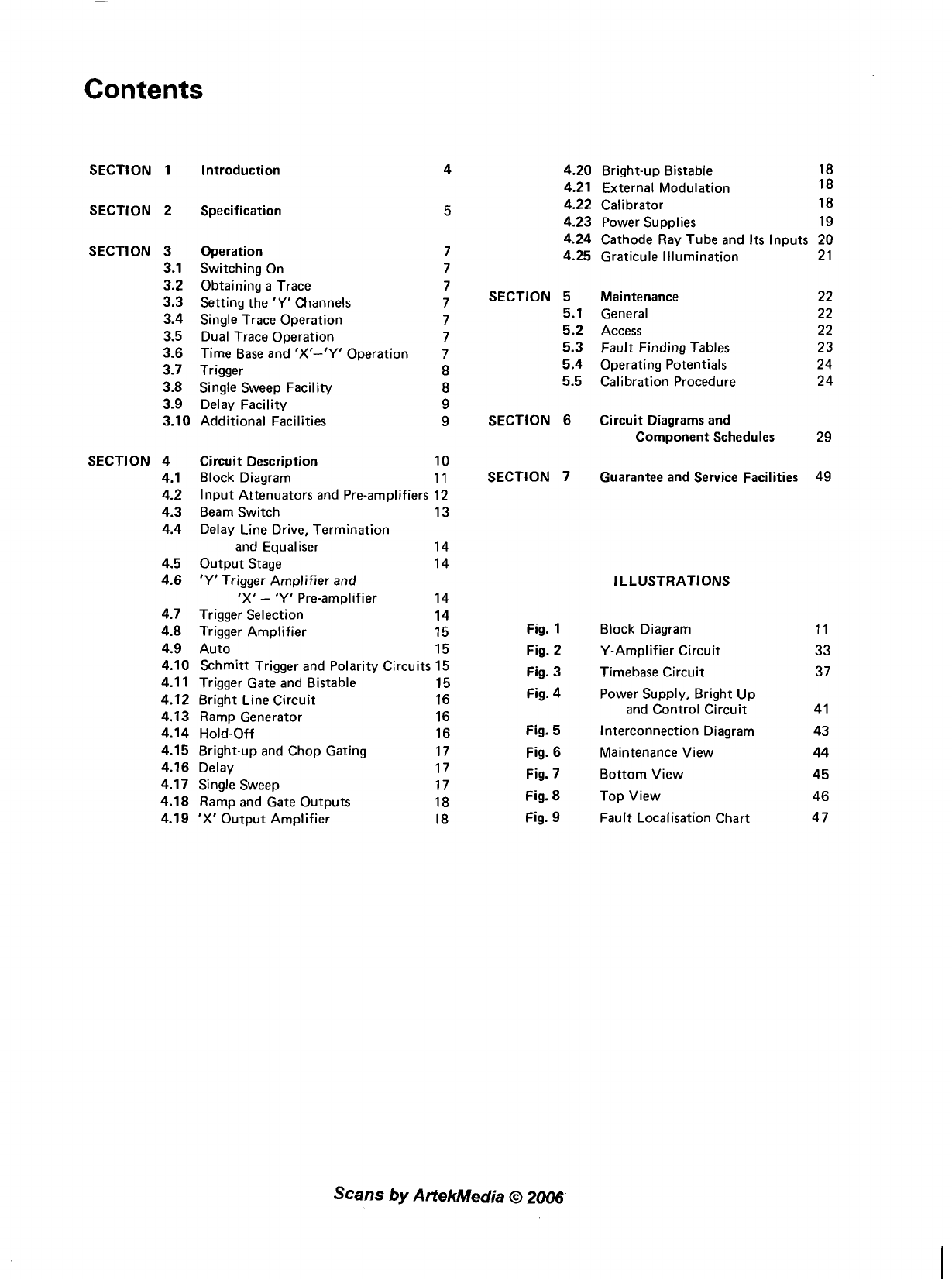
Contents
SECTION
1
Introduction
SECTION
2
Specification
SECTION
3
Operation
3.1
Switchins On
Obtaining a Trace
Setting the
'Y'
Channels
Single Trace Operation
Dual Trace Operation
Time Base and
'X'-'Y'
Operation
Trigger
Single Sweep Facility
3.9
~ela~~acili-ty
3.10
Additional Facilities
4.20
Bright-upBistable 18
4.21
External Modulation 18
4.22
Calibrator 18
4.23
Power Supplies 19
4.24
Cathode Ray Tube and Its Inputs 20
4.25
Graticule Illumination 21
SECTION
5
5.1
5.2
5.3
5.4
5.5
Maintenance
General
Access
Fault FindingTables
Operating Potentials
Calibration Procedure
9
9 SECTION
6
Circuit Diagramsand
Component Schedules 29
SECTION
4
Circuit Description 10
4.1
Block Diagram 11 SECTION
7
Guarantee and Service Facilities 49
4.2
Input Attenuators and Pre-amplifiers 12
4.3
Beam Switch 13
4.4
Delay Line Drive, Termination
and Equaliser 14
4.5
Output Stage 14
4.6
'Y'
Trigger Amplifier and
'Xi
-
'Y' Pre-amplifier 14
4.7
Trigger Selection
14
4.8
Trigger Amplifier 15
4.9
Auto 15
4.10
Schmitt Trigger and Polarity Circuits 15
4.1 1
Trigger Gate and Bistable 15
4.12
Bright LineCircuit 16
4.13
Ramp Generator 16
4.14
Hold-Off 16
4.15
Bright-upand Chop Gating 17
4.16
Delay 17
4.17
Single Sweep 17
4.18
Ramp and Gate Outputs 18
4.19
'X'
Output Amplifier
18
Fig.
1
Fig.
2
Fig.
3
Fig.
4
Fig.
5
Fig.
6
Fig.
7
Fig.
8
Fig.
9
l
LLUSTRATIONS
Block Diagram
Y-Amplifier Circuit
Timebase Circuit
Power Supply, Bright Up
and Control Circuit
Interconnection Diagram
MaintenanceView
BottomView
Top View
Fault Localisation Chart
Scans
by
ArtekMedia
O
2006

Introduction Section
1
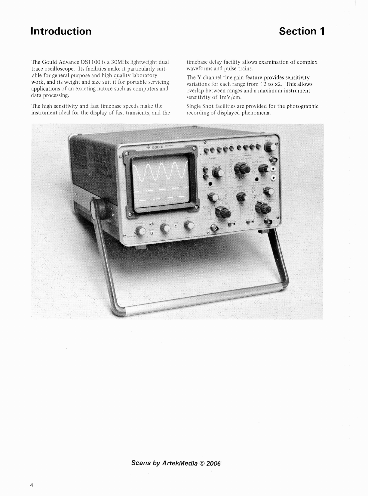
The Gould Advance OS1100 is a 30MHz lightweight dual
trace oscilloscope. Its facilities make it particularly suit-
able for general purpose and high quality laboratory
work,
and
its weight and size suit it for portable servicing
applications of an exacting nature such as computers and
data processing.
The high sensitivity and fast timebase speeds make the
instrument ideal for the display of fast transients, and the
timebase delay facility allows examination of complex
waveforms and pulse trains.
The
Y
channel fine gain feature provides sensitivity
variations for each range from
+2
to
x2.
This allows
overlap between ranges and a maximum instrument
sensitivity of lmV/cm.
Single Shot facilities are provided for the photographic
recording of displayed phenomena.
Scans
by
ArtekMedia
O
2006

Specification Section
2
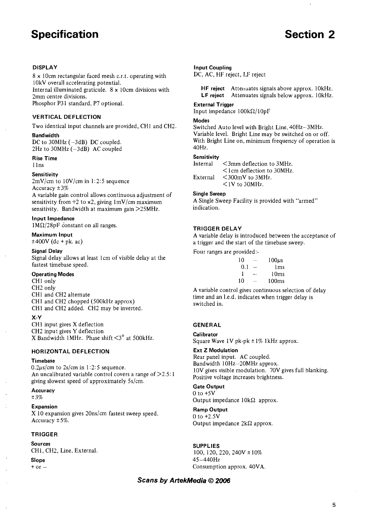
DISPLAY
8
x 10cm rectangular faced mesh c.r.t. operating with
lOkV overall accelerating potential.
Internal illuminated graticule.
8
x lOcm divisions with
2mm centre divisions.
Phosphor P31 standard, P7 optional.
VERTICAL DEFLECTION
Two identical input channels are provided, CH1 and CH2.
Bandwidth
DC to 30MHz (-3dB) DC coupled.
2Hz to 30MHz (-3dB) AC coupled
Rise Time
1lns
Sensitivity
2mV/cm to 10V/cm in 1
:
2:5 sequence
Accuracy
+
3%
A variable gain control allows continuous adjustment of
sensitivity from +2 to x2, giving lmV/cm maximum
sensitivity. Bandwidth at maximum gain >25MHz.
lnput Impedance
1MS2/28pF c'onstant on all ranges.
Maximum lnput
+400V (dc
+
pk. ac)
Signal Delay
Signal delay allows at least lcm of visible delay at the
fastest timebase speed.
Operating Modes
CH1 only
CH2 only
CH1 and CH2 alternate
CH1 and CH2 chopped (5OOkHz approx)
CHI and CH2 added. CH2 may be inverted.
X-Y
CH1 input gives
X
deflection
CH2 input gives
Y
deflection
X
Bandwidth 1MHz. Phase shift <3' at 5OOkHz.
HORIZONTAL DEFLECTION
Timebase
0.2ps/cm to 2s/cm in 1:2:5 sequence.
An uncalibrated variable control covers a range of >2.5: 1
giving slowest speed of approximately 5s/cm.
Accuracy
+
3%
Expansion
X
10expansion gives 20ns/cm fastest sweep speed.
Accuracy
+
5%.
TRIGGER
Sources
CHI, CH2, Line, External.
Slope
+
or
-
lnput Coupling
DC, AC, HF reject, LF reject
HF reject
Atte~~uatessignals above approx. 10kHz.
LFreject
Attenuates signals below approx. 10kHz.
External Trigger
Input impedance 100kfl/10pF
Modes
Switched Auto level with Bright Line, 40Hz-3MHz.
Variable level. Bright Line may be switched on or off.
With Bright Line on,minimum frequency of operation is
40Hz.
Sensitivity
Internal <3mm deflection to3MHz.
<
1cm deflection to 30MHz.
External <300mV to 3MHz.
<
1V to30MHz.
Single Sweep
A Single Sweep Facility is provided with "armed"
indication.
TRIGGER DELAY
A variable delay is introduced between the acceptance of
a trigger and the start of the timebase sweep.
Four ranges are provided:-
10
-
loops
0.1
-
1
ms
1
-
lOms
10
-
looms
A variable control gives continuous selection of delay
time and an 1.e.d. indicates when trigger delay is
switched in.
GENERAL
Calibrator
Square Wave
1
V pk-pk
+
1% 1kHz approx.
Ext Z Modulation
Rear panel input. AC coupled.
Bandwidth 10Hz-20MHz approx.
10Vgives visible modulation. 70V gives full blanking.
Positive voltage increases brightness.
Gate Output
0 to +5V
Output impedance 10kfl approx.
Ramp Output
0 to +2.5V
Output impedance 2kS2 approx
SUPPLIES
100, 120,220,240V
2
10%
45-440Hz
Consumption approx. 40VA.
Scans
by
ArtekMedia
O
2006

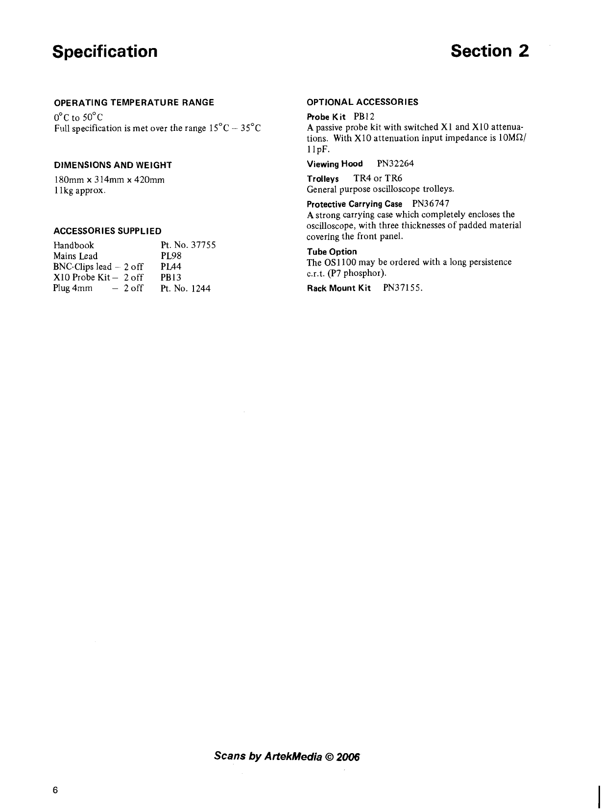
Specification
OPERATING TEMPERATURE RANGE
0°C to 50°C
Full specification is met over the range 15°C
-
35°C
DIMENSIONSAND WEIGHT
180mm
x
314mm
x
420mm
1lkg approx.
ACCESSORIES SUPPLIED
Handbook Pt. No. 37755
Mains Lead PL98
BNC-Clipslead
-
2 off PL44
X10 Probe Kit
-
2 off PB13
Plug 4mm
-
2 off
Pt.
No. 1244
Section
2
OPTIONAL ACCESSOR
l
ES
Robe Kit
PB12
A
passive probe kit with switched X1 and X10 attenua-
tions. With XI0attenuation input impedance is 10MW
1lpF.
Viewing Hood
PN32264
Trolleys
TR4 or TR6
General purpose oscilloscope trolleys.
Protective Carrying Case
PN36747
A
strong carrying case which completely encloses the
oscilloscope, with three thicknesses of padded material
covering the front panel.
Tube Option
The
OS
1100may be ordered with a long persistence
c.r.t. (P7 phosphor).
Rack Mount Kit
PN37155.
Scans
by
ArtekMedia
O
2006

Operation Section
3
3.1
SWITCHING ON
Caution: The OS1100 is convection cooled and must
always be operated in a position such that air circulation
through the bottom and side vents is not restricted.
1. Set the support/carrying handle to the required oper-
ating position. The handle is released by pulling out-
ward both fixing bushes when it can then be turned to
lock in any of 5 positions.
2. Ensure that the supply voltage selector switches on the
rear panel are set to suit the voltage of the supply to be
used and that the corresponding fuse is fitted (see 5.1).
The selector switches must not be operated while the
instrument is switched on. Connect the supply.
THE INSTRUMENT IS INTENDED FOR OPERATION
WITH A SUPPLY EARTH WHICH MUST BE
CONNECTED.
3.
Turn the INTENSITY control clockwise beyond the
POWER-ON setting and ensure that the indicator lamp
lights.
3.2
OBTAINING A TRACE
1. To obtain a trace:-
a) Set the CH1 shift control to approximately mid
setting.
b) Set the MODE switch to CHI.
c) Set the
X
shift control to approximately mid
setting.
d) Set the BRIGHT LINE ON/OFF switch to ON.
e) Set the TRIG COUPLING switch to AC.
f)
Set the TRIG SOURCE switch to CHI.
g) Set the TIMEBASE switch to 5ps.
h) Set the Single Sweep push buttons for normal
operation.
i) Set the TIMEBASE DELAY to OFF.
j) Adjust the INTENSITY control toobtain a display
of the required brightness.
k) Centralise the display by adjusting the CH1 and
X
shift controls.
1) Adjust the FOCUS control and ASTIG preset
control toobtain a sharply defined trace.
3.3
SETTING THE
Y
CHANNELS
1.
Using one of the coaxial input signal leads (PL44)
connect a signal to the CH1 or CH2 input socket.
2. To locate the baseline, set the input slide switch to
GND. At this setting, the input signal is open circuit
and the input of the amplifier is switched to ground.
For vertical movement of the trace, adjust the Y shift
control (identified with vertical arrows).
3.
For:-
4. a) To adjust the Sensitivity
Set the VOLT/cm switch to a suitable setting. To
minimise pickup at sensitive settings it is advisable
to ensure that the ground lead connection is near to
the signal point.
b) If necessary, pull out and adjust the concentric
VARIABLE control. This control allows a range of
sensitivity of approximately t2to x2 about the
calibrated ranges, so that its full adjustment
provides overlap between ranges and a maximum
instrument sensitivity (at reduced bandwidth) of
lmV/cm. An approximate calibrated position is
shown by the broad red band on the front panel
and the accurate calibrated condition can always
be obtained by merely pushing the knob back to
its normal position.
5.
If, under no signal conditions, trace movement is
apparent when the VARIABLE is altered, reset the
BAL preset control.
NOTE:
This control will only need adjustment at infrequent
intervals. Before adjusting the BAL preset control
however, ensure that the input slide switch is set to
the GND setting.
Do not attempt adjustment within the first 15 minutes of
operation to allow internal thermal stabilisation.
3.4
SINGLE TRACE OPERATION
1.
For single trace operation of CHI, set:
a) The MODE switch to CHI.
b) The CH1 shift control (indicated by double ended
vertical arrow) to mid setting.
2. For single trace operation of CH2, set:
a) The MODE switch to CM2.
b) The CH2 sluft control (indicated by double ended
vertical arrow) tomid setting.
3.5
DUAL TRACE OPERATION
In the dual trace condition, the beam switching function
is in operation and results in the independent display of
two signals simultaneously. Two modes of beam switch-
ing
--
chopped or alternate
-
are provided, selected by
the setting of the MODE switch. At any fast setting of
the timebase from 0.2ps/cm to O.Sms/cm inclusive, the
alternate switching mode is recommended. At slow
settings from lms/cm to 2s/cm inclusive, the chopped
switching mode is preferable.
For dual trace operation, set:
a) The CH1 shift control to mid position.
b) The CH2 shift control to mid position.
c) Select ALT or CHOP on the MODE switch.
a')
Direct connection of the input signal, set the input
-
slide switch to DC.
b) Capacitive coupling of the input signal through an
3.6
TIMEBASE AND
X-Y
OPERATION
internal O.1pF 400V capacitor, set the slide switch The sweep speed of the timebase is determined by the
to AC. This allows examination of low amplitude setting of the TIME/CM switch.
a.c. signals superimposed on a high d.c. level. 1. To adjust the time scale of the horizontal axis:-
Scans
by
ArtekMedia
@
2006

Operation Section
3
(a) Set the TIME/CM switch to the required
setting.
(b) If necessary, adjust the concentric VARIABLE
control to reduce the speed.
NOTE
:
The range of the VARIABLE CONTROL is
approximately 3:1. The VARIABLE CONTROL is
uncalibrated. At the CALIBRATED setting only the
calibration corresponds to the setting of the TIME/CM
switch. Selection of the 2sec/cm range and full use of the
VARIABLE CONTROL gives a total sweep time of
approximately 1minute.
2. For horizontal shift of the trace, adjust the X shift
control (identified by a double arrowed horizontal
line above the knob). The control has a COARSE/
FINE action. Initial operation provides coarse shift
control, the return adjustment over a limited arc
provides fine shift control.
3. If a close examination of any portion of the trace, or
the fastest sweep rate, is required operate the PULL
X10 control. In this setting the effective sweep length
is increased to lOOcm and the portion of the sweep
that occupied the centre of the screen will now occupy
the whole of the visible display.
Any portion of this increased sweep length may be
selected for viewing on the display by adjusting the X
shift control. A particular advantage of this facility is
to increase the maximum sweep rate to 20ns/cm.
4. In addition to selection of the speed of the internal
timebase the switch has a functional setting, X-Y. In
this mode the internal timebase is disabled, the display
unblanked and the input to CHI is directed to the X
plates of the c.r.t. while the input to CH2 provides the
Y deflecting signal, irrespective of the setting of the
mode switch.
In the X-Y mode the X channel gain is set to corres-
pond with the CHI deflection sensitivities of the
VOLT/CM switch. The PULL XI0X gain control is
inoperative.
It should be noted that the full range of the X shift
control cannot be used in this mode. To avoid limit-
ation of deflection, the X shift movement should be
limited to retain the spot on the screen when the CH1
input is grounded.
3.7
TRIGGER
Choice of trigger signal source is by one of four push
buttons. These are:-
a) The supply line input frequency derived internally
from one of the secondaries of the supply transformer.
b) CH1 or CH2 amplifiers (these signals are available
irrespective of which beam is being displayed).
c) An external triggering source connected to the EXT.
TRIG. input socket.
The trigger polarity
(+/-)
push button selects the edge
from which the triggering signal is derived.
Movement of the trigger LEVEL control away from the
switched AUTO position allows selection of the triggering
point on the trigger waveform. This allows the start point
of the trace to be set to any point of a waveform.
When the LEVEL control is set to AUTO, the trigger
circuit automatically selects an a.c. coupled mode and
biases to a sensitive level condition. In the absence of a
trigger signal in this mode, the timebase will free run
(BRIGHT LINE) and maintain a displayed, untriggered,
sweep at the selected speed. The AUTO mode should not
be used with waveforms of a wide mark/space ratio.
The BRIGHT LINE mode may also be retained (B/LON)
in the manual trigger condition. Here, when the input
signal is insufficient or the LEVEL control is set for a
trigger voltage beyond the amplitude of the input signal
waveform, the tirnebase will BRIGHT LINE and display
an untriggered sweep at the selected speed.
However this facility can be rejected in the manual trigger
mode by pressing the B/L. ON/OFFbutton to allow
correct operation at low repetition rates of trigger. Auto
or B/L. ON modes should not be used for trigger signals
below 40Hz.
The choice of trigger signal coupling is by three push
buttons as follows, allowing:-
1. A.C. Wide band trigger mode used for most
common triggering signals.
2. D.C. A wideband trigger mode but it is most
useful at very low frequencies. The Y
input coupling must also be d.c. for this
mode to be effective on internal trigger.
2. H.F. Rej. An R.C. filter is switched into the circuit
to reject high frequencies. It is a useful
mode when observing ripple or other low
frequencies in the presence of high
frequency noise or spikes.
4. L.F. Rej.
An
R.C. filter is switched into the circuit
to reject low frequencies. High frequency
triggering may then be effected from
complex waveforms such as those with
high ripple content, or line triggering from
a television video signal waveform.
3.8
SINGLE SWEEP FACILITY
To set the timebase to give a single sweep:-
1. Apply a repetitive waveform and obtain a stable,
triggered, trace with the single shot switch in the
normal (both buttons out) position, by adjusting the
manual TRIGGER LEVEL control.
2.
Press the SINGLE SWEEP push button.
3. Press and release the spring biased ARM push button
The circuit is then primed ready to receive the next
trigger pulse to initiate one sweep. At the end of this
sweep the single shot circuit will be reset, to inhibit
further sweeps, until the ARM push button is again
Scans
by
ArtekMedia
O
2006

Operation Section
3
pressed.
An
1.e.d. indicator shows when the circuit is
primed, awaiting a trigger signal.
NOTE: the Single Sweep function will override the
setting of the BRIGHT LINE facility.
3.9
DELAY FACILITY
In order to examine in greater detail some part of a
complex waveform a delay time may be introduced
between the receipt of trigger and the start of the
corresponding sweep. This allows a faster sweep rate to
be employed, with the effect of magnifying the display
at the point ofinterest. This facility is particularly useful
when looking in greater detail at one pulse in a chain or
one particular line in the video signal in television
receivers, where there is no convenient time-related trigger
pulse close to the area of interest.
To use this DELAY facility:
1. Set up a stable triggered sweep.
2. Switch the DELAY on (the DELAY ON indicator will
light) and increase the range and fine delay control to
bring the required portion of the sweep to within the
first centimetre of the display.
Like the X shift control, the fine delay control has a
dual action which provides coarse setting with wide
movement of the control but fine setting over a limited
arc of return travel.
3.
Increase the sweep rate toexpand the display.
4. Repeat adjustment of the delay time and then the
ramp sweep rate until the required resolution is
obtained.
NOTE:
1. The accuracy and rate of the timebase are unaffected
by any delay setting.
2. There will be a dimming of the display as the effective
duty cycle changes when long delays are used on fast
sweep speeds. This may be corrected by an increase
of INTENSITY.
3.10
ADDITIONAL FACILITIES
3.10.1 USE OF THE PASSIVE PROBE
An
external probe may be used to extend the voltage-
range and increase the input impedance of the Y amplifiers.
The input impedance of a Y channel is 1MR shunted by
approximately 28pF. The effective capacity of the input
lead must be added to this and the resultant impedance
will sometimesload the signal source. Therefore it is
advisable to use a lOMR XI0 probe such as the PB12 or
PB13. This reduces the input capacity and increases the
input resistance, at the expense of the sensitivity. The
probe contains a shunt R.C. network in series with the
input and forms an attenuator with the input R.C. of the
Y Channel. To obtain a flat frequency response it is
necessary to adjust the capacitance of the probe tomatch
the input capacity of the Y Channel as follows:-
(1) Set the Y Channel VOLTS/CM switch to 20mV/cm,
and the TIME/CM switch to0.2msIcm.
(2) Connect the probe to the cal 1V pin just below the
tube face.
(3) Set the adjustable capacitor in the probe tip or
termination with a small trimmer tool for a level
response with no overshoot or undershoot visible
on the display.
3.10.2 CALlV
This pin provides a d.c. coupled positive-going square
wave of 1V
+
1% amplitude at approximately 1kHz
frequency for calibration checks. The square wave has a
source impedance of approximately 20052 and a rise time
of less than 100ns.
Shorting the cal pin to ground will produce a square wave
current waveform of 5mA in the shorting link. This can
be used for current probe calibration.
3.10.3 GATE OUTPUT
This socket of the front panel provides a d.c. coupled
positive-going square pulse of 5V amplitude with a source
impedance of lOkR, the duration of the pulse being
coincident with the appropriate timebase sweep.
3.10.4 RAMP OUTPUT
This socket on the front panel provides a d.c. coupled
positive going timing ramp of
2.5
volts amplitude, with a
source impedance of2kR. The ramp may be used as a
drive for external frequency swept oscillators to allow
display of voltage against frequency.
3.10.5 2-MOD
This socket on the rear panel provides a.c. coupled
blanking to the grid of the tube. Visible modulation can
be seen with an input signal of 10V peak to peak. The
voltage necessary for full blanking is a function of the
INTENSITY setting but is typically 50V, negative going.
The 1.f. input impedance is approx. 800kR. High
frequency input impedance drops to approx. 150a
but this shunt path can be disconnected (see section 4.21).
Scans
by
ArtekMedia
O
2006

Circuit Description Section
4
Figures 2, 3 and
4
show the circuit details of the Y ampli-
fier, timebase and power supplies respectively. Fig.
5
shows their inter-connection but for clarity some details
of this inter-connection are included in the detailed
diagrams also. For convenience, the circuit reference of
any component can be used to determine its location in
the instrument.
1
-
99 Frame or interconnection
100
-
199 CHI Pre-amplifiers,trigger amplifier
beam switch, beam switch bistable.
200
-
299 CH2 Pre-amplifiers, trigger amplifier.
300
-
399 Delay line drive, equaliser, Y O/P
amplifier, bistable drive and X/Y
amplifier.
Trigger Timebase, delay and X O/P
600
-
699
700
-
799) Power Supply
800
-
899 Front Panel Control Board
900
-
999 E.H.T. Supply.
e.g. R309 is part of the Delay Line Drive.
The circuit diagrams are generally arranged for each
printed board assembly or group of boards. These
diagrams include some of the switches, potentiometers
etc., closely associated with the circuit although these
components may be mounted on the frame.
Consequently not all such components appear on the
interconnection diagram Fig.
5
and where it makes the
circuits easier to follow, some components appear on
more than one circuit.
4.1
THE BLOCK DIAGRAM
The block diagram for the complete instrument is shown
in Fig.
1.
It is not intended to be a full working diagram
but gives details of the functional points of the circuit
and their inter-relation. The circuit can be readily
divided into three main sections which are:
Y deflection circuits, X deflection circuits (including
timebase delay and trigger circuits) and Power Supply
which includes Bright-up functions.
Y
CHANNELS
The switched attenuator,pre-amplifier and trigger
amplifier are identical for the two Y channels except
that CH1 provides pick-off and amplification for the X/Y
signal and CH2 provides invert facilities. The selection
of the decade steps of the attenuator and 1.2.
5.
sequence of pre-amplifier gain switching are determined
by the sensitivity selected.
The use of the fine gain facility on either channel allows
a 2:1 increase or decrease in sensitivity.
The channel switch is a fast electronic switch with the
equivalent of a change-over action as shown. It selects
either the CH1 or the CH2 signal to be passed to the sub-
sequent stages and is controlled from a J-K flip-flop. The
state of the flip-flop and hence the channel selection is
determined by d.c.voltages applied to its preset and clear
inputs. In the chop mode, the J-K flip-flop is driven via
its clock input and a signal gate from a free running
monostable, switching the beam between CHI and CH2
signals as the X sweep progresses. In the alternate mode,
end of sweep pulses are fed from the timebase to the J-K
via the signal gate and reverse the beam switch at the end
of each timebase sweep, giving alternate CH1 and CH2
sweeps. In the ADD mode, both the CHI and CH2
switches are closed and the two signals are summed
algebraically. On CH1 or CH2,the appropriate switch is
closed, allowing only that signal to pass.
The signal from the selected channel is passed via a delay
line and amplifiers to the Y deflection plates of the c.r.t.
The delay allows examination of that point in the wave-
form which triggered the sweep since the deflecing signal
reaches the Y plates after the timebase sweep and bright-
up have been initiated.
THE TIMEBASE
The purpose of the timebase system is to generate a linear
ramp to deflect the spot in the X direction. The trigger
system initiates each sweep from the incoming or other
signals, normally to obtain a stationary display of a
repeated waveform.
The internal or external trigger signal as selected is
amplified by the trigger amplifier which is biased by the
required trigger level, and the resultant is amplified and
passed to drive the trigger circuit. If the timebase is
ready to commence a sweep, a transition of the trigger
circuit will set the timebase bistable which in turn initiates
the ramp. This signal is passed via the X amplifier to the
X
deflection plates of the c.r.t.
At the end of the sweep, the bistable is reset, returning
the ramp to the original level. During the period of sweep,
the trigger gate is prevented from passing trigger pulses to
the bistable and this inhibition is maintained by the hold-
off circuit until the ramp generator is fully recovered,
ready for the next sweep to commence on the next trigger
pulse, when the cycle is repeated.
In the delay mode the timebase bistable is triggered in the
same manner but the bistable output to the ramp
generator is inhibited for the period of the delay. To
allow time for the delay monostable to fully reset there
is an additional hold-off control from the delay circuit
into the trigger gate. In Single Sweep, the relevant
bistable normally inhibits the trigger pulses from reaching
the timebase bistable by biasing the hold-off circuit, and
hence closing the trigger gate. When the single sweep
bistable is armed the trigger gate is opened and the next
trigger pulse initiates a sweep. At the end of the sweep
the single sweep bistable is reset, preventing the timebase
from sweeping again until the manual ARM button is
pressed once more.
The trigger signal for the timebase, selected from either
internal, external, or line frequency sources, is passed
through the required processing filter selected by the
Scans
by
Arte


DELAY
LINE Y
O/P
AMPLIFIER
ADD
(CHI CH21
C
ATTEN.
L

Circuit Description Section
4
coupling switch, before being applied tothe trigger
amplifier. The trigger amplifier is biased to the required
trigger level and the resultant amplified output is taken
to the Schmitt trigger to be squared up before being
applied to the polarity circuit.
When Bright Line is selected the output from the polarity
circuit will couple into the bright line monostable. In the
absence of trigger pulses, the bright line circuit will
provide a bias into the trigger gate, causing the timebase
bistable tobe set at the end of each hold off period, thus
giving repeated sweeps for a bright display.
When Auto is selected, in addition tothe bright line oper-
ation being called for, the trigger signal is a.c. coupled and
the amplifier is biased to a sensitive working point.
The bright-up circuits normally hold the c.r.t. beam in the
cut-off state. The output of the timebase bistable, which
allows the ramp to operate, also feeds the bright up circuit
to raise the brilliance of the c.r.t. trace to the level deter-
mined by the intensity control. At the end of the sweep,
the timebase and bright-up bistables are reset, blanking
the trace during the fly back period.
If the
Y
Channels are being switched in the chop mode an
output is fed from the multivibrator via the bright-up gate,
to the bright-up circuits, blanking the trace while the
Y
switching transition takes place.
4.2
INPUT ATTENUATORS AND PRE-AMPLIFIERS
NOTE: The Attenuator and Pre-amplifier in CHI are
identical tothose in CH2. Accordingly, only CHI is
described. The circuit references of all board mounted
components are arranged such that CH1 pre-amplifier
numbers 100-and corresponding components in CH2
200-.
The input signal is applied from the front panel socket
SKA to the
3
position slide switch, S11. when the input
coupling switch is in the D C. position, the input signal is
coupled directly to the input attenuator. In the A C.
position, the input signal passes through C11 which
prevents the d.c. component of the input signal from
passing to the amplifier. The GND position opens the
signal path and connects the input circuit of the amplifier
to ground. This provides a ground reference without
having to disconnect the applied signal from the inllut
connector.
The input attenuators are frequency compensated, voltage
dividers. For d.c. and low frequency signals they are
primarily resistive dividers and the attenuation is deter-
mined by the resistance ratios, the effect of the capacitors
being negligible. However, at high frequencies, the
reactance of the capacitors decreases and the attenuator
becomes primarily a capacitive divider. Each attenuator
contains an adjustable series capacitor to provide optimum
response for the high frequency components and an
adjustable shunt capacitor to set up the input capacity of
each section. The component values in each section are
arranged to provide the required attenuation and present
the same input R.C. characteristic for all settings of the
VOLT/CM switch.
Two attenuator sections are employed to divide by 10and
100respectively. These are used singly or cascaded. The
basic amplifier provides a maximum sensitivity of 2mV/cm,
and gain switching in the amplifier reduces this toprovide
SmV/cm and 10mV/cm sensitivities. The X10 attenuator
is introduced to provide the 20, 50and 100mV/cm ranges;
the XlOO to provide the 200mV, 500mV and 1V/cm ranges
and the X10 and XlOO cascaded to provide the 2,sand
10V/cm ranges.
The X10 attenuator consists of R3and R9. Capacitor,
C13, sets the input capacitance on the 20, 50, 100mV/cm
ranges, while C14 corrects the frequency response of the
attenuator.
The XlOO attenuator consists of R12 and R13. Capacitor,
C16, adjusts the input capacitance on the 200mV, 500mV
and 1V/cm ranges, while C16 corrects the frequency
response of the attenuator. Capacitor, C19,provides
adjustment for the input capacity when the attenuators
are not in circuit. R18 determines the input resistance of
the oscilloscope when the attenuators are not in circuit
and forms part of the attenuator resistors on all other
ranges.
The output from the attenuator is taken via the input
current limiting resistor, R17, to the gate of the field
effect transistor, TRlOl(a). The input stage consists of
two transistor feedback pair amplifiers, TRlOl(a)/TR102
and TR101(b)/TR103, connected as one differential
amplifier. The overall gain of each stage is determined
by the ratio of the feedback resistor, R111 or R112, to
the common source resistor, R40. The single ended input
to differential output gain in this arrangement is approxi-
mately 5 with S13 in the CAL position.
The signal input is fed to the gate of TRlOl(a) and
balancing potentials to the gate of TRlOl(b). These
transistors are matched and in a common encapsulation,
therefore any drift due to temperature changes will be
minimised.
The gain of the stage is a function of the common source
resistance, hence the VARIABLE GAIN function is avail-
able when R42 and the variable control potentiometer,
R2, are switched into the circuit.
The field effect transistor gives a high input impedance
which does not shunt the attenuator significantly. The
signal excursion at the gate of TRlOl(a) is restricted by
the limiting diode, D102, which is returned to the negative
supply line. Differential signals from the input stage are
fed via R119 and R121 to the gain switching stage, TRIO41
TRIOS. A potentiometer, R120, is provided to supply a
small balancing current into the source of TRlOl(b). This
gives some variation of the collector potential TR102/103,
and allows the emitter potentials of the following stage to
be equalised to prevent trace movement when gain
switching.
Scans
by
ArtekMedia
O
2006

Circuit Description Section
4
Gain switching is achieved by S12dB, switching resistance,
R116, R117 or R118, between the emitters of TR104 and
TR105 to give the 2mV, 5mV and 10mV/cmsteps.
Trimmer capacitors are provided for high frequency com-
pensation. Decoupled resistors, R127 and R128, are
included to reduce collector dissipation and keep thermal
drift to a minimum. The collector supply is stabilised by
the 4.3V Zener, D103.
4.3
BEAM SWITCH
The CH1 and CH2 signals feed two identical long-tail
pair amplifiers, TR15112and TR15314, on the beam
switch printed circuit board. In addition to providing
signal current feed to the beam switch, provision is made
for overall gain adjustment in each channel by means of
the two networks. R1511152 and R1611162. C151 and
The beam switch for each channel consists of an array of
four transistors arranged in common base configuration.
The transistors are connected in pairs with their emitters
commoned. One collector of each pair is returned
directly to the supply and the other collector to the
common output load. The base of each transistor in the
array is returned via a potential divider to an output from
the
J-K
flip-flop, IC153, which will either be 'HIGH' or
'LOW' dependhi on the drive at its preset, clear or clock
inputs. This gives the facility for turning on or off each
transistor in the array and thus diverting signal current
into the load or into the supply rail. Signal feed to each
common base pair comes from the preceding stage and
the shift network also is connected between the common
emitters of each pair.
C152 are included to a~6wthe h.f. response of the two Thus, assuming CH1 is to be selected, Pin 15 on the
J-K
channels to be matched. A.O.T. resistor, R199, gives the will be 'HIGH' and Pin 14 'LOW'. In IC151 transistors
facility for balancing the currents in CH2 to minimise (3-4-5)and (9-10-11)will be turned on,diverting signals
trace shift when the INVERT switch is operated. to the load. Transistors (1-2-3)and (6-7-8)will be off.
TABLE SHOWING VOLTAGES INBEAM SWITCH CIRCUIT
MODE
Notes: Via R190 ViaR187
Circuit
Reference
IC151
IC152
TR157
TR158
IC155
-
LOW (IC1511152)
=
-0.35V W.R.T. GND
HIGH(IC1511152) =-0.04V
Equivalent points on IC153, logic using 1Vto -4.6V
PIN No.
5
2- 1Q
4-1Q
6-1~
9-1Q
2- 1Q
4- 1Q
6- 1Q
9-la
COLL
COLL
2 1PR
3 1CL
Scans
by
ArtekMedia
O
2006
CH1
3
4
L (0)
H (1)
L (0)
H (1)
H (1)
L (0)
H (1)
L (0)
H (OV)
L (-5.3V)
L(O)(-5.3V)
H (1) (OV)
CH2
3
4
H (1)
L
(0)
H (1)
L (0)
L (0)
H (1)
L (0)
H (1)
H (OV)
L (-5.3V)
H(l)(OV)
L
(0) (-5.3V)
CHOP
H (OV)
L,-5.3V)
H(l)
(-5.3V)
ALT
H (OV)
L,-5.3V)
ADD
L(0)
H (1)
L (0)
H (1)
L(0)
H (1)
L(0)
H (1)
H (OV)
L (-5.3V)
L(-4.7V)
L (4.7V)
X-Y
3
4
H (1)
L (0)
H (1)
L (0)
L (0)
H (1)
L (0)
H (1)
L (-5.3V)
H (OV)
H(0V)
L (-5.3V)

Circuit Description Section
4
In 1C152 transistors (3-4-5) and (9-10-11) will be "off
',
transistors (1-2-3) and (6-7-8)will be "on", diverting
signals away from the load and into the supply rail. The
state of the J-K is determined by the position of the
MODE switch, S152,the wiper of which is normally held
at -5.6V via TR158,being held on through R185 and
R188. Since the 1C 153is operated between ground 2nd
-5V returning any preset or clear input to the MODE
switch wiper via a diode will be equivalent to a 'LOW'
state at that input and set the J-K to the appropriate
condition.
In all modes except chop,TR315 is held "on" by the net-
work, R365, D305 and R364. This returns R362 to
ground, holding the multivibrator, TR3
131314,in a
quiescent state.
When CHOP is selected, TR315 is turned off and the
miltivibrator free runs at approximately 1MHz. Output
from the multivibrator feeds the two transistor gate,
TR3
111312,and then to the clock input of the J-K.
Alternate pulses are also fed into the gate from the time-
base and in the CHOP mode turn the gate 'OFF' during
the flyback period. This inhibits beam switching during
the flyback period and minimises the effect of chop
interference on the trigger circuitsjust prior to the start
of sweep. Chop pulses are also fed to the bright-up circuit
to blank the switching transitions.
When ALT. is selected, TR312is turned off and alternate
pulses only are fed to the gate and these clock the J-K at
the end of each sweep.
When ADD is selected both preset and clear are taken
'LOW' via diodes D160and D161,thus taking Pins 14and
15on the J-K 'HIGH'. This turns all transistors in the
arrays on, feeding signal currents from both channels to
the common load. In order to prevent upsetting the shift
control d.c. conditions transistors (1-2-3) (6-7-8)on lC151
are turned off by pulling their bases negative via R190 and
D159. Similarly transistors (1-2-3) (6-7-8) on IC152 are
turned off by pulling their bases negative via R187 and
D159.
In order to avoid upsetting the common load d.c. condit-
ions two current sources, TR155/156 are turned on to
remove the excess d.c. current via diodes, D1521153.
When the X-Y mode is selected, the tirnebase range switch
connects +lOV to the base of TR157 via R191, turning it
on and TR158 off. Since TR157 is saturated, diodes,
R308 are arranged to match the characteristic impedance
of the balanced printed circuit line which introduces a
signal delay of approximately 100ns. This ensures that
the trigger point of the signal is always visible on the
screen.
The output of the delay line is terminated by the resistors,
R310and R311, and feeds into a common base stage,
TR303/304. The network, R348, and potentiometer,
R349, allow for any small matching adjustments necessary
due to manufacturing tolerances in the line.
The pulse response for the uncompensated delay line can
be represented by a fast rise for about 50% of amplitude
followed by a considerably longer rise to full amplitude.
Correction for this response is provided in part by net-
works C3291R340, C301/C330/R350, C302/R301 in the
delay line driver stage, and also by the following stage
TR305/TR306 which in addition raises the signal level to
that required to drive the output stage.
4.5
OUTPUT STAGE
The output stage consists of four transistors, TR307,
TR308, TR309,TR310,operating as a differential
cascode amplifier. High frequency compensation is
provided in the collector circuits by L301 and L302 and
in the emitter circuit by the networks, C313/R369and
C331/C315/R330.
The outputs are taken to the Y deflection plates via Zener
diodes, D302 and D303, which raise the Y mean plate
potential by 33V.
4.6
Y TRIGGER AMPLIFIER AND X/Y
PREAMPLIFIER
The trigger amplifier consist of long tail pairs, TR106/
TR107 and TR206/TR207 receiving differential signals
from the emitter circuits of the beam switch driver stages
and providing a single ended output for the timebase.
R135 and R235 allow the d.c. level on CHI and CH2
outputs tobe set to OV.
An additional output is taken from the CHI trigger
amplifier and fed to an amplifying and inverting stage,
TR3
16. This provides an output level of approximately
60mV/cm and feeds CHI signals to the X amplifier when
the X-Y MODE is selected. The gain of this stage is set
by R373 and phase shift correction is provided by C327
across the feedback resistor, R374.
D155, are returned to 5.3V, this is the condition for
selecting CH2 and ensures that in X-Y CH2 always
4.7
TRIGGER SELECTION
becomes the Y deflection irrespective of the setting of The trigger signals from CHI, CH2, Line and Ext. are
the MODE switch. taken to the push button source selector, S401 to 404.
The two internal trigger signals are brought from the Y
unit via 50acoaxial cable-andterminated by resistors,
4.4
DELAY LINE DRIVE, TERMINATION AND
R405 and R406. The line trigger signal is derived from
EQUALISER
one of the supply transformer secondaries and attenuated
Signals from the beam switch pass to the delay line driver, to the correct level by resistors, R402 and R404. The
a further long-tailed pair, TR301/302,fed from a constant external trigger input, SKE, is connected to S401 via the
current source, TR316. The collector loads R307 and attenuator network, R401, C401 and R403.
Scans
by
Artekhledia
O
2006


Circuit Description Section
4
signal applied to its base from TR421 will stop it conduct-
ing. Its collector voltage will rise and the cross coupling
components, R490 and C423, will turn on TR419. The
common emitter potential of the two transistors will rise
with the base of TR419,holding off TR420. The collec-
tor potential of TR419 will fall allowing the ramp gener-
ator tosweep. The negative going ramp is returned via
D422 and R491 to the base of TR419. The point at
which TR419 turns off and the bistable resets to normal,
determines the end of sweep.
Transistor, TR422,forms a buffer on one output from
the timebase bistable, via TR428. From this buffer stage
outputsare taken toreset the single sweep circuitry, see
Section 4.17, and toprovide the alternate pulse, being
used to operate the channel switch in the ALTERNATE
mode. See Section 4.3.
4.12 THE BRIGHT LINE CIRCUIT
If, in the AUTO or BRIGHT LINE mode, the trigger
simal for the timebase is lost or becomes too small to
trigger reliably, the bright line circuit causes the timebase
to free run by applying a positive bias into the trigger gate.
In this condition a bright trace is produced irrespective of
the timebase speed selected.
Transistors, TR408 and TR409, form a monostable circuit.
In the quiescent condition both transistors are off.
Negative going trigger input pulses from the polarity
circuit via D401, are differentiated by C410 and applied
to the base of TR408. The collector potential will rise,
with
it the base and emitter potential of TR409. The
charge on capacitor, C4 12,will hold TR408 conducting
(by the time constant, C412 and R438). With the emitter
potential of TR409 high, TR410 is held off, therefore
giving no bias into the trigger gate. However, with no
trigger pulses into TR408 the emitter of TR409 will fall
to a low potential, so that TR410 turns on, thereby giving
a positive bias into the trigger gate.
The action of the monostable is controlled by the diode
gate, D401 and D404. D401 is reverse biased, inhibiting
trigger input signals if D404 is grounded at Pin 8. That is
if the transistor switch, TR407, is conducting (S3b closed
in Manual) and S408 is closed (B/Line off). In the Single
Sweep mode Slainhibits bright line by directly grounding
Pin 8.
4.13 THE RAMP GENERATOR
The basic bootstrap ramp generator is formed by f.e.t.,
TR441, as a source follower, and the subsequent emitter
follower, TR442, with a constant current load, TR443.
This constant current produces across the Zener diode,
D432, a constant voltage difference from the gate poten-
tial of TR441. A portion of this voltage is taken from the
wiper of R548 and fed back to the gate of TR44
1
via the
selected timing resistor, RT.
drop linearly. This linear ramp, whose rate is set by the
values of RT and CT and the variable sweep control,
R548, is fed from the emitter of TR442, via S6cb to the
X
output amplifier and hence the
X
deflection plates of
the c.r.t.
In the quiescent state, the ramp voltage is held positive by
the collector current of TR435 flowing through diodes,
D430 and D437, the whole being maintained at balance
by the differential amplifier pair, TR437/TR438.
When the timebase bistable is set,the collector voltage of
TR419will fall, turning on TR434. Transistor, TR435,
will turn off, thereby reverse biasing diodes,D430 and
D437, and allowing a negative-going ramp to commence
under the influence of the voltage across RT. The ramp
will continue to run negatively until the bias applied to
the base of TR419 in the timebase bistable, via the poten-
tial divider, R491and R485, causes it to turn off, where-
upon the timebase bistable will assume its reset state, with
the collector potential of TR419 high. Transistors, TR434
and TR435, will also assume their original states, with
TR435 conducting hard causing diodes, D430 and D437,
to conduct, thereby charging the timing capacitor toits
original positive potential. Since this flyback current is
many times greater than the ramp current through the
timing resistor RT, the flyback time is short compared to
the ramp time. When the ramp potential reaches the
quiescent level, TR438 will conduct, reducing the current
in TR435 to balance the current in RT.
4.14 HOLD-OFF
Triggering of the timebase bistable must be prevented or
held off during the flyback period until the ramp generator
has fully returned to its quiescent state. When a trigger
pulse passes through the trigger gate and initiates a sweep,
the ramp voltage applied to potential divider, R539 and
R540, starts tomove negative. This change is coupled via
D43
1
to the base of transistor, TR440, which will turn
off. Its collector potential rises and the clamp transistor
in the trigger gate circuit, TR429,turns on, due to base
current through R612, and inhibits any further trigger
pulses passing to the base of TR42
1.
The selected hold off capacitor ChO, is connected to the
base of the transistor, ~~440,and ischarged by the
negative going potential of the ramp applied via diode,
D431. At the end of the sweep when the ramp is reset
this diode will be reverse biased and subsequently the base
potential of TR440 will rise slowly under the influence of
ChO and resistor, R532, as the capacitor charges toward
+10V. After a period the transistor will turn on, causing
its collector potential to fall, and turning off the gate
clamp transistor, TR429. This delay or hold-off period
allows time for the ramp generator to reach itsoriginal
In the absence of other influences, the resultant constant quiescent state before any further trigger pulses can be
current flows toground through the selected timing passed by the trigger gate. The hold-off capacitor is
capacitor, CT, causing the voltage across this capacitor to selected by S6bb and is the next smallest timing capacitor.
Scans
by
Artekhledia
O
2006

Circuit Description Section
4
4.15 BRIGHT-LIP
and
CHOP GATING
(DRIVESIGNALS)
The display is brightened up during the sweep by unblank-
ing the c.r.t. The drive signal to the bright-up bistable is
derived as follows.
The collector voltage of TR419 is coupled to TR428,
which with TR430 form a cross coupled stage. The base
of TR430 is biased by resistors, RSOS, R506 and R494,
to a lower voltage than the threshold of the ramp start
pair, TR434 and TR435. This allows the ramp to be
initiated before the bright-up circuitry, so avoiding any
interference at the start of the sweep. The output from
the collector of TR430 is added to the chop transition
blanking voltage obtained via the emitter follower, TR43
1.
The chop blanking voltage is necessary toblank the dis-
play during the successive transitions between CH1 and
CH2 when operating the Y system in the CHOP mode.
The summed output is passed to the Bright-Up circuitry.
(See section 4.20.)
4.16 DELAY
In this mode a delay is introduced between the acceptance
of trigger and the commencement of the sweep and assoc-
iated bright-up signals. The delay circuit consists of a
monostable, comprising the cross coupled common
emitter pair, TR423 and TR427,with the associated
emitter followers, TR424 and TR426. The timing capaci-
tor, CD, is selected by S5 and is connected between the
collector of TR423 (via emitter follower TR426) and the
base of TR427.
The delay time is determined by the current from the
current source transistor, TR439, and is adjustable over a
10:1 range, set by the potentiometer, R536 and R537
-
the coarse and fine delay controls. The monostable is
triggered by a pulse from the collector of TR420,in the
timebase bistable which is differentiated by C422, tothe
base of TR423. This will cause TR423 to conduct and,
via the cross coupling, turn off TR427. The base of
TR427 will slowly rise positively as CD is charged by the
current source, TR439. At the threshold voltage the
original state will be resumed, with TR423 turned off and
TR427 conducting. The diode, D424, allows a fast re-
charge of CD.
he
timebase inhibit control is taken from
the collector of TR427, which is at a 'high' potential, via
emitter followers, TR426 and TR425, to the collector of
TR419 in the timebase bistable. Transistor, TR425, acts
as a clamp on the collector swing of TR419, preventing
the downward excursion which would initiate the ramp
and bright-up circuits.
Transistor switch, TR452, is normally held off by S5c but
in the delay mode it conducts when TR420 is on. When
TR420 turns off on receipt of a trigger signal, TR452 is
slow in turning off, maintaining a clamp on the collector
of TR419 until maintained by TR425. This prevents a
false start of sweep at the beginning of the delay period.
the base voltage of TR425 will fall. As thishappens the
collector voltage of TR419 will drop, thus initiating the
ramp.
A finite time must elapse following the delay period for
the delay timing capacitor to completely discharge before
a second delay can be triggered. This hold-off period is
achieved as follows. During the delay period the positive
output from the emitter follower, TR426, is taken, via
emitter follower, TR432, to discharge the capacitor, C.ho.
At the end of the delay period when the input voltage to
TR432 falls, the voltage across thishold-off capacitor will
fall only slowly, therefore introducing some delay before
transistor. TR436,can start conducting. The potential on
the collector of TR436 is taken via emitter follower
TR454 as a hold-off voltage to the base of the hold-off
transistor TR440. Its action is the same as a ramp input
to the trigger gate as described in Section 4.14. Transistor,
TR453, acts as an input clamp to overcome trigger pick-up
during the delay period. Switch SSaf either eilergises the
DELAYION warning light, D422, or,in the delay OFF
condition, biases the input of the monostable, via R495,
preventing any trigger pulses from initiating a delay.
4.17
SINGLE SWEEP
In this mode, a hold-off bias is applied to TR440 and
hence the trigger gate, thereby inhibiting trigger pulses
from reaching the timebase bistable. When the ARM
button is pressed this bias is removed and the next input
trigger pulse will initiate a single sweep of the ramp. At
the end of the ramp the reset action of the timebase
bistable will set the single sweep circuitry, applying the
inhibiting bias tothe hold-off circuit, preventing a further
sweep until the ARM button is pressed again.
The single sweep circuitry is contained within a dual
bistable positive edge operated c.m.0.s. integrated circuit,
IC402, which operates between the OV and -lOV lines.
The first bistable operates as a slave, following the action
of the ARM push button without any bounce interference,
while the second bistable controls the bias applied to the
hold-off circuit. The output from this second bistable
(Pin 12) is normally at OV, with no resultant effect on the
oueration of the timebase.
Operation of the Single Sweep push button, Slb, removes
the high (OV) input from Pin 10(the reset input of the
second bistable).
At the end of the next sweep the timebase bistable is reset
in the normal manner (see Section 4.1I), the collector
potential of TR419 rises, causing the collector voltage of
TR428 to fall. This fall is coupled via Zener diode, D435,
to the base of TR422. Therefore,at the end of the sweep
the collector potential of TR422 will rise giving a positive-
going edge which, via R610 and C441 is applied to the set
input of the single shot (second) bistable, causing (Pin
12)todrop to -10V, D429 conductsvia R594,re-applying
the hold-off bias to
TR440 and preventing further sweeps.
At the end of the delay period, transistor, TR427, will It also applies a high voltage via S2 to Pin 6. (The Set
conduct, causing its collector potential tofall, similarly input on the first bistable.) This connection drives the
Q
Scans
by
ArtekMedia
O
2006

Circuit Description Section
4
output (Pin 2) low, causing no change of state on the
second bistable. Operation of the ARM button applies a
high voltage while pressed to the reset input (Pin 4) of
this slave bistable, giving a correspondinghigh output at
Pin 2. Releasir~gthe ARM button transfers the high input
from the reset to the set input (Pin 6)of the slave bistable
causing the output
Q
to be set low again. This high
voltage applied to the clock input (Pin 11)of the second
bistable, allows to rise to OV therefore removing the
hold-off bias. This then allows the next input trigger
pulse to initiate one sweep.
At the end of the sweep the second bistable is again set
via C441 to inhibit further sweeps until the ARM button
is operated again.
While the bistable is armed the output from Pin 12is high
and emitter follower TR449 turns the 1.e.d. (D434) on.
As the output returns to -lOV this 1.e.d.ARM indicator
is extinguished.
4.18 RAMP AND GATE OUTPUTS
An
output from the ramp generator is coupled into transis-
tor, TR444. This inverting stage gives an output which, via
Zener diode, D441,will swing linearly from ground poten-
tial to approximately +2.5V as the ramp moves across the
c.r.t. face from left to right. The gate output pulse is
taken from the collector of TR434,via R516 and consists
of a positive pulse from ground to approximately +5V,
present during the ramp period.
4.19 THE X OUTPUT AMPLIFIER
The signal selected by S6cb, either the linear ramp as
provided by the ramp generator,or the output of TR316
(the horizontal deflectingsignal from CHI in the X-Y
mode), is taken to the base of TR445, one half of a long
tailed amplifier, TR445 and TR451. The emitter resistor
of this stage can be reduced in value to give the X10 gain
increase necessary in the 'Pull X10' X condition. The X
shift voltage, derived from the shift control potentiometers,
R591 and R592, is taken via emitter follower, TR456, to
the other input of the long tailed amplifier. R567 and
C440 provide high frequency compensation in the X10
mode. The differential output from this stage is taken via
emitter followers, TR446 and TR450, to the bases of the
long tailed output stage, TR447 and TR448. The outputs
to the X deflection plates of the c.r.t. are taken directly
from the collectors of these transistors. The gain of this
stage being determined by the collector load resistors,
R571 and R579, and the parallel/series emitter resistor
network of R577 and R574/R580. R576 and C442
provide high frequency compensation.
4.20 THE BRIGHT-UPBISTABLE
TR704 and TR705 form a bistable switch, which is slave
to the bright-up input applied via C736 from the timebase.
Its function is to control the grid to cathode potential of
the c.r.t. The network, R725, C738, R726 and D713,
turns on TR705 when the instrument is switched on,
ensuring that the bistable is the bright-up state. The
bistable operates at low voltage in order to improve speed
and provides a low impedance source to the output stage.
This voltage is defined by D716. Drive to the output
stage transistor, TR706, is fed by the network, R733,
C741 and R732, C740, whose function together with
D714 is to prevent TR706 from saturating. When the
voltage between the collector and emitter of TR706
drops to about 1.5V, D714 conducts and limits the base
current of the transistor. When TR706 and TR705 are
conducting the cathode of the tube is most negative and
the tube is then in the bright-up mode. When TR706 is
switched off, as the bistable switches over, R737 holds
the collector positive, and the tube is blanked off. The
voltage swing at TR706 being approximately 50V.
During turn off, TR707 turns on to speed up the edge
with a differentiated signal applied via C742. The bright-
up bistable modulates the cathode directly, and operates
at between
-
1425V and 1375Vwith respect to ground.
A supply for this circuit is provided by BR702 and C734.
The e.h.t. voltage is developed across the coupling capaci-
tor, C736, and R730 holds pin 712 safely at ground if the
input lead is disconnected. Input from the timebase to the
bistable is from the emitter of TR431(on the timebase
board), where the chop blanking and 'end of sweep'
blanking signals are summed.
4.21 EXT.
Z
-
MODULATION
External Z-modulation is applied via the 4mm sockets,
SKH and SKJ, on the rear panel of the instrument. This
signal is applied directly to the grid of the tube via the
capacitor, C725. R712 and R713 effectively define the
input impedance at the grid at about 800kS2. D706 is
used to prevent the incoming signal from driving the grid
positive with respect to the cathode voltage. An excessively
negative voltage at the grid is also prevented by the break-
down action of D706. R716 is used to limit the peak
modulation drive current in either of these modes, with
C727acting as an h.f. by-pass capacitor. R715 provides a
bIeed current to discharge C725 and so prevent any
voltage appearing at the input sockets. R742 and C726
provide an h.f. by-pass network which is used to decouple
the grid against movement when the normal bright-up
waveform is applied to the cathode. The capacitive load
of this network reduces the h.f. input impedance seen at
the
Z
MOD sockets, although it is assumed that the driving
source impedance will be low when the frequency is such
that the network begins to load the input. In applications
when h.f. Z MOD input impedance is important, this net-
work may be disconnected by removal of R742 which is
soldered on pins on the rear panel p.c.b. Access is avail-
able by removing the top cover.
4.22 CALIBRA'TION
This circuit is situated on the front panel control board
assembly. TR802 and TR803 form an emitter-coupled
multivibrator with C804 acting as the timing capacitor.
The collector current of TR803 is used to turn TR804
on and off and with the series chain, R820-821,provide
Scans
by
ArfekMedia
O
2006

Circuit Description Section
4
a
1V peak to peak positive-going square wave at point
803. R819 is used to accurately set this voltage. The
values in the chain are selected such that a 5mA current
is available when the output pin is shorted to ground.
4.23
THE POWER SUPPLIES
The OS1100has seven supply lines, +150V, +75V, +50V,
+10V, 10Vand two e.h.t. lines,
-1
500V and +8.5kV.
The +10V and -lOV and the two e.h.t. lines are fully
stabilised; full current protection exists on the 10V
supplies and a partial protection on the e.h.t. lines. The
remaining lines are unstabilised and are protected by the
supply fuse, FSl. All supplies are obtained from the
secondaries on transformer, TI,with the mains input
selected switches, S10and S9, on the rear panel of the
instrument. In the 240-220 voltage input range the two
primaries of the transformer are connected in series, with
a selection being made on the 100Vtap on one of the
primaries for the 220V connection. For 1OOV and 120V
supplies the primaries are effectively paralleled. In the
case of the lOOV connection the supply is applied across
the 0-100V taps on the tapped primary; the 120V tap on
the same winding then produces a boosted voltage which
is used to supply the other primary winding.
Mains supply is applied via the connector, SK
G.,
on the
rear panel of the instrument.
4.23.1 +10V
and
-10V
LINES
A 26V r.m.s. centre tapped supply is rectified by BR703
and smoothed by C719 and C720. This provides
+
16V
d.c. and 16Vd.c. which is fed toeach of the IOV supply
regulators. The 16Vsupplies are also used to provide
power for the graticule illumination circuit on the front
panel control board. In addition,at point 719 part of the
a.c. supply is fed via R702 toproduce the line trigger
signal for the timebase.
Two integrated circuit regulators provide the 10V
supplies and incorporate internal current limits and
thermal overload protection. The integrated circuits give
nominally 8Vbut are arranged to give 10V with the aid of
the divider network, R7181R717, for the +10V line and,
R719/R720, for the -lOV line. C721 and C722 provide
decoupling at the ground pin of the regulator tomaintain
the ripple rejection of the circuit. R743 and R744 are
A.O.T. resistors which are used to set the 10Voutput to
within 2200mV. D711 is a protection diode to ensure
that latch up conditions do not occur during switch on.
These 10Voutputs are taken to SKLto feed the Y ampli-
fier and timebase, and SKM to feed the front panel control
board. C723 and C724 provide local supply decoupling at
these output sockets.
4.23.2 +150V, +75V
and
+50V
SUPPLIES
The +150V and +75V supplies are used to provide power
for the timebase and Y-amplifier deflection circuits. A
64V r.m.s. supply from the transformer is applied via
points 707 and 717 to D708, D709, C717 and C718
which comprise a voltage doubler circuit of which D709
anode is made the earthy connection. Outputs across
C718and C717are +75V and
+
150Vrespectively. A
resistive bleed, R721, is used to discharge C718 when the
instrument is switched off. Outputs from these supplies
are fed to SKLand SKM for the Y-amplifier, timebase and
front panel control board.
The +50V supply is used to provide the supply for the
bright up circuit and is held at the cathode potential,
that is, with the negative connection at -1425V (see
Section 4.20on description of bright-up bistable circuit).
A 38V r.m.s. input is applied via points 710 and 711 to
provide 50V d.c. with the bridge rectifier, BR702, and
smoothing capacitor, C734.
4.23.3
E.H.T.
SUPPLlES
Two e.h.t.supplies are provided for the cathode ray tube,
-1500V for the gun and +8.5kV for the p.d.a. giving an
overall accelerating voltage of 10kV. Both suppIies are
derived from a tapped winding on the transformer, with
the p.d.a. supply being obtained by a quadrupler circuit
comprising diodes, D901-904, and capacitors, C901-4.
R901 is a series resistor for protection purposes to limit
the maximum fault current available from the multiplier.
R902 and R903 form a resistive bleed to discharge the
multiplier when the instrument is switched off. The
current from R903 supplies the bias current requirements
for the e.h.t. regulator circuit.
The gun supply is derived from the 1300V r.m.s. tap on
the transformer which is rectified and smoothed by D710
and C706-710to form a
-
1510Vsupply. Further
smoothing is achieved by R701 and C711-715 to provide
a line with reduced ripple voltage.
Stabilizationof both e.h.t. lines against supply variations
is achieved as follows:
-
One end of the e.h.t. winding feeds the rectifier diodes
in the normal manner, the other end is connected to
ground via bridge rectifier, BR701. The alternating
current in the winding passes through BR701
/TR701,
TR702, R703, R740 as a direct current which develops a
d.c. voltage across C701 and C702. Over voltage protec-
tion of these components is achieved by a chain of Zener
diodes, D701-3. This d.c. voltage controlled by the
conduction of the cascode connected pair ot transistors,
TR701 and TR702, is subtracted from the peak voltage
available at the 'hot' end of the winding; thus by varying
the conduction of TR702 the rectified high voltage
supplies can be controlled.
The stabilising circuit operates at the negative peak of the
waveform from the e.h.t. winding, when current flows
from the low side of the winding through Pin 716 and the
bridge rectifier, BR701, to OV. Conduction in the bridge
holds the negative side of C703, C704 etc. near OV.
Consequently, for balanced working conditions, potentials
at the base of TR702,the emitter of TR703 and hence the
base of TR703,must also be near OV. In fact the diode
or base-emitter junction voltage drops in TR703,D704,
TR702 and BR701 cancel each other. If the feedback
current from the -1500V supply through R710is not
exactly cancelled by that defined by R706 and the preset
Scans
by
ArtekMedia
O
2006

Circuit Description Section
4
control, R707, from the t10V supply, the base potential
of TR703 will differ from OV. The conduction of TR701
and TR702 will vary the voltage across C701 and C702 to
correct the
-
1500V supply level.
At this same peak of the supply cycle, current from the
e.h.t. multiplier, via R903 flows via D705 defining the
base potential of TR701 just above t10V so that TR701
operates in cascode from TR702. At other points in the
cycle, D704 and D705 are reverse biased, and capacitors,
C701-4,retain the relevent operating potentials of TR701
and TR702. When the posit&e peakoutput from the e.h.t.
winding is reached, the same correction voltage across
C701 and C702 is subtracted and first order stabilization
is applied to the t8.5kV p.d.a. supply. A small additional
current from the t150Vline via R741 supplements the
base current requirements of TR701 and TR702.
4.24
CATHODE RAY TUBE AND ITS INPUTS
The OS1100 employs a mesh p.d.a. tube with a high
efficiency aluminised screen.
The interconnection diagram, Fig. 5. shows the connec-
tions to the various electrodes for the alternative types of
tube used, D14-280 and D14-120.
4.24.1 THE GUN
The beam current and hence the spot intensity is
controlled by the differentialpotential between the grid
and cathode. In the bright-upmode the cathode supply
is derived directly from the -1.5kV stabilised line via
D707. Thus the effective voltage on the cathode under
this condition is nominally 1425V. D707 provides a
stable 75V supply to give the range for the intensity
control R8
11
and the preset intensity control R810
which are situated on the front panel control board and
set the grid potential. R712 and R713, situated on the
main power supply board, connect to the wipers of R810
and R811 and determine the amount of control of each
potentiometer. The junction of R712 and R713 is
connected to the c.r.t. grid in common with the
Z
Mod
input from C725. Tlle tube heater is supplied by a
separate 6.3V secondary on the transformer, which is also
operating at the -1.5kV potential. In the blanked
condition the cathode potential is switched from the
-1425V in the bright-up mode to approximately 1375V.
Whatever the intensity setting (R8ll)the grid will be at
least 50V negative with respect to the cathode potential,
resulting in the cut-offof the tube.
For the D14-120tube, the amount of focus control is
between 1210Vand -850V and for the D14-280 tube,
it is between -1 150V and -980V. The fact that the
voltage requirements for the tubes are slightly different is
allowed for by the values of R829 and R827 which are
different according to the tube fitted. In the D14-280
tube (c.f. interconnection diagram) R708 and D715 on
the power supply board provide a +75V stable supply for
the Al. The total accelerating potential on the gun then
adds up to 1500Vwith -1425V on the cathode and
t75V for the A1 and mean plate potential. Astigmatism
is controlled by R806 from 0 to 150V on the front panel
control board. This is joined to A3 on the tube via SKR,
SK K.and point 704. Geometry in this tube is preset by
R827 which can be controlled from +75V to.-100V
using part of the focus chain current to achieve the
negative potential. This then connects via the same
socket arrangement and Pin 703 to the mesh screen
electrode on the tube.
In the D14-120 tube, the electrode connections are some-
what different; the A1 and A3 connections are internally
linked and these are set by the astigmatism control to
point 704. The A1 supply provided by R708 and D715
is therefore not required. Whereas in the D14-280 tube
the interplate screen is connected to Al,in the D14-120
it is set at mean plate potential, and this is effected by
connecting it to the t75V d.c. supply rail at point 721.
In addition, the geometry on this tube is more sensitive
to voltage change and so a Zener stabilised supply consist-
ing of R826 and D801 is used to achieve this. R827
has a lower value (220ki2) to restrict the range from
t100V to +50V, i.e. *25V about mean plate potential.
4.24.2 THE DEFLECTIONSYSTEM
The
Y
plates are connected to the output of the
Y
ampli-
fier and the applied differential signal deflects the beam in
a vertical direction. Tlle
X
plates connect to the
X
output
amplifier and the signal deflects the beam in a horizontal
direction. Sensitivities for
Y
and
X
for the D14-280 are
4.5V/cm and 12V/cm respectively and for the D14-120
4.2V/cm and 16V/cm respectively. The interplate shield,
S1, screens the
Y
deflection plates from the
X
deflection
plates, and is held at the mean plate potential of t75V as
previously described. Shield,S2, for geometry control is
set for optimum linear deflection on both the
X
and
Y
axes.
When it has passed through the deflection plate system
the beam is accelerated to the screen which is held at
t8.5kV by the e.h.t. multiplier, whereupon the beam
strikes the phosphor at high velocity to produce the
trace.
4.24.3 THE TRACE ROTATION COIL
A coil,
L1,
wound around the neck of the c.r.t. within the
magnetic shield produces an axial field causing the electron
beam to twist. Current in this coil is adjusted by R823 on
the front panel board to align the horizontal trace with the
graticule lines. The current is provided for this purpose
from the +10V and -lOV supply lines. When the coil is
connected toSK T. position 1a positive or negative
current is available to the coil when only small corrections
are required. This provides a method of readily reversing
the direction of rotation. For tubes which require larger
corrections extra current is available at SK T. position 2
where one end of the coil is connected to t10V and the
other end to R823 wiper. The current is undirectional so
Scans
by
ArtekMedia
O
2006
Table of contents
Other Gould Test Equipment manuals