1. ELECTRICALREQUIREMENTS........................................................................5
A. LCD Panel Specification.......................................................................................................... 5
B. CONTROLS ............................................................................................................................ 6
C. PowerManagement................................................................................................................ 6
D. Display Modes FOR Inspections............................................................................................. 8
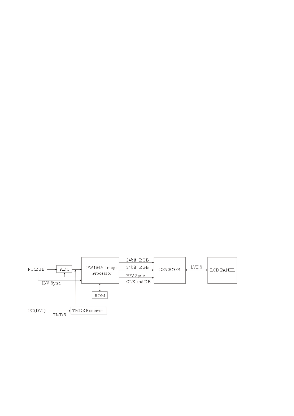
2. VL-706 DISPLAYCONTROL BOARD...............................................................9
A. Description .............................................................................................................................. 9
B. Features.................................................................................................................................. 9
C. BLOCK DIAGRAM.................................................................................................................. 9
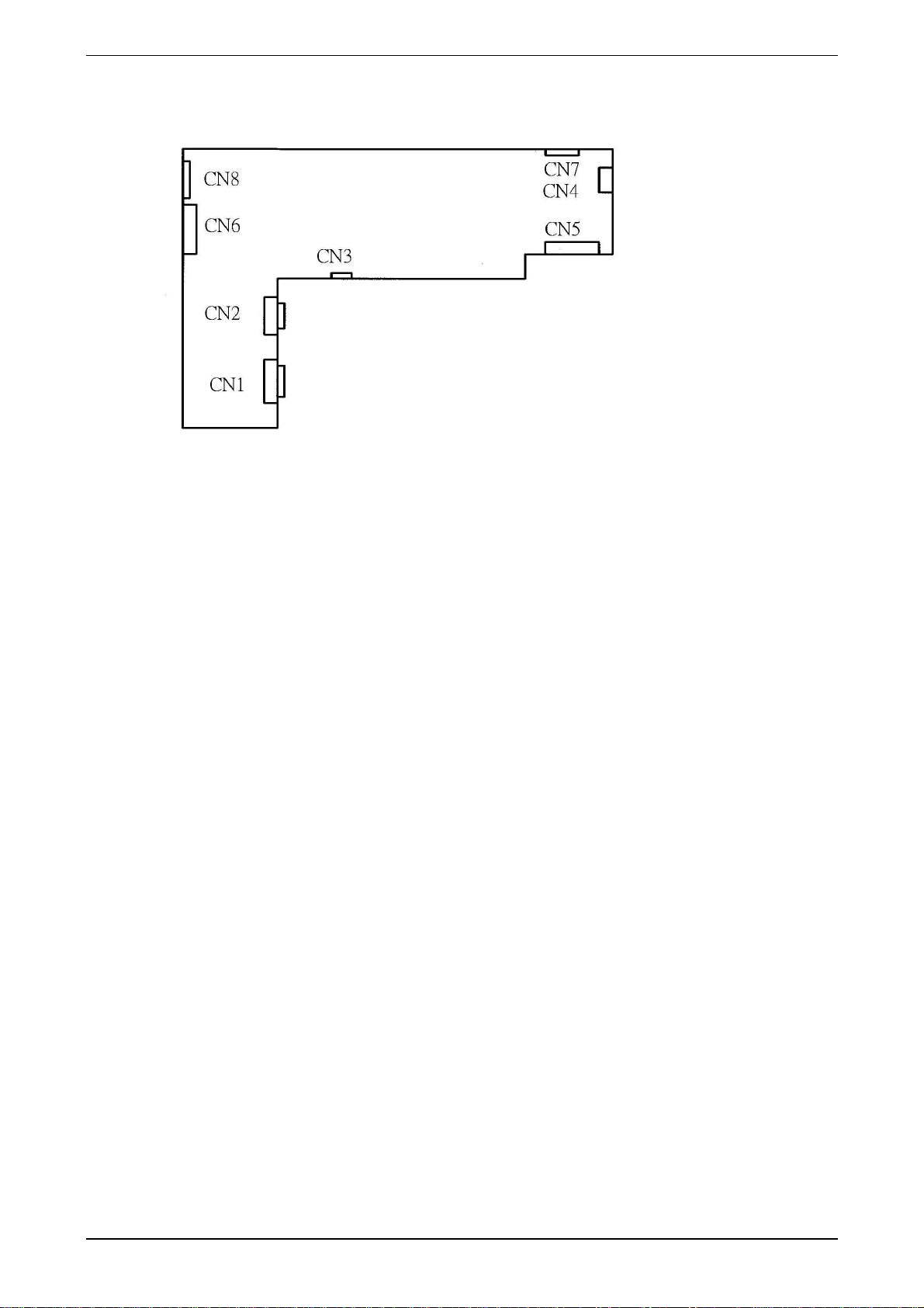
D. Connector Locations............................................................................................................... 10
E. Connector Type....................................................................................................................... 10
F. Connector pin assignment....................................................................................................... 10
3. VC-702 LVDS SIGNALTRANSFER BOARD.....................................................13
A. Description .............................................................................................................................. 13
B. Connector Locations ............................................................................................................... 13
C. Connector Type....................................................................................................................... 13
D. Connector pin assignment...................................................................................................... 13
4. VK-517 CONTROL PANEL ANDAUDIO BOARD.............................................14
A.Description ............................................................................................................................... 14
B.Connector and Switch Locations.............................................................................................. 14
C.Connector type......................................................................................................................... 14
D.Connector pin Assignment....................................................................................................... 14
5. VM-517 POWER ANDAUDIO............................................................................17
A. Major Specification.................................................................................................................. 17
B. Description .............................................................................................................................. 17
C. Efficiency:................................................................................................................................ 17
D. Connector Locations............................................................................................................... 17
E. Connector type........................................................................................................................ 17
F. Connector pin Assignment...................................................................................................... 18
6. ACADAPTER (LSL9901B12320)......................................................................19