HopeRF RFM380F64 User manual

434MHz SoC Wireless transceiver module
Product overview
The RFM380F64 is an integrated ARM Cortex-M0 32-bit CPU kernel with an
ultra-low-power RF transceiver, low-power consumption, high sensitivity, remote
communication, and a highly cost-effective SoC RF transceiver module.
Integrated with rich peripherals, support standard UART, I2C and SPI
interfaces, providing multiple general IO, support internal fast RC concussion,
internal slow RC concussion and 32.768 kHz external crystal oscillator, support
multiple package formats and codec, up to 64-byte Tx / Rx FIFO, feature-rich
RF GPIO, multiple low-power operating modes and fast start mechanism, high
precision RSSI, manual fast frequency hopping and multi-channel input 12-bit
high-speed ADC.
The product is divided into 434MHz working frequencies, supporting a
data rate range of 0.5-300kbps
RFM380F32
product features
Super anti-interference ability, suitable for the use of complex
interference environment scenarios
Receive sensitivity: -120 d B m @ 434MHz,0.6bps, GFSK
Operating frequency: 434MHz
Power supply voltage input range: 1.8V—3.6V
Emission current: 74mA @ + 20dBm, 434MHz
Receive current: 12mA @434MHz, FSK
Deep sleep current: 2.5uA
Operating rate: 0.5-300 kbps
applied range
Automatic meter reading
Furniture Security and Building automation
Wireless sensing nodes and industrial monitoring
ISM frequency band data communication

Product foot position
Figure 1: RFM380F32 Face View

Table 1, the foot-bit definition of the RFM380F32
foot
name
describe
Configuration function
1
P36
MCU and so on
IO
UART1_RXD、
TIM6_CHA、
UART0_RXD、
PCA_CH4、
TIM5_CHA、
spi_mosi、i2c_scl、AIN6/VC6/AVREF
2
P35
MCU and so on
IO
UART0_TXD,
TIM0_GATE、
TIM4_CHB、
SPI_MISO,
I2C_SDA,
AIN5/VC5,UART1 TXD
3
RESET
Hard reset pin
-------------------
4
P33
MCU and so on
IO
UART2_RXD、pca_ch1、tim5_chb、PCA_ECI、UART1_RXD、
XTL_OUT、TIM1_TOGN、AIN3/VC3
5
GPIO3
The GPIO3 of the
RF
CLKO, DOUT/DIN, INT2,DCLK (TX/RX)
6
VCC
Positive power
supply
---------------------
7
GND
earth wire
--------------------
8
RFOUT
RF output
---------------------
9
P01
MCU and so on
IO
UART0_RXD,I2C_SDA, UART1_TXD, TIM0_TOG, TIM5_CHB,
SPI_SCK, TIM2_EXT, AIN7/VC7,XTHI
10
P02
MCU and so on
IO
uart0_txd,i2c_scl,uart1_rxd,tim0_togn,tim6_cha,spi_cs,
tim2_gate,ain8,extho
11
P25
MCU and so on
IO
SPI_SCK、pca_ch0、tim5_cha、LVD_OUT、UART2_RXD、
I2C_SDA、TIM1_GATE、LVDIN3/VC1
12
P26
MCU and so on
IO
SPI_MOSI,TIM4_CHA,TIM5_CHB,PCA_CH2,UART2_TXD,
I2C_SCL,TIM1_EXT,AIN
13
SWDIO
SW shakedown
test IO
------
14
SWCLK
TheSW
debugging clock
--------
15
GPIO1
The GPIO1 of the
RF
DOUT/DIN, INT1,INT2,DCLK (TX/RX),RF_SWT
remarks:
1 RFM380F32 chip 32nd foot SCLK and chip 27th foot has been external connected
2 RFM380F32 chip 33rd foot SDA and the chip 26th foot are external connected
3 RFM380F32 chip 34th foot CSB and the chip 23th foot are external connected
4 RFM380F32 chip 35th foot FCSB and chip 9th foot has been external

Electrical parameters
Test conditions, power supply 3.3V, temperature 25℃
Table 2, a list of electrical parameters
parameter
symbol
status
least
value
representa
tive value
crest value
unit
service frequency
RFM380F32-433S2
434
MHZ
mode
MOD
FSK
receiving
sensitivity
434MHz1 Kbps
-120
DBM
data rate
DR
0.5
2.4
300
Kbps
Receive
bandwidth
BW
50
330
KHZ
working voltage
VDD
1.8
3.3
3.6
V
Receiveworking
current
IRX
434MHZ
9
10
mA
Launchworking
current
ITX
434MHZ +20dbm
70
80
mA
Sleep current
ISleep
1
uA
image rejection
IMR
33
dB
image rejection
Top
-40
+80
℃

Module outline dimension drawing
Figure 2, the module size diagram

FCC Statement
FCC standards: FCC CFR Title 47 Part 15 Subpart C Section 15.231
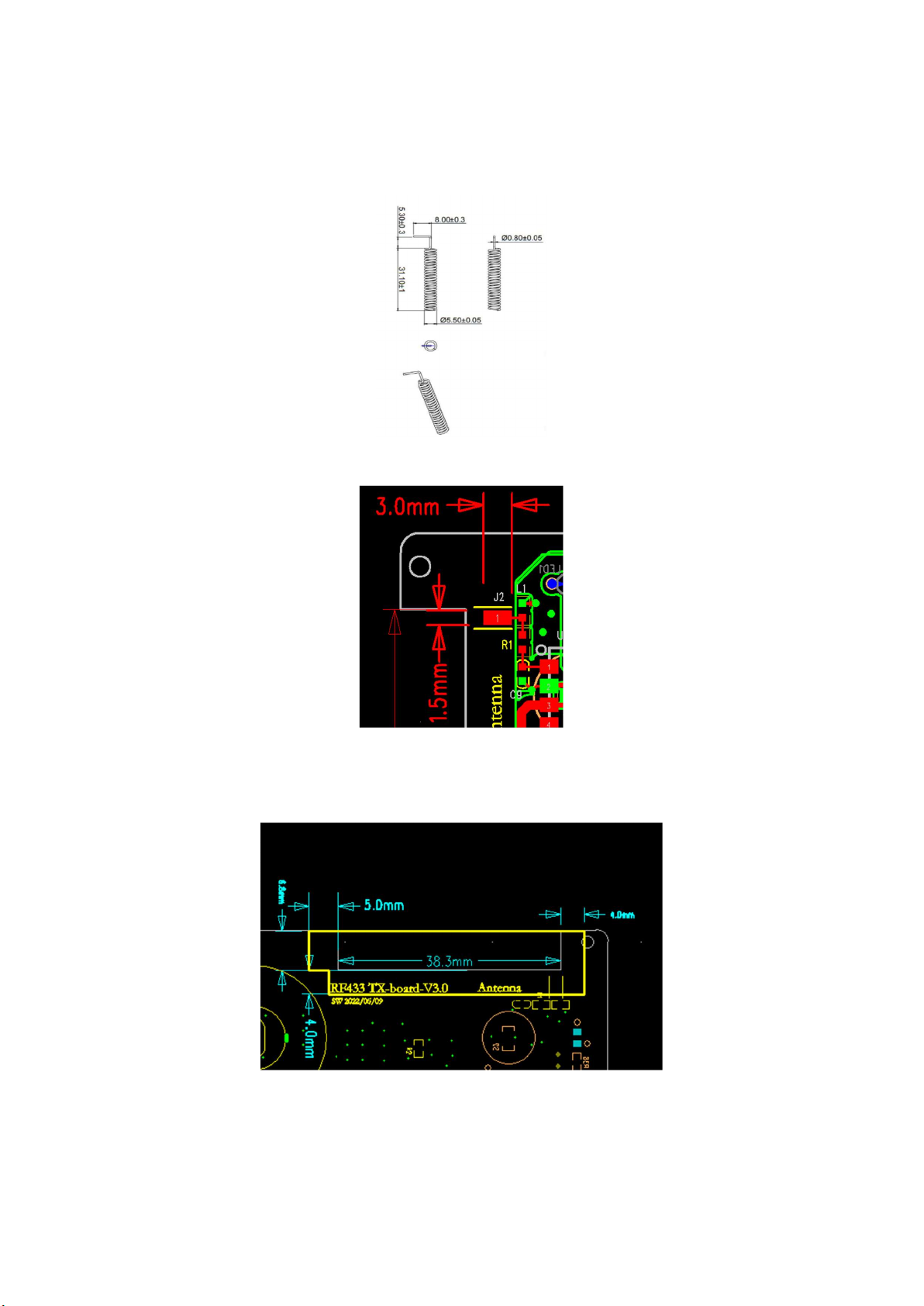
Trace antenna with antenna gain 3.555dBi
This device complies with part 15 of the FCC Rules. Operation is subject to the following two conditions:
(1) This device may not cause harmful interference, and (2) this device must accept any interference
received, including interference that may cause undesired operation.
Any Changes or modifications not expressly approved by the party responsible for compliance could void
the user's authority to operate the equipment.
Note: This equipment has been tested and found to comply with the limits for a Class B digital device,
pursuant to part 15 of the FCC Rules. These limits are designed to provide reasonable protection against
harmful interference in a residential installation. This equipment generates, uses and can radiate radio
frequency energy and, if not installed and used in accordance with the instructions, may cause harmful
interference to radio communications. However, there is no guarantee that interference will not occur in a
particular installation. If this equipment does cause harmful interference to radio or television reception,
which can be determined by turning the equipment off and on, the user is encouraged to try to correct the
interference by one or more of the following measures:
—Reorient or relocate the receiving antenna.
—Increase the separation between the equipment and receiver.
—Connect the equipment into an outlet on a circuit different from that to which the receiver is connected.
—Consult the dealer or an experienced radio/TV technician for help.
FCC Radiation Exposure Statement
This modular complies with FCC RF radiation exposure limits set forth for an uncontrolled environment.
This transmitter must not be co-located or operating in conjunction with any other antenna or transmitter.
If the FCC identification number is not visible when the module is installed inside another device, then the
outside of the device into which the module is installed must also display a label referring to the enclosed
module. This exterior label can use wording such as the following: “Contains Transmitter Module FCC ID:
2ASEORFM380F32 Or Contains FCC ID: 2ASEORFM380F32”
When the module is installed inside another device, the user manual of the host must contain below warning
statements;
1. This device complies with Part 15 of the FCC Rules. Operation is subject to the following two conditions:
(1) This device may not cause harmful interference.
(2) This device must accept any interference received, including interference that may cause undesired
operation.
Note: This equipment has been tested and found to comply with the limits for a Class B digital device,
pursuant to part 15 of the FCC Rules. These limits are designed to provide reasonable protection against
harmful interference in a residential installation. This equipment generates, uses and can radiate radio
frequency energy and, if not installed and used in accordance with the instructions, may cause harmful
interference to radio communications.
However, there is no guarantee that interference will not occur in a particular installation. If this equipment
does cause harmful interference to radio or television reception, which can be determined by turning the
equipment off and on, the user is encouraged to try to correct the interference by one or more of the
following measures:
—Reorient or relocate the receiving antenna.
—Increase the separation between the equipment and receiver.

—Connect the equipment into an outlet on a circuit different from that to which the receiver is connected.
—Consult the dealer or an experienced radio/TV technician for help.
2. Changes or modifications not expressly approved by the party responsible for compliance could void the
user's authority to operate the equipment.
The devices must be installed and used in strict accordance with the manufacturer's instructions as described
in the user documentation that comes with the product.
Any company of the host device which install this modular with modular approval should perform the test of
radiated & conducted emission and spurious emission,etc. according to FCC part 15C : 15.231 and 15.209 &
15.207 ,15B Class B requirement, Only if the test result comply with FCC part 15C : 15.231 and 15.209 &
15.207 ,15B Class B requirement,then the host can be sold legally.

Directional spring antenna specification
Below is ntenna specification
You can see antenna size from below specification
And PCB Pad size for spring antenna just follow the below chart.
Spring antenna location on PCB are J2, and the Empty Area except spring antenna should be see
just follow the below two charts.

L1——15nH,0603;
R1——0Ω,0603;
C9,no use
RF433
module
The RF line
This manual suits for next models
1
Table of contents
Other HopeRF Transceiver manuals
Popular Transceiver manuals by other brands

Crestron
Crestron CWD6660 Operation guide

Delta Electronics
Delta Electronics LCP-200A4HSR Specifications

Kenwood
Kenwood TM-261A instruction manual

Kenwood
Kenwood TM-401A instruction manual

Altronix
Altronix HubWay8D installation guide

Transition Networks
Transition Networks ETHERNET E-TBT-MC01(LC) user manual