Sect.
I1
Page 2
2) Set the
RANGE
and FREQUENCYcontrols for the
desired frequency. The frequency dial scale must
be
multiplied by
the
multiplying factor indicated by
the RANGE switch setting to obtain the oscillator
frequency. Example: 4 (on dial scale)
x
.l
(multi-
plying factor indicated by RANGE switch setting)
=
.4 cycles/sec.
3)
Set the FUNCTION switch for the desired output
waveform.
4)
Connect the equipment under test to the OUTPUT
terminals.
5) Adjust the AMPLITUDE Controlfor thedesired
output voltage. Because the frequency response
is
rated k0.2 db, the output amplitude may
be
mea-
sured
at
any convenient frequency and the output
level will be correct (within these limits) for any
other frequency.
must
be
connected
to
one of the OUTPUT terminals,
and the strappedpair will then be the ground side of
the output.
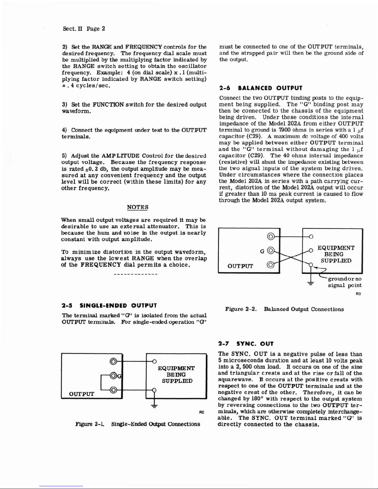
2-6
BALANCED
OUTPUT
Connect the two OUTPUT binding posts
to
the equip-
ment being supplied. The "G" binding post may
then
be
connected to the chassis of the equipment
being driven. Under these conditions the internal
impedance of the Model 202A from either OUTPUT
terminal to ground
is
7900 ohms in series with a 1pf
capacitor (C29). A maximum dc voltage of 400 volts
may
be
applied between either OUTPUT terminal
and the "G" terminal without damaging the 1 pf
capacitor (C29). The 40 ohms internal impedance
(resistive) will shunt the impedance existing between
the two signal inputs of the system being driven.
Under circumstances where the connection places
the Model 202A
in
serieswith a path carrying cur-
rent, distortion of the Model 202A output will occur
if
greater than 10 ma peak current
is
caused to flow
through the Model 202A output system.
NOTES
When small output voltages are required it may
be
To
minimize distortion in the output waveform, EQUIPMENT
always use the lowest RANGE when the overlap
of
the FREQUENCY dial permits
a
choice. SUPPLIED
-------------
groundorno
-
signal point
desirable to use
an
externalattenuator. This
is
2-5
SINGLE-ENDED
OUTPUT
Figure 2-2. Balanced Output Connections
The terminal
marked
"(3"
is
isolated from the actual
because the hum and noise
in
the output
is
nearly
constant with output amplitude.
OUTPVT terminals. For single-ended operation
"(3'
2-7
SYNC.
OUT
@
The SYNC. OUT
is
a negative pulse of less than
0
5 microseconds duration and
at
least 10 volts peak
EQUIPMENT into
a
2,500 ohm load.
It
occurs on one of the sine
BEING and triangular crests and atthe rise orfallof the
SUPPLIED squarewave.
It
occurs atthe positive crests with
respect to one of the OUTPUT terminals and at the
negative crestof the other. Therefore,
it
can
be
changed by 180" with respect
to
the output system
-
-
by reversing connections to the two OUTPUT ter-
RO
minals, which are otherwise completely interchange-
able. The SYNC. OUT terminal marked "G1'
is
FYgwe
2-L Single-Ended
Output
Co~ections directly connected to the chassis.
0