HP Compaq 370 User manual

TRADEMARK
All products and company names are trademarks or registered
trademarks of their respective holders.
These specifications are subject to change without notice.
Manual Revision 1.0
May 24, 2001
User’User’
User’User’
User’ss
ss
s
ManualManual
ManualManual
Manual
A SocA Soc
A SocA Soc
A Sockk
kk
ket 370 Pret 370 Pr
et 370 Pret 370 Pr
et 370 Processor basedocessor based
ocessor basedocessor based
ocessor based
mainboard (100/66 MHz)mainboard (100/66 MHz)
mainboard (100/66 MHz)
SupporSuppor
SupporSuppor
Supports PC100 Memorts PC100 Memor
ts PC100 Memorts PC100 Memor
ts PC100 Memory Modulesy Modules
y Modulesy Modules
y Modules
60002MC10
Get other manuals https://www.bkmanuals.com

Table of Contents
Section 1 Introduction
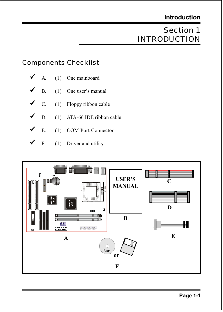
Components Checklist ........................................ 1-1
Form-Factor......................................................... 1-2
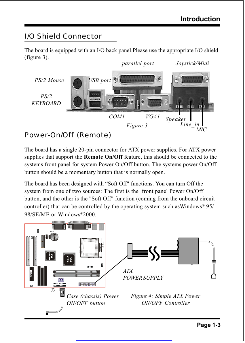
I/O hield Connector .......................................... 1-3
Power-On/Off (Remote) ..................................... 1-3
ystem Block Diagram........................................ 1-4
Section 2 Features
Mainboard Features ............................................. 2-1
Section 3 Installation
Mainboard Detailed Layout ................................. 3-2
Easy Installation Procedure
CPU Insertion ...................................................... 3-3
Jumper ettings ................................................... 3-5
ystem Memory Configuration .......................... 3-7
Device Connectors .............................................. 3-9
Section 4 Award BIOS Setup
BIO Instructions ................................................ 4-1
tandard CMO etup ......................................... 4-2
BIO Features etup ........................................... 4-3
Chipset Features etup ........................................ 4-8
Power Management etup ................................... 4-11
PNP/PCI Configuration ...................................... 4-14
Integrated Peripherals ......................................... 4-17
Load etup Defaults ............................................ 4-20
ensor and CPU peed etup .............................. 4-21
Change upervisor or User Password................. 4-23
Page
Get other manuals https://www.bkmanuals.com

IDE HDD Auto Detection..................................... 4-24
ave & Exit etup ................................................ 4-26
Exit Without aving ............................................. 4-26
Appendix
Appendix A
GHO T 5.1/6.03 Quick Users Guide ................ A-1
Appendix B
Update Your ystem BIO .................................. B-1
Get other manuals https://www.bkmanuals.com

Introduction
Page 1-1
Section 1
INTRODUCTION
Components Checklist
99
99
9A. (1) One mainboard
99
99
9B. (1) One users manual
99
99
9C. (1) Floppy ribbon cable
99
99
9D. (1) ATA-66 ID ribbon cable
99
99
9. (1) COM Port Connector
99
99
9F. (1) Driver and utility
USERS
MANUAL
B
A
C
D
F
or
E
Get other manuals https://www.bkmanuals.com

Introduction
Page 1-2
Mainboard Form Factor
The board is designed with MicroATX form factor - the new industry standard of
chassis. The MicroATX form factor is essentially a Baby-AT baseboard rotated 90
degrees within the chassis enclosure and a new mounting configuration for the
power supply. With these changes the processor is relocated away from the
expansion slots, allowing them all to hold full length add-in cards. MicroATX
defines a double height aperture to the rear of the chassis which can be used to
host a wide range of onboard I/O. Only the size and position of this aperture is
defined, allowing PC manufacturers to add new I/O features (e.g.; TV input, TV
output, joystick, modem, LAN, etc.) to systems. This will help systems integra-
tors differentiate their products in the marketplace, and better meet your needs.
Smaller size promotes a smaller system size.
I/O shield does not need to be retooled in an ATX 2.01 or later. Mainboard
could be used in an ATX 2.01-compliant.
A smaller power supply cam be used. High integration on mainboard reduces
the system costs.
PCI slots
Expandable I/O
5 1/4"
Bay
3 1/2"
Bay
Figure 2: Summary of Micro ATX chassis features
CPU located near
Power S pply
Single chassis
fan for
system
Micro
ATX
Power
Supply
ATX power
connector
Floppy / IDE
connectors
Get other manuals https://www.bkmanuals.com

Introduction
Page 1-3
Case (chassis) Power
ON/OFF utton
ATX
POWER SUPPLY
Figure 4: Simple ATX Power
ON/OFF Controller
Power-On/Off (Remote)
The board has a single 20-pin connector for ATX power supplies. For ATX power
supplies that support the Remote On/Off feature, this should be connected to the
systems front panel for system Power On/Off button. The systems power On/Off
button should be a momentary button that is normally open.
The board has been designed with Soft Off" functions. You can turn Off the
system from one of two sources: The first is the front panel Power On/Off
button, and the other is the "Soft Off" function (coming from the onboard circuit
controller) that can be controlled by the operating system such asWindows® 95/
98/S /M or Windows®2000.
I/O Shield Connector
The board is equipped with an I/O back panel.Please use the appropriate I/O shield
(figure 3).
J3
PS/2 Mouse
PS/2
KEYBOARD
COM1 VGA1
parallel port
Speaker
Joystick/Midi
USB port
Line_in
MIC
Figure 3
Get other manuals https://www.bkmanuals.com

.A=JKHAI
Page 2-1
Section 2
FEATURES
Mainboard Features:
PROCESSOR
- Socket 7 CPUs: Operating at 166-550MHz
- AMD K6- /III, Cyrix M II, Idt C6 / Winchip and Rise mP6 series
- Intel Pentium ®/Pentium ® Processor with MMXTM Technology,
CHIPSET
- VIA Apollo MVP4 AGPset (VT8501 + VT8 C686A)
DRAM MODULE
- 168pin DIMM x for PC100 Memory
- DRAM Size: 3 MB to 56MB
EXPANSION SLOT
- PCI x
- AMR Slot x 1
ONBOARD I/O
- On-Chip Multi I/O integrated with K/B, mouse, FDD, Parallel and Serial,
Fast IR and Power-ON controllers
ONBOARD PCI / IDE
- PCI Bus IDE Port with PIO /Ultra DMA-66x (Up to 4 Devices)
I/O CONNECTOR
- PS/ Mouse and PS/ style Keyboard
Get other manuals https://www.bkmanuals.com

.A=JKHAI
Page 2-2
USB
- USB connector x 4 ( for Opt.)
BIOS
- Award Plug & Play BIOS
Built-in AC9 Digital Audio (by VT82C686A)
- Dual full-duplex Direct Sound channels
- H/W Sound Blaster Pro for DOS legacy compatibility
- FM synthesis for legacy compatibility
- Supports game and MIDI port
Built-in Trident AGP Core
EXTENDED FUNCTION
- Supports exclusive USDM(Unified System Diagnostic Manager) and
Hardware Monitoring Function by VT8 C686A
- Supports exclusive KBPO(KeyBoard Power On)
- Supports CPU Clock setting via DIP Switch
- Supports Wake-On-LAN Function
FORM FACTOR
- 35mm x 180mm Micro ATX Size
Get other manuals https://www.bkmanuals.com

Installation
Page 3-2
Easy Installation Procedure
The following must be completed before powering on your new system:
3-1. CPU Insertion
3-2. Jumper Settings
3-3. System memory Configuration
3-4. Device Connectors
Section 3-1
CPU Insertion
CPU Insertion
Step 1
Open the socket by raising the actuation
lever.
Figure 2
Step 2
Insert the processor.
nsure proper pin 1 orientation by aligning
the FC-PGA corner marking with the
socket corner closest to the actuation arm
tip. The pin field is keyed to prevent mis-
oriented insertion.
Dont force processor into socket. If it does
not go in easily, check for mis-orientation and
debris. Make sure the processor is fully in-
serted into the socket on all sides.
Figure 3
Get other manuals https://www.bkmanuals.com

Installation
Page 3-3
Step 3
Close the socket by lowering and
locking the actuation lever.
Note: Intels reference design thermal solution is an active heatsink; an extruded alumi-
num heatsink based and a fan attached to the top on the fin array. ( ee Figure 5)
Figure 4
Figure 5
Get other manuals https://www.bkmanuals.com

Installation
Page 3-4
Section 3-2
Jumper Settings
SW1: CPU Speed Selection
1WS suB
kcolC
1234
NOzHM66
NOzHM57
NONOzHM38
NONOzHM09
NONOzHM59
NONONOzHM001
NONONOzHM501
NONONOzHM511
1WS UPC
reilpiluM
6CTDI/xiryC/DMA
UPC
reilpiluM
2pihCniWTDI
567
NOX2
NONOX5.2
NOX3
X5.3
NONOX4
NONONOX5.4
NONOX533.2
NOX5.566.2
JP2: CPU Vcore Voltage Selection
2PJerocVUPC
9-1V8.1
01-2V0.2
11-3V1.2
21-4V2.2
31-5V4.2
41-6V8.2
51-7V9.2
61-8V2.3
1
8
9
16
2.0V
1.8V
2.2V
2.1V
2.4V
2.8V
2.9V
3.2V
Get other manuals https://www.bkmanuals.com

Installation
Page 3-5
+276OFA 59 CPU
Bus
Clock
CPU
Multiplier
Pentium/MMX
AMD K6/K6-2/K6III
IDT-C6
Cyrix /IBM
6x86MX/MII IDT Winchip 2 Rise MP6 1234567
166MHz PR200 ON ON ON 66MHz
2.5X
PR233 ON ON ON 75MHz
PR266 233MHz ON ON ON ON 3MHz
PR300 *PR333 ON ON ON ON 95MHz
250MHz PR366 300MHz *PR366 ON ON ON ON ON 100MHz
200MHz PR266 200MHz ON ON 66MHz
3X
PR300 225MHz ON ON 75MHz
250MHz PR333 266Mhz ON ON ON 3MHz
PR400 *PR3 0 ON ON ON 95MHz
300MHz *PR433 *PR400 ON ON ON ON 100MHz
233MHz PR300 233MHz ON 66MHz
3.5X
PR333 ON 75MHz
*PR400 ON ON 3MHz
333MHz *PR466 *PR433 ON ON 95MHz
350MHz *PR500 *PR466 ON ON ON 100MHz
266MHz *PR333 266MHz ON ON ON 66MHz
4X
*PR400 ON ON ON 75MHz
333MHz *PR466 ON ON ON ON 3MHz
3 0MHz *PR533 ON ON ON ON 95MHz
400MHz *PR550 ON ON ON ON ON 100MHz
300MHz ON ON ON ON 66MHz 4.5X
450MHz ON ON ON ON ON ON 100MHz
333MHz ON ON ON 66MHz
5X475MHz ON ON ON ON 95MHz
*500MHz 266MHz ON ON ON ON ON 100MHz
366MHz ON ON 66MHz 5.5X
*550MHz 300MHz ON ON ON ON 100MHz
Get other manuals https://www.bkmanuals.com

Installation
Page 3-6
Section 3-3
System Memory Configuration
Memory Layout
The board supports (2) PC100 168-pin DIMMs (Dual In-line Memory Module).
The DIMMs is for SDRAM (Synchronous DRAM) .
DIMM SDRAM may be 83MHz (12ns), 100MHz (10ns),
125MHz (8ns) bus speed.
If you use both 50ns and 60ns memory you must configure
your BIOS to read 60ns.
When using Synchronous DRAM we recommend using the
4 clock variety over the 2 clock.
Figure 6 and Table 1 show several possible memory configuration.
* SDRAM supports 32, 64, 128, 256MB DIMM modules.
* e recommend to use PC100 Memory Module for bus speed between
66MHz and 100MHz.
* Using non-compliant memory with higher bus speed (over clocking) may
severely compromise the integrity of the system.
DIMM 1
DIMM 2
Bank 0/1
Bank 2/3 -Synchronous
DRAM
yromeMatoT 1MMID
)1/0knaB(
2MMID
)3/2knaB(
BM652=
mumixaM
*MARDS
,BM821,BM46,BM23
1XBM652
enoN
BM215=
mumixaM
*MARDS
,BM821,BM46,BM23
1XBM652
*MARDS
,BM821,BM46,BM23
1XBM652
Figure 6
Table 1
Get other manuals https://www.bkmanuals.com

Installation
Page 3-7
DIMM Module Installation
Figure 7 displays the notch marks and what they should look like on your DIMM
memory module.
DIMMs have 168-pins and two notches that will match with the onboard DIMM
socket. DIMM modules are installed by placing the chip firmly into the socket at a
90 degree angle and pressing straight down (figure 8) until it fits tightly into the
DIMM socket (figure 9).
Figure 7
Figure 9
DIMM Module clip after installation
To remove the DIMM module simply press down both of the white clips on
either side and the module will be released from the socket.
Figure 8
DIMM Module clip before installation
C NT R K Y ZON
(3.3 V DRAM)
L FT K Y ZON
(UNBUFFERED)
Get other manuals https://www.bkmanuals.com

Installation
Page 3-8
Section 3-4
Device Connectors
GND
PME
+5V Standby
J4
J6
J4/J6: CPU/Chassis Fan
A plug-in for the CPU/Chassis Fan Power
CPU Fan
J7: WOL (Wake On LAN) Connector
Reserved for NIC (Network Interface Card) to
wake the system.
GND
+12V
Rotation
PS/2 Mouse
PS/2
KEYBOARD
COM1 VGA1
parallel port
Speaker
Joystick/Midi
USB port
Line_in
MIC
Chassis Fan
GND
+12V
Rotation
Get other manuals https://www.bkmanuals.com

Installation
Page 3-9
FDD1: Floppy Controller Connector (Black color)
IDE1: Ultra ATA-66 Primary ID Connector
(White color)
IDE2: Ultra ATA-66 Secondary ID Connector
(White color)
PW1: ATX Power Connector
20-pin power connector
CD1: CD Audio_IN Connector
CD1
MODEM1
MODEM1: Telephony Connector for Modem audio
output
CD_IN_Left
1
CD_IN_Right
CD_Reference
CD_IN_Left
1
CD_IN_Right
GND
COM2
PW1
COM2: RS232 COM2 Connector
Get other manuals https://www.bkmanuals.com

Installation
Page 3-10
J3
Power On/Off
(This is connected to the power button on the
case. Using the Soft-Off by Pwr-BTTN feature,
you can choose either Instant Off (turns
system off immediately), or 4 sec delay (you
need to push the button down for 4 seconds
before the system turns off). When the system
is in 4 sec delay mode, suspend mode is
enabled by pushing the button momentarily.)
Turbo LED indicator
L D ON when higher speed is selected
IDE LED indicator
L D ON when Onboard PCI ID Hard disks is
activate
IR Connector
1. VCC 4. GND
2. NC 5. IRTX
3. IRRX
Power LED
Power L D connector
1. Power L D(+) 4. NC
2. N/C 5. GND
3. GND
Speaker
Connect to the system's speaker for beeping
1. Speaker 3. GND
2. N/C 4. GND
Reset
Closed to restart system.
J2
Get other manuals https://www.bkmanuals.com
Other HP Motherboard manuals
Popular Motherboard manuals by other brands

Fairchild
Fairchild FEB146-001 user guide

Linear Technology
Linear Technology DC512B quick start guide

Asus
Asus STRIX B250G GAMING quick start guide

Apex Digital
Apex Digital PA90 quick start guide

Avalue Technology
Avalue Technology RSC-IMX61 user manual

Texas Instruments
Texas Instruments ADS1 20EVM Series user guide