Hytera Transmitter User manual

Contents
Revision History.....................................................................................................................................0
Introduction ............................................................................................................................................1
Radio Controls........................................................................................................................................2
Circuit Description .................................................................................................................................3
Description of Components ................................................................................................................20
Tuning....................................................................................................................................................22
Port Definition.......................................................................................................................................22
Troubleshooting Flow Chart................................................................................................................26
Disassembly and Re-assembly for Repair.........................................................................................31
Exploded View......................................................................................................................................34
Packing..................................................................................................................................................36
MD78X PCB View..................................................................................................................................36
MD78X Block Diagram .........................................................................................................................36
Specifications.......................................................................................................................................37
Revision History
Material No. Date of
Issue
Changes
May 2010 Initial Release

1
Introduction
Manual Scope
This manual is intended for use by experienced technicians familiar with similar types of communication
equipment. It contains all service information required for the equipment and is current as of the
publication date.
This mobile radio shall be serviced by qualified technicians only.
Copyright Information
Hytera and HYT are the trademark or registered trademark of Hytera Communications Corporation
Limited (hereinafter referred to as “Hytera”) in PRC and other countries and/or areas. Hytera retains the
ownership of its trademarks and product names. All other trademarks and/or product names that may be
used in this manual are properties of their respective owners.
The Hytera product described in this manual may include Hytera computer programs stored in memory
or other media. Laws in the PRC and/or other countries or areas preserve for Hytera exclusive rights for
Hytera computer programs. The purchase of this product shall not be deemed to grant, either directly or
by implication, any rights to the purchaser with respect to Hytera computer programs. Any Hytera
computer programs may not be copied, modified, distributed, decompiled, or reverse-engineered in any
manner without the prior written consent of Hytera.
Disclaimer
Hytera endeavors to achieve the accuracy and completeness of this manual, but no warranty of
accuracy or reliability is given. All the specifications and designs are subject to change without prior
notice due to continuous technology development. Changes which may occur after publication are
highlighted by Revision History contained in Service Manual.
No part of this manual may be copied, modified, translated, or distributed in any manner without the
express written permission of Hytera.

2
Radio Controls
Front Panel
No. Part Name No. Part Name
○
1
Volume Control / Channel
Selector Knob
○
2 LED Indicator
○
3 LCD Display ○
4 OK/Menu Key
○
5 Back Key ○
6 Power On/Off Key
○
7 Up Key ○
8 Down Key
○
9 Speaker ○
10 Programmable Keys
○
11 Microphone Jack ○
12
Emergency key
(programmable)

3
Rear Panel
No. Part Name No. Part Name
○
1 Antenna Connector (BNC) ○
2 Power Inlet
○
3 Accessory Jack ○
4 GPS Antenna Connector
Circuit Description
1. Front Panel
The front panel provides parts including speaker, keys, power switch, volume control knob, LCD display
and etc. The block diagram is shown as the figure below:

4
Figure 1 Front Panel Block Diagram
1.1 Power Supply
The main board supplies power to the front panel via 5VD, so that RX/TX LED, backlight and USB
devices can be powered up. Power is further fed to U5 LDO, and then is supplied to LCD and
serial-to-parallel converter IC.
1.2 Keys
The front panel provides as much as ten keys including the programmable keys (S2, S3, S8, S9, S10
and S12), Up/Down key (S5, S11), Menu key (S4), Back key (S6), Power On/Off key (S1) and
Emergency key (S7).
A 3 row by 4 column matrix keyboard of the processor is used to identify operations of front panel keys.
Each of the 3 row signal lines are connected with the pull-up resistors R488, R499 and R511, and the 4
column lines are monitored to detect if a button has been pressed.
1.3 LCD Display
The TFT LCD can transfer data via the bus EMIFS of U302. Control signals include, write/read enable,

5
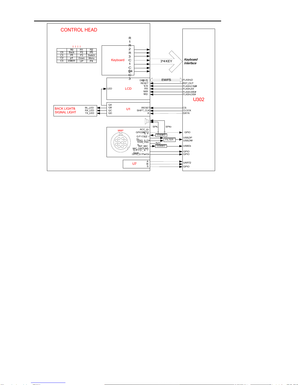
memory chip select, LCD chip select and reset signal, and the signals will be pulled up by R36, R35, R34,
R33 and R6 respectively. 5V voltage is converted to 3.3V by U5, and is then supplied to the LCD.
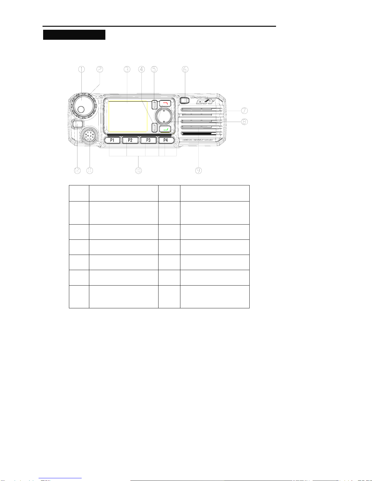
1.4 LED and Backlight
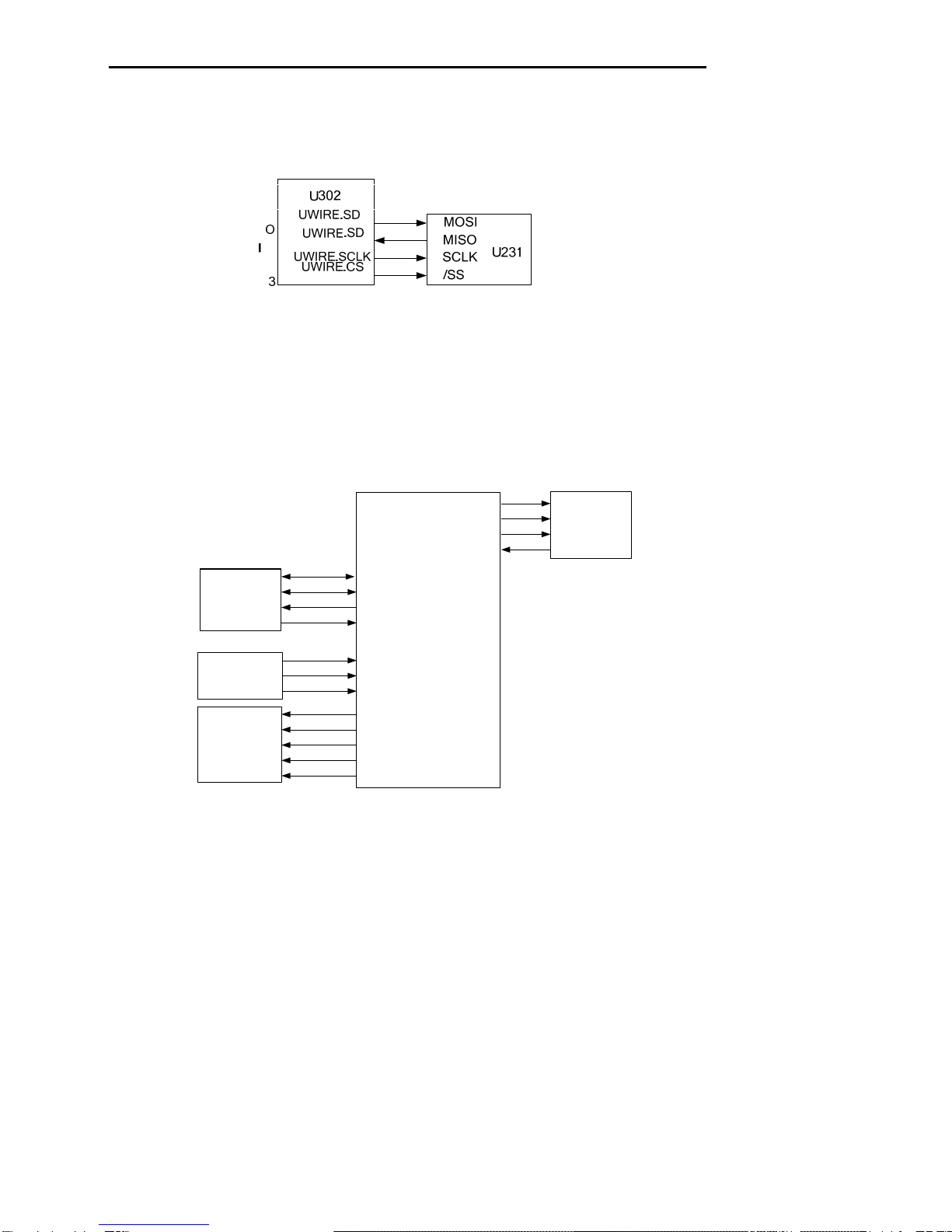
LED enable signal is fed to the serial-to-parallel converter IC, and then is output by U302. RX status is
indicated by green LED, and TX is by red LED. Backlight will be illuminated once any key is pressed.
The red and green LEDs in series are powered by 5V (U902) and controlled by Q2 and Q3. The
backlight is powered by 5V and controlled by Q1. Control signals are output via U1.
1.5 MMP Interfaces
The MMP interfaces are defined as follows:
No. Definition & Description
1 Accessory identifier
port 1
The pin together with pin 10 can form an accessory
identification matrix.
2 PTT input Used to input PTT signal from microphone. The pin is at
low level when PTT is hold down.
3 Handset audio
output
Used to output audio received from accessories; the
Handset option must be checked in the CPS.
4 USB_D- USB data line D-
5 GND Ground
6 USB_VBUS Provides +5V for USB accessories.
7 Mic input Used to input external microphone signal. Vrms=80mV
@ 3K dev.
8 USB_D+ USB data +
9 HOOK Valid upon low level. The default is high level.
MMP10
10 Accessory identifier
port 2
The pin together with pin 1 can form an accessory
identification matrix, details of which are stated in the file
“Definition of External Interfaces”.
Table 1 Definition of MMP Interfaces
1.6 Audio output
The front panel provides two paths of audio output Handset_audio and SPK±. Handset_audio is the
output of received audio via MMP interface, and SPK± is the output by the PA U201 as audio signal for
the front panel speaker.
1.7 Volume Control
The encoder switch U7 will generate volume adjustment signals, which will be routed to U302 by
GPIO17 and GPIO18.

6
2. Working Principle of Baseband
Power System
Figure 2 Diagram of Power Distribution
Both the baseband control IC and the RF section can convert the supplied voltage to the appropriate
level via the voltage conversion IC.
zRF section: U914, Q920 and Q921 supply power for the RF section. High current PNP transistor
and comparator can function as LDO (Low Dropout Regulator).
zFGU: U918 and U915 supply 3.3V and 5V respectively to U100.
zBaseband: the processor U302 is supplied by 3.3V (U900), 1.8V (U903) and 1.6V (U919); the
memories are supplied by 3.3V (U900) and 1.8V (U903) respectively; the audio processor IC is
supplied by 3.3V (U900&U909) and 1.8V (U903); the DAC is supplied by 5V (U905) and 3.3V
(U900).
zEXT_SWB+: Q909.
2.1 Power On/Off

7
The mobile radio can be powered on/off through any of the following methods:
1) Power On/Off key
2) Ignition sense or Power On/Off key
3) Emergency
2.1.1 Power On/Off key
After the user presses the front panel Power On/Off key, R944 is grounded, and Q910 and Q905 are
turned on, causing the power management IC U902 and Q920 to start working. Then the processor
U302 will execute user routines, and can identify power on/off signals if low level is detected from Q914,
using the level PWR_CTRL to maintain or cut off the connection with the power system.
2.1.2 Ignition Signal
When voltage of ignition signal exceeds 7V, Q1 will be turned on through charging by C933, R955 and
R956, and the PNP transistor of Q905 will be further turned on to supply power. Q401 will also be turned
on. If signal is detected from Q401, U302 can identify ignition signals and then will generate the level
PWR_CTRL.
2.1.3 Emergency Alarm
When the emergency alarm pin is at low level, R940 is grounded, and Q906 is turned on to supply power.
Q908 is also turned on. When low level is detected from Q908 but the radio is powered off, U302 will
output the level PWR_CTRL and send emergency signal. If the radio is powered on then, U302 will only
output emergency signal.
2.1.4 Power-up Process
1) Turn on the radio through any of the methods mentioned above, and ensure enough time for
U900, U902, U903 and U919 to be turned on.
2) U917 will generate reset signal and remain low level for 1.25 seconds. Then the processor
starts to work.
3) Each method will generate and send a specific power-up signal to the processor.
4) After the signal is received, the processor will generate the level PWR_CTRL, and finish
power-up procedures.
2.2 Clock

8
Figure 3 Diagram of Clock Distribution
2.2.1 Input Clock
32K clock is used for timing and sleep of the whole system. Frequency of this clock is 32.768kHz, which
is subject to frequency division without error by U302 to finally get 1Hz, usually used for counting
seconds. Frequency of system clock is 19.2MHz, generated by external crystal oscillator.
2.2.2 Output Clock
The baseband outputs 3 clock signals fed to U231, U100 and Option board respectively.
2.3 Interface Distribution
2.3.1 SPI Interface
Figure 4 SPI Interface Block Diagram
SPI interface of the processor U302 can operate in master mode, controlled by MPU or DMA. In master
mode, U302 can provide 4 chip select signals, with CS2 used to enable IF processor U701. In master
mode, the maximum data transfer rate is as high as system clock frequency.
2.3.2 MCSI Interface
U302 U100
Dat
a
CLK
MCSI1.CLK
MCSI1.DOUT
MSCI1.SYNC /CS
Figure 5 MCSI Interface Block Diagram
During communication between U302 and U100, the former works in master mode with clock frequency

9
of up to 9.6MHz, and the latter uses MCSI frame synchronization as chip select signal. MCSI1.DOUT as
a data line is used to configure the memory U100.
2.3.3 MICROWIRE Interface
Figure 6 MICROWIRE Interface Block Diagram
The MICROWIRE interface can accommodate 4 external devices at most, and is generally used for
receiving control and status messages from external devices, and can also be used for reading data
from ROM. Its maximum clock frequency is a quarter of system clock frequency. MICROWIRE is used
for configuration of and reading from the audio processor, and requires chip select signal CS3.
2.3.4 SSI Interface
MCBSP1.CLKX
MCBSP1.FSX
MCBSP1.DX
MCBSP1.DR
MCBSP3.CLKX
MCBSP3.FSX
MCBSP3.DX
MCBSP3.DR
U302
MCBSP2.CLKR
MCBSP2.FS
R
MCBSP2.DR
MCBSP2.CLKX
MCBSP2.FSX
MCBSP2.DX
GPIO29
GPIO31
BCLK
WCLK
U231
SDIN
SDOUT
PCMCLK
PCMSYNC
PCMIN
Option
Board
PCMOUT
CLKOUT
U701 FS
DOUTA
SCLK
U500
FS
DIN
/ LOAD
/PD
Figure 7 SSI Interface Block Diagram
U302 provides 3 McBSP interfaces McBSP1, McBSP2 and McBSP3, compatible with a variety of
interfaces. McBSP1 is connected with interface I2C of audio processor, to realize two-way transmission
of digital voice and data. McBSP2 uses independent clock and frame synchronization for transmitting
and receiving. Interface SSI of the receiver processor is connected with RX end of McBSP2, and U500 is

10
connected with TX end of McBSP2. U302 works in master mode. McBSP3 is connected to the Option
Board interface for both voice and data transmission.
2.3.4 USB Interface
Figure 8 USB Interface Block Diagram
The radio has two USB interfaces, and both are connected to the USB signal port of the processor. REF
CLOCK is the reference frequency in specified mode. It should be 12MHz in high rate mode or 1.5MHz
in low rate mode.
2.3.5 UART Interface
Figure 9 UART Interface Block Diagram
U302 provides three UART interfaces, which enables the processor to communicate with a variety of
external devices. UART2 is used for communication with front panel and serial port on PC, and UART3
is used for communication with Option board and accessory jack (USB).
2.3.6 Further Development Port (MAP)
Further development port includes audio interface, programmable I/O, serial port, USB port, accessory
identifier port and etc, used for further development by the user. The pins are defined as follows:
Pin Function Description

11
1 Vbus USB power supply +5V power supply
2 Ground
3 GP5_3 general purpose I/O port
(Chan_Act)
General purpose I/O port with function defined
through the CPS
4 SW B+ sense power output 13V output voltage; output current ≤1.5A
5 External Alarm Programmable output pin (the default is External
Alarm)
6 Power Ground
7 Tx Audio input (audio from external
mic)
Used to input signal from external mic; audio
path is valid upon press of external PTT.
8 RX Audio output Used to output received audio signal.
9 Spkr- External speaker output -
10 USB D+ USB data +
11 USB_GROUDN Ground line
12 GP5_2 general purpose I/O port
(Monitor)
General purpose I/O port with function defined
through the CPS (the default is Monitor)
13 ACC_IO2 Accessory identifier port; three kinds of
accessory identification status, and one default
status are provided by the pin together with pin
15 ACC_IO3.
14 Emergency switch When Emergency is active, this pin is at low
level.
15 ACC_IO3 Accessory identifier port
16 PRGM_IN_PTT Programmable input pin (the default is PTT)
valid upon low level
17 Audio Ground
18 Speaker + External speaker output +
19 USB D- USB data -
20 GP5_8 general purpose I/O port / serial
port RX general purpose I/O interface
21 Ground
22 GP5_7 general purpose I/O interface /
serial port TX general purpose I/O interface
23 GP5_6 general purpose I/O interface General purpose I/O interface with function
defined through the CPS
24 AUX Audio Output 1 External speaker audio output 1
25 AUX Audio Output 2 External speaker audio output 2
26 Ignition sense Used to input ignition voltage
Table 2 Definition of Further Development Port
2.4 Audio Path

12
INT_MIC
EXT_SPK
PUB_ADDRESS1
PUB_ADDRESS2
RX_AUDIO
Figure 10 Block Diagram of Audio Path Connection
2.4.1 RX Audio Path
U302 sends digital audio to the audio processor codec via the SSI bus of interface MCBSP1. The bus is
composed of CLKX, FSX, DX and DR. It sends the demodulated PCM audio signal to codec, and adjusts
the signal to appropriate amplitude according to the volume (RMS should be 80mv when frequency is 1k
and deviation is 3k). Then the codec converts PCM data into analog audio data via DAC. U231 provides
two outputs SPK1 and SPK2. SPK1 is amplified by U238 and then is fed to the PA U201, to derive two
outputs of received audio, which will be applied to the front panel speaker and further development
interface respectively. SPK2 is amplified and divided into the four paths of signal HANDSET_AUDIO,
RX_AUDIO, PUB_ADDESS1 and PUB_ADDESS2. The first two paths are amplified by U235, and the
last two paths are amplified by U236. Output of HANDSET_AUDIO, PUB_ADDESS1 and
PUB_ADDESS2 are controlled by Q231, Q235 and Q233 respectively.
2.4.2 TX Audio Path
There are two mic inputs applied to the audio processor U231. The internal mic is connected to the
interface MICIN_HND of U231, and is combined with AUX1 to provide differential input. After 9.3V is
divided by R255 and R264, a bias voltage of about 7V is provided to the front panel mic. The external
mic is connected to the interface MIC_HED of codec, featured as single-ended input . Q232 controls
switch between both mics. When internal mic is active, EXT_MIC_EN is at low level, bias voltage of
external mic is disconnected, and the ADC in U231 senses voltage at pin MICIN_HND. When external

13
mic is active, EXT_MIC_EN is at high level, Q232 is turned on, bias voltage is connected, and the ADC
in U231 senses only audio data at pin MICIN_HED.
Audio signals input from MMP interface or the accessory jack, are fed to the codec (gain of codec is
programmable via the CPS) and then are converted by the ADC into 16-bit PCM digital audio, which will
be fed to U302 via the interface SSI.
When the radio is set to operate in loudspeaker mode, audio signal is generated by the internal mic, and
then is fed to U231, and finally is output via SPK2. The output audio signal is amplified, and then is
output as the two paths of audio PUB_ADDRESS1 and PUB_ADDRESS2.
3. Working Principle of RF Section
3.1 UHF1 (400-470 MHz) Transmitter Circuit (5W-45W)
The transmitter section includes power amplifier circuit and power control circuit. The PA circuit is used
for signal amplification, so as to amplify VCO signal to the required output power level. The power
control circuit is used to maintain output power at the required level, and to protect the PA from heating,
and protect the driver PA Q801 (RD07MUS2B), pre-driver PA Q805 (RD01MUS1) and final PA
(PD85035S-E) from damage caused by antenna mismatch, or high/low voltage.
Figure 11 Block Diagram of Transmitter
3.1.1 Power Amplifier
The power amplifier comprises of four-stage amplifier circuits, to amplify VCO signal to the required
output power level. The first is the buffer amplifier circuit (BFG540W) with fixed gain, the second is the
pre-driver power amplifier circuit LDMOS (Lateral Double Diffuse MOS) (RD01MUS1) with variable gain,
the third is the driver power amplifier circuit LDMOS (RD01MVS1) with variable gain, and the last is the
final power amplifier circuit LDMOS (PD85035STR1-E) with fixed gain. The TX power amplifier circuit

14
also includes TX/RX switch and low pass filter.
3.1.2 TX Buffer Amplifier
The buffer amplifier BFG540W (Q801) provides about 16dB power gain, and adjusts the bias circuit to
get quiescent bias current of 28mA for Q801. Power supply for the switching transistor Q810 is
controlled by TX signal (antenna switch enable signal), so as to connect or cut off the power supply for
the whole circuit.
3.1.3 Pre-driver Power Amplifier
The pre-driver power amplifier comprises of LDMOS RD01MUS1 (Q805), with gain controlled by voltage
VGG. The input matching circuit is composed of C826, L826, L814, C843 and R824.
3.1.4 Driver Power Amplifier
The driver power amplifier comprises of LDMOS RD07MVS1 (Q804), with gain controlled by voltage
VGG. The maximum output power is 38.5dBm, and the maximum gain is above 11dB.
3.1.5 Final Power Amplifier
The final power amplifier comprises of two LDMOS PD85035STR1-E (Q802 and Q803), with the
maximum output power of 48.5dBm, and the maximum gain of above 10dB. The input matching circuit is
composed of C815, C839, R804, R806, R807, R813, R818 and R861. And the power combining circuit
comprises of C820, C8330, C831, C819, C812, C841 and C842.
3.1.6 Antenna Switch
The antenna switch is used to switch between the transmitter circuit and the receiver circuit. In TX mode,
the switching transistor Q810 is controlled by TX signal, so as to supply 9V 3A to the PIN diodes D801
and D802. Quiescent bias current of the PIN diode is controlled by the resistors R821 and R825. In TX
mode, D801 and D802 are turned on, and RF signals are applied to the low pass filter (C871, C816,
C836, C837, C838, L809, L813, and L810) and then transmitted via the antenna port.
In RX mode, TX signal controls the switching transistor Q810, to further control the power supply for the
PIN diodes D801 and D802, which has no DC bias current. When the two diodes are turned off, signals
are fed into the low pass filter (L871, C852, C862) and then passed to the RX path.
3.1.7 Low Pass Filter
The low pass filter comprises of inductors L809, L813 and L810, and capacitors C836, C837, C830 and
C838, and is used for attenuation of harmonic energy from the transmitter.
3.1.8 Directional Coupler
The directional coupler is comprised of the Microstrip Directional Coupler, D803, D804 and etc, and is

15
used for detecting forward power and reverse power of the transmitter. The forward power is coupled
with the diode D803, and the voltage is applied to the power control circuit (U801). Then the output
voltage VGG is applied to control the gate voltage of pre-driver and driver PA, for the purpose of stable
power output.
The directional coupler is not only the TX power adjustment circuit, but also a part of the VSWR
detection circuit. The reverse power is coupled with D804. The voltage is applied to U802 and then is fed
into U302 for judgment.
3.1.9 Output Power Control
The TX power is controlled via the power control IC U801. The forward power is applied to the directional
coupler, to output a voltage that can represent the forward power. The voltage together with the preset
voltage are fed into U801 to output a voltage VGG, which can control both gate voltage and gain of Q804
and Q805, for the purpose of stable power output.
3.1.10 Heating and Over-voltage Protections
The circuit comprises of thermistor RT804 and resistor R884. The output voltage is proportional to the
detected temperature. Both the voltage used for temperature detection and the threshold voltage are fed
into the operational amplifier U803, to output a voltage signal that is in proportional to the detected
temperature. The voltage is applied to software judgment, and then the preset voltage will be
subsequently changed to lower TX power, and to protect the PA from over-heating.
3.1.11 Pressure Pad Switch
The power control circuit includes a pressure pad switch SW1, which is controlled by the conductive
rubber part mounted on the top cover. When the switch is off, the power control voltage VGG is pulled
low, and the PA gives no power output. When the top cover is secured to the base, the switch will be
turned on and the PA will work normally. This mechanism will help to protect the PA from damage due to
improper installation.
3.2 UHF1 (400-470 MHz) Receiver Circuit
The receiver utilizes double conversion superheterodyne techniques. The first IF is 73.35MHz and the
second IF is 2.25MHz. The first local oscillator signal is supplied by the PLL circuit U100. And the second
local oscillator signal (71.1MHz) is generated by the PLL circuit U701. The main units are BPF and LNA,
mixer, IF filter, IF amplifier and IF processor.

16
Figure 12 Block Diagram of Receiver
3.2.1 Front-end Circuit
RF signals are fed into the low pass filter to remove signals above 550MHz, and are applied to the
two-stage band pass filter to select the wanted signal. TV can realize 400-470M bandwidth adjustment.
After passing through the BPF and LNA (Q6102), the RF signals together with the first local oscillator
signal are fed into the mixer for the first time frequency conversion, to generate the first IF signal
(73.35MHz). The passive diode mixer provides good dynamic range and port isolation. The local
oscillator signal (3-5dBm) supplied by the VCO is fed into Q6103, to get the required gain of 17dB. The
first local oscillator signal (73.35MHz) is applied to the crystal filter (Z6100) to remove out-of-band
spurious signal, and then is fed into the two-stage IF amplifier circuit composed of Q6133 and Q6134,
and finally goes to the IF processor AD9864.
3.2.1 Rear-end Circuit
16.8MHZ
Reference
frequency
IF input
SSI TO OMAP
Figure 13 IF processor AD9864
The IF signal (73.35MHz) goes into AD9864 via pin 47 for the second time mixing, to generate the
second IF signal (2.25MHz). Digital I/Q signal output from the SSI pin is fed into U302 (OMAP5912) to be
demodulated. AD9864 employs reference frequency of 19.2MHz and shares the crystal with OMAP. The

17
second local oscillator VCO comprises of external transistor, varactor and some other components, to
generate the second local oscillator signal. The 18MHz clock frequency is generated by LC resonance
loop (D702, L715, C745).
The 16-bit 20K audio signal output from AD9864 (U701) is applied to the DSP pin (U302C), and then is
applied to U302 to output 8K data signal, which will be fed into TLV320AIC29IRGZR (U231) and PIN44
(SSI_DI) for DAC. The output analog audio signal will be subject to gain control, and then will be output
to the speaker.
3.3 FGU
3.3.1 PLL Circuit
The PLL circuit is used to supply excitation signal source for the transmitter, and to supply local oscillator
signal for the receiver. It is composed of the reference crystal (X100), PLL IC (U100) and VCO.
3.3.2 Reference Crystal
X100 is a 19.2MHz TCXO, with frequency calibrated by the Digital to Analog (D/A) converter (U500).
3.3.3 PLL
The PLL IC (U100) is a fractional frequency divider. The logic IC U101 (MC74VHCS) and U102
(MC74VHCS) will work with the PLL IC to lock phase.

18
Figure 14 Block Diagram of PLL IC (U100)
The 19.2MHz frequency generated by the reference crystal (X100) is fed into the PLL IC (U100), to
generate the reference frequency. Frequency obtained from the PLL IC (U100) is fed into the phase
comparator, and is then converted to DC CV voltage via the loop filter, to control and lock the frequency.
3.3.4 VCO
VCO is comprised of transistors (Q100, Q103, Q106, Q110), varactors and four Colpitts Oscillators, with
two transistors (Q100 and Q103) as the source of excitation signal for TX, and the other two (Q106 and
Q110) as the source of local oscillator signal for RX. U302 controls the operating frequency of the VCO.
Q102 and Q107 constitute the buffer amplifier for the transmitter section, and Q111 and Q109 constitute
the buffer amplifier for the receiver section. The Digital to Analog (D/A) converter (U500) outputs
demodulation signal to demodulate TX oscillator signal.

19
PLL IC (U100)
Q103
LPF
Q110
Q100
Q106
Q102
Q111
Q107
MOD
RX_H_VCO
RX_L_VCO
TX_H_VCO
TX_L_VCO
Q109
TX PA
RX Lo
Figure 15 Block Diagram of VCO
System Test Plan
To help you test every unit circuits, we have designed test points on the key parts of the circuit. Test of
RF circuit is planned as follows:
1. PLL/VCO Section
Test
Points
Definition
TP101 Feedback signal output from VCO
TP102 RF signal output from VCO
TP103 CV voltage/LPF output
TP104 Modulation signal MOD1 output from DAC
TP105 Control voltage terminal of crystal
TP106 Modulation signal MOD2
TP107 PLL-Data
TP108 PLL-CLK
TP109 PLL-LE
TP110 LD detection signal
TP111 3.3VA
TP112 5V charge pump
Table 3 PLL/VCO Test Plan
2. TX/RX Circuit
Test
Points
Definition
TP601 9.3VA
Table of contents