Infineon XENSIV TLI4971 Operating instructions

Application Note Please read the Important Notice and Warnings at the end of this document Rev. 1.30
www.infineon.com page 1 of 31 2022-03-01
AppNote_TLI4971_ProgGuide
Current Sensor TLI4971
Programming Guide and User Manual
About this document
This document describes how to program the TLI4971 with the Infineon proprietary one wire interface (SICI).
Timing of the serial inspection interface.
Command structure and commands for write/read and EEPROM access.
A description of the user changeable EEPROM section.
Details on the diagnosis mode.
For productive in circuit programming Infineon recommends to use a verified programmer which has been a
coproduction development between Infineon and CGS. For further documentation please refer to Sensor –
Programmer –CGS –Computer Gesteuerte Systeme GmbH (cgs-gruppe.de)
Further Infineon provides a programming board for laboratory usage.
Scope and purpose
TLI4971 Coreless Current Sensor Feature set, EEPROM and interface description.
Intended audience
Users who use the high variety of the TLI4971 current sensor by programming the functionality like full scale
or over current detection, operating modes etc. to their need.
Current Sensor Module Developers.

Application Note 2 of 31 Rev. 1.30
2022-03-01
Current Sensor TLI4971
Programming Guide and User Manual
Current Sensor TLI4971
Table of contents
Current Sensor TLI4971 ................................................................................................................... 1
About this document....................................................................................................................... 1
Table of contents............................................................................................................................ 2
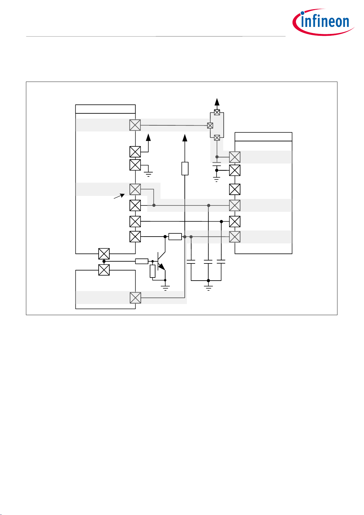
1Application and Programming circuit ....................................................................................... 3
1.1 Circuit / Precondition..............................................................................................................................3
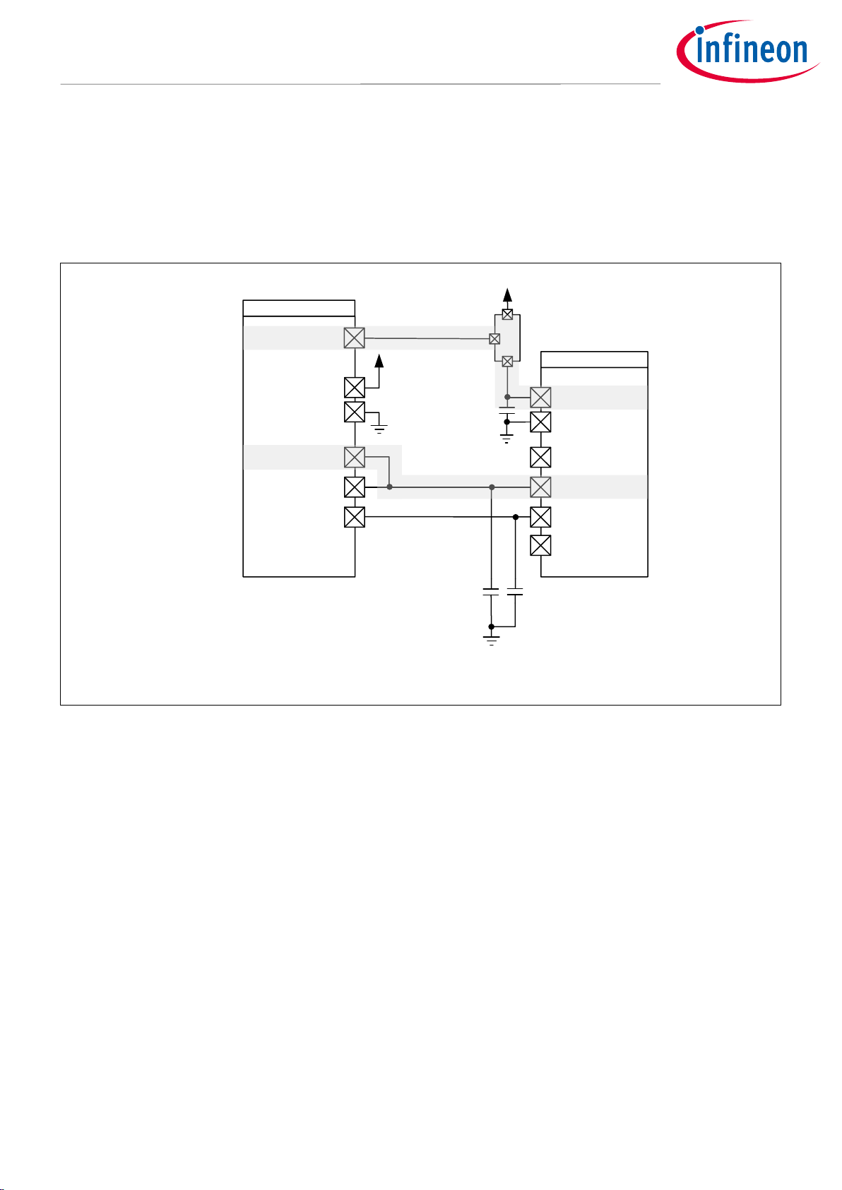
1.2 In-circuit programming...........................................................................................................................4
2Serial Inspection and Configuration Interface (SICI)................................................................... 6
2.1 Hardware Implementation .....................................................................................................................6
2.2 Entering Communication Mode..............................................................................................................6
2.3 Communication timing...........................................................................................................................7
2.3.1 Single low/high PWM transmission ...................................................................................................7
2.4 Interface Timing Definition.....................................................................................................................9
2.5 Definition of Voltage Levels ....................................................................................................................9
3Interface description .............................................................................................................10
3.1 Command Structure..............................................................................................................................10
3.2 Read / Write Command.........................................................................................................................10
3.3 Interface Commands.............................................................................................................................11
3.4 Write and programming sequence.......................................................................................................12
3.5 Temporary register................................................................................................................................12
3.6 Read Example (temperature register read out) ...................................................................................13
4EEPROM ...............................................................................................................................14
4.1 EEPROM Content...................................................................................................................................15
4.2 Programming Example .........................................................................................................................17
4.3 Margin Test ............................................................................................................................................19
4.4 Cyclic Redundancy Check .....................................................................................................................21
4.5 Code example CRC calculation.............................................................................................................23
5Operation Mode ....................................................................................................................24
5.1 Single-Ended Mode ...............................................................................................................................24
5.2 Fully-differential Mode..........................................................................................................................24
5.3 Semi-differential Mode..........................................................................................................................25
6How to connect the sensor in a 5V domain................................................................................26
6.1 Single-Ended Mode ...............................................................................................................................26
6.2 Semi and or Fully-differential Mode .....................................................................................................26
7Diagnosis Mode.....................................................................................................................27
8Glossary...............................................................................................................................29

Application Note 3 of 31 Rev. 1.30
2022-03-01
Current Sensor TLI4971
Programming Guide and User Manual
1Application and Programming circuit
The sensor has implemented a serial interface to set the EEPROM content. This chapter describes the hardware
environment to program the device. Further, it shows the recommended circuit for a three-phase GPD
application.
R3 4k7
AOUT
OCD2
VDD
GND
VDC_Link
PGND
VAREF
A/D
A/D
A/D
A/D
EN
VCC_IO
6
Gate-
Driver
µC
Load
VREF
OCD1
VCC_IO
IP+IP-
VCC_IO
220nF
4k7
1nF/50V
TLI4971
A/D
A/D
4k7
1nF/50V
GPIO
VAREF
PWM
AGND
AGND
GPIO
6.8nF/50V 6.8nF/50V 6.8nF/50V 6.8nF/50V 6.8nF/50V6.8nF/50V
R1 R2
C1
C2
C3 C4 C5 C6 C7 C8
C9
Controll path
Protection path
VSens
VCC_IO
LDO
IN OUT
VS
Tracker
IN
OUT
VS
adj
VSen s
GPIO
Figure 1 TLI4971 3-phase GPD application circuit for semi and or fully- differential mode
The protection functionality is covered by two open drain outputs (OCD1 and OCD2) to indicate an overload
and to protect the system in case of an over current event. The OCD1 output shut down the HV gate-driver. The
OCD2 connect to an interrupt input of the microcontroller.
1.1 Circuit / Precondition
Each device can be set separately via the SICI-one wire interface.
In order to communicate with the sensor via the SICI one wire interface the AOUT lines of each sensor need to
connect to a microcontroller.
As a first step of the programming procedure, the parameter set has to download into the volatile memory area
of the sensor via the SICI interface.
In a second step, the parameter needs to get stored into the EEPROM by sending the programming command
and applying the programming voltage on OCD2 pin.
OCD2 and VDD need to be controlled by the programmer.

Application Note 4 of 31 Rev. 1.30
2022-03-01
Current Sensor TLI4971
Programming Guide and User Manual
1.2 In-circuit programming
To program the EEPROM the digital interface sends a particular programming sequence and applies the
programming voltage at pin OCD2. In a multiple sensor system the OCD2 can be connected together as each
sensor will receive their individual data set via the separated AOUT pin connection. The programming voltage can
be applied to all sensors in parallel. Please find a detailed programming example in the chapter 3.
AOUT
OCD2
VDD
GND
VDC_Link
PGND
VAREF
VSens
A/D
A/D
A/D
A/D
EN
VCC_IO
6
Gate-
Driver
µC
Load
VREF
OCD1
VCC_IO
IP+IP-
VCC_IO
220nF
4k7
1nF/50V
TLI4971
A/D
A/D
4k7
1nF/50V
D in
VAREF
PWM
AGND
AGND
D in
6.8nF/50V 6.8nF/50V 6.8nF/50V 6.8nF/50V 6.8nF/50V6.8nF/50V
R1 R2
C1
C2
C3 C4 C5 C6 C7 C8
C9
PGM Connector
VCC
RVCCIO
VCCIO
VPROG
VPROG
ROCD2
LDO
IN OUT
C10
Programmer
SICI
Digital IF
Generate
VPROG
Supply
Control
VSens
VS
Tracker
IN
OUT
VS
adj
VSens
D out 4k7R3
Figure 2 External Programmer connected to GPD application circuit (TLI4971 in-circuit-programming)
The recommended serial resistors ROCD2 and RVCCIO are used to avoid a current feedback into the supply and to
avoid possible high floating of the µC supply. The resistors ROCD2 and RVCCIO have to be determined as described
in following formula.

Application Note 5 of 31 Rev. 1.30
2022-03-01
Current Sensor TLI4971
Programming Guide and User Manual
Alternatively, the OCD2 channel can be connected with a pull down resistor to GND while applying the
programming voltage on the OCD2 pin as shown in Figure 4.
GND
OCD1
VREF
µC
TLI4971
4k7
1nF/
50V6.8nF/
50V
6.8nF/
50V
1k
VSens
GND
VDD
A/D
A/D
GPIO
GPIO
en
(VPROG)
Generate
VPROG
Supply
Control
VDD
OCD2
220nF
GPIO
Digital
IF
AOUT
in
out
en
GPIO
VCC_IO VCC_IO
(open drain &
push pull)
Figure 3: TLI4971 In-circuit programming without external programmer

Application Note 6 of 31 Rev. 1.30
2022-03-01
Current Sensor TLI4971
Programming Guide and User Manual
2Serial Inspection and Configuration Interface (SICI)
The sensor features a digital 16bit bidirectional one wire interface (SICI). Connect the AOUT pin to a GPIO port in
order to establish a communication between the sensor and the controller.
2.1 Hardware Implementation
GND
OCD1
VREF
µC
TLI4971
VCCIO
6.8nF/
50V
6.8nF/
50V
VCCIO
en
in
out
GND
VDD
GPIO
A/D
A/D
Supply
Control
VDD
OCD2
220nF
GPIO
Digital
IF
AOUT
Figure 4 SICI application circuit
To activate the interface the AOUT shall be forced to GND during and after the sensor startup.
The communication is based on transmitting a bit stream to the sensor driven by an external controller. For this
interface, the AOUT pin is used as an I/O pin to read from the device and to write the registers of the device by
driving the pin with a defined timing.
The interface timing specification is shown in Table 1 and described in Figure 6 and Figure 7.
2.2 Entering Communication Mode
After or while suppling the sensor, the AOUT pin shall be forced to GND to enter the interface mode of the device.
Figure 5 shows the “interface enable time” tIFen which is the valid time window to enable the SICI interface. This
low state has only to be present once after start up to allow the device to receive the 16 bit enter-interface-
command. The activation will also work if the AOUT stays at ground from the beginning. While sending the enter-
interface-command, the device answers to each sent bit with logic “0” as shown in Figure 5.
After sending the enter-interface-command, the AOUT pin will remain at VSens (open drain). If the interface
activation is not successful the AOUT pin will reflect the quiescent voltage.
To enable the access to the sensor memory the internal intelligent state machine (ISM) needs to be disabled with
a dedicated command like described in chapter 3.

Application Note 7 of 31 Rev. 1.30
2022-03-01
Current Sensor TLI4971
Programming Guide and User Manual
tIFen
100µs 400µst=0
0"0" 1" 0"
AOUT
Vsens(3.3V)
GND
VDD
VSens
GND
Low_state(1.3V)
High_state(1.6V)
High_state(1.6V)
Figure 5 Enabling SICI interface after device start up
2.3 Communication timing
As communication runs in both direction the GPIO of the external controller shall support tri state. After releasing
the AOUT back to VSens, the 16-bit enter-interface-command with LSB first has to be send from the controller. Figure
5 shows the LSB and MSB of the enter-interface-command.
In the Figure 5, the green highlighted squares indicate the receivedbit while the blue highlighted squares indicate
the bits sent by the sensor.
2.3.1 Single low/high PWM transmission
The initial pulse length t1& t2in Figure 6 and Figure 7 determines the write sequence.
t1_0 t2_0 t3
t4
t5
AOUT
VCC_IO (hi-Z)
GND
1"
tr,min
tr,max
Figure 6 SICI duty cycle; sending logic '0' to the device; receiving logic '1' from the device
The read-out time t4is marked with a grey square. The timing of the read sequence t4is depending on the low
time t1and high time t2as described in Table 1.

Application Note 8 of 31 Rev. 1.30
2022-03-01
Current Sensor TLI4971
Programming Guide and User Manual
0
AOUT
VDD (hi-Z)
GND
t1_1 t2_2 t3
t4
t5
tr,min
tr,max
TT
Figure 7 SICI duty cycle; sending logic '1' to the device; receiving logic '0' from the device
AOUT
VDD
OCD Supply sensor
force AOUT to GND
force AOUT to VDD
modulate AOUT
Send password LSB "1" Read LSB bit "0"
1V/div 2.5ms/div
Figure 8 SICI enter interface sequence
Figure 8 describes the interface activation by modulating the AOUT after startup. The modulation of the first two
bits can be seen in the picture.
AOUT
VDD
OCD
1V/div 2.5ms/div "1" "0" "1" "1" "0" "0" "1" "1" "1" "1" "1""0" "0" "1""0""1"
LSB MSB
enter interface command = DCBAhex |reiceived values all zeros
Figure 9 SICI enter interface command
Figure 9 shows the oscilloscope picture of the enter interface command to activate the sensor interface after
performing the startup sequence.

Application Note 9 of 31 Rev. 1.30
2022-03-01
Current Sensor TLI4971
Programming Guide and User Manual
2.4 Interface Timing Definition
Table 1 Interface timing
Parameter
Symbol
Min.
Typ.
Max.
Unit
Notes
Interface enable time
tIFen
100
150
400
µs
Drive AOUT to GND
Period time of 1 bit
T
40
t1+t2
7500
µs
One communication frame consist of
16 x 2 bits (16bits write / 16bits read)
Low time sending 0
t1_0
28
33
38
% of T
Drive AOUT to GND
Low time sending 1
t1_1
62
67
72
% of T
Drive AOUT to GND
High time sending 0
t2_0
T-t1_0
µs
The device drives AOUT to VDD by
default.
High time sending 1
t2_1
T-t1_0
µs
The device drives AOUT to VDD by
default.
Low time before read
t3
10
-
30
% of t4
Drive AOUT to GND
t4= 2 * ABS(t1_x - t2_x)
t3can be set as applicable. Increase of
t3will reduce sensor response time t4.
Therefore trhas to be set accordingly
Reading time
tr
50
-
80
% of t4
The device drives AOUT to VDD by
default. Set the external controller in
tri state.
Response time
t4
2 abs(t1_x-t2_x)
-
-
µs
t3can be set as applicable. Increase
of t3will reduce the response time t4.
Time between 2 bits
t5
1
T-t4
5400
µs
Max high time
thigh
1
-
5400
µs
Only valid for a single bit high time.
There is no restriction in timing
between two commands
Min low time
tlow
1
-
5400
µs
There is no timing restriction between two commands as long as the AOUT pin is not driven to GND.
The typical threshold level to detect a logic “0” during a high to low transition is 1.3V.
The typical threshold level to detect a logic “1” during a low to high transition is 1.6V.
2.5 Definition of Voltage Levels
Table 2 SICI High and low level definition
Parameter
Symbol
Min.
Typ.
Max.
Unit
comment
Voltage level for SICI –High1)
VSICI_High
1.6
3.3
3.5
V
high state
Voltage level for SICI –Low2)
VSICI_Low
-0.3
0
1.3
V
low state

Application Note 10 of 31 Rev. 1.30
2022-03-01
Current Sensor TLI4971
Programming Guide and User Manual
3Interface description
3.1 Command Structure
A typical SICI communication consists in multiple input commands sent to the device via AOUT voltage
modulation, to which the sensor responds modulating the same AOUT pin.
An input command is composed of 16 bits LSB first. One bit consists of a transmission sequence initiated by the
master and a receiving sequence driven by the device. The reply data stream sent by the device starts with the
LSB.
A typical communication consists of a command including the access information and address sent by the
master to the device. The device replies with data from the former received command. The upper nibble of the
command include the access information.
Table 3 SICI Command structure
15
14
13
12
11
10
9
8
7
6
5
4
3
2
1
LSB
w/r
0
Ac1
Ac0
Ad7
Ad6
Ad5
Ad4
Ad3
Ad2
Ad1
Ad0
0
0
0
0
Table 4 Access bit description
w/r
Ac1
Ac0
description
1
0
X
Set ones and zeros like the sent 16 bit data word
1
1
0
Set only the sent zeros. The ones will not be set
1
1
1
Set only the sent ones. The zeros will not be set
3.2 Read / Write Command
There is always a delay of one command between the request command and the addressed data. When a new
read command is sent to the sensor, the device replies with the data requested with the former command. The
NOP command terminates a read sequence without initializing a new read or write sequence.
0 02 bit
access
8 bit
address 0000"16 bit NOPcommand
read one address
Master to Sensor
Sensor to Master 16 bit dont care 16 bit addressed data
read
0 02 bit
access
8 bit
address 0000"
16 bit dont care 16 bit addressed data
0 02 bit
access
8 bit
address 0000"16 bit NOPcommand
16 bit addressed data
Master to Sensor
Sensor to Master
Figure 10 SICI read sequence
1 02 bit
access
8 bit
address 0000"16 bit data to set in EEPROM
write to address
16 bit last addressed register 16 bit addressed data
Master to Sensor
Sensor to Master
Figure 11 SICI write sequence

Application Note 11 of 31 Rev. 1.30
2022-03-01
Current Sensor TLI4971
Programming Guide and User Manual
3.3 Interface Commands
Table 5 Available Commands
Command name
addresshex
commandhex
description
Enter Interface command
---
ABCDhex
Activate communication as described in
chapter Entering Communication Mode
Power down ISM
25hex
8000hex
reserve if-access to the EEPROM data bus to
avoid that ISM is blocking the data bus
Disable failure indication
01hex
0000hex
Prevent unintended activation of the OCD2
output
Write command
40hex to 42hex
8400hex
Initialize Write command to address 40hex
Send values
XYXY
send data XYXY to previous addressed line
where XYXY stand for 16bit data
placeholder
Read command
40hex to 51hex
0400hex
Initialize read command at address 40hex
Read command
41hex
0410hex
Initialize read command at address 41hex
read data from previous address 40hex
Read command
51hex
0510hex
Initialize read command at address 51hex
read data from previous address
NOP
FFFFhex
No operation command, to read former
addressed values.
EEPROM margin test ones
3Ehex
0044hex
Compare cell voltages of programmed ones
EEPROM margin test zeros
3Ehex
0045hex
Compare cell voltages of programmed
zeros
EEPROM set zeros
3Ehex
0248hex
Set EEPROM bits to zero
EEPROM set ones
3Ehex
024Bhex
Set EEPROM bits to one
EEPROM refresh
3Ehex
024Chex
Refresh the all EEPROM lines
EEPROM program zeros
3Ehex
024Ehex
Program all set zeros into EEPROM
EEPROM program ones
3Ehex
024Fhex
Program all set ones into EEPROM

Application Note 12 of 31 Rev. 1.30
2022-03-01
Current Sensor TLI4971
Programming Guide and User Manual
3.4 Write and programming sequence
AOUT
640 µs
OCD2
Write command
set data
EEP command
prog. ones
apply VPROG Write command
set data
EEP command
prog. zeroesEEP command
refresh apply VPROG
EEP command
refresh
GND
3V3
20V6
30 ms 100 µs
20.6V
high z
16bit
com + address
16bit
com + address
16bit
com + address
16bit data 16bit com 16bit com
wait
16bit
com + address 16bit data 16bit
com + address high z 16bit
com + address 16bit com
20.6V
VSens
Figure 12 Programming Sequence
Figure 12 shows the command sequence for a write command and describes the sequence to program the
EEPROM. After writing the values into the EEPROM, the programming voltage has to be applied for 30ms followed
by a refresh command as shown.
3.5 Temporary register
For test purpose, it is possible to change the sensor settings in the temporary registers. This allows to test user
settings without programming the EEPROM.
The addresses for the temporary registers are different from the EEPROM addresses. See Table 6 for details.
In order to access temporary registers send 0x8000 to address 25hex. Set to 0x0000 to leave the interface mode
and to change into normal operating mode until the next power down. The sensor uses the content of the
temporary registers instead of the correlating EEPROM values until the next power down.
Table 6 Temporary register description
Temporary
register address
EEPROM
register address
Note
25hex
-
Write 0x8000 to this address to get access to the register
(otherwise the registers gets occupied / overwritten by the sensor)
01hex
-
Write 0x0000 to temporary disables failure indications like CRC
check.
11hex
40hex
Bit description and bit position same for both addresses
12hex
41hex
Bit description and bit position same for both addresses
13hex
42hex
Bit description and bit position same for both addresses

Application Note 13 of 31 Rev. 1.30
2022-03-01
Current Sensor TLI4971
Programming Guide and User Manual
3.6 Read Example (temperature register read out)
The temperature value can be read out via the SICI interface. The following example describes the required
command sequence to enter the interface and to read out the 16 bit temperature value. The temperature
sensitivity is set to a sensitivity of 16 LSB16/°C. The ADC value for 25°C corresponds to 1408 LSB16. The following
formula describes how to calculate the temperature dependent on the 16bit value.
Table 7 Command sequence example to read out the internal 16 bit temperature value
Command / sequence
minimum frame time
Description
ABCDhex
0.64ms
Enter interface command
(sending 16bit reading 16bit)
Write command to address 25hex
0.64ms
Power down ISM
(write to address 25hex)
8000hex
0.64ms
Power down ISM
(write data)
Read command at address 18hex
0.64ms
Sending the address to read the
temperature value
FFFFhex
0.64ms
Reading the data.
Power on and off the device to activate normal operating mode. (1.5ms typical after power on)
Alternatively set the device in normal operating mode by sending the following commands:
Write command to address 25hex
0.64ms
Power on ISM
(write command to address)
0000hex
0.64ms
Power on ISM
(send data)
Wait until the AOUT settles into calibrated mode. In calibrated mode, the AOUT reflects the voltage level of the
VREF pin. Assumed no current flows through the primary current rail of the device.

Application Note 14 of 31 Rev. 1.30
2022-03-01
Current Sensor TLI4971
Programming Guide and User Manual
4EEPROM
The sensor’s non volatile memory (EEPROM) is organized in 16-bit (word) registers which can be addressed
individually.
When content in the user area is re programmed, a CRC check register has to be updated. Since the EEPROM CRC
is calculated covering the entire EEPROM storage space, the user is required to readout the entire EEPROM
content, calculate the new CRC values and store it into the respective registers. An incorrect CRC value will be
detected by the sensor and cause a transition to its safe state. In case of a CRC error the OCD open drain output
will be set to GND.
All 18 lines of the EEPROM are readable because the CRC calculation has to be done with the complete data
content of the EEPROM. The device is doing a cyclic redundancy check (CRC) of the EEPROM content while
accessing the EEPROM and indicates an error on the OCD pin in case of a wrong programmed CRC.
Address 15 14 13 12 11 10 09 08 07 06 05 04 03 02 01 00
Customer accessible settings Customer accessible settings
40hex
Customer accessible settings Customer accessible settings
41hex
Customer accessible settings Customer accessible CRC
42hex
read only read only
43hex
read only read only
...
read only read only
51hex
Figure 13 EEPROM overview

Application Note 15 of 31 Rev. 1.30
2022-03-01
Current Sensor TLI4971
Programming Guide and User Manual
4.1 EEPROM Content
Table 8 EEPROM (address 40hex –42hex)
address
15
14
13
12
11
10
9
8
7
6
5
4
3
2
1
0
40hex
OCD2en
OCD1en
OCD2deglitch
OCD1deglitch
OPmode
MEASrng
41hex
OCD2thrsh
OCD1thrsh
OCDcomp_hyst
42hex
RATIOOff
RATIOGain
OCD2fonly
QV1V5sd
Empty
VREFext
CRC
Table 9 Functional description Address 40hex
Bit field
name
Bit
Type
Bit field description
Default
value
MEASrng
4:0
rw
The measurement range bits define the sensitivity in mV/A
Symbol
Setting
Description / Full Scale setting
S1
05hex
±120A Full Scale (FS) / 10mV/A
S2
06hex
±100A / 12 mV/A
S3
08hex
±75A / 16 mV/A
S4
0Chex
±50A / 24 mV/A
S5
10hex
±37.5A / 32 mV/A
S6
18hex
±25A / 48 mV/A
xxx0x
OPmode
6:5
rw
Symbol
Setting
Description
SD bid
0hex
Semi-differential bidirectional VOQbid_1 :
VREF = VDD / 2
VOQbid_2 : VREF = 1.5 (QV1V5 = 1)
FD
1hex
Fully-differential
(VOQ = VDD/2) (doubled sensitivity)
SD uni
2hex
Semi-differential unidirectional
VOQuni : VREF = VDD/5.5
SE
3hex
Single-ended
VOQ = VREF = VREF_ext
The device standard setting is the semi-differential mode
00
OCD1deglitch
9:7
rw
Symbol
Setting
Deglitch time in ns
d0
0hex
0 (standard setting)
d1
1hex
500
d2
2hex
1000
d3
3hex
1500
d4
4hex
2000
d5
5hex
2500
d6
6hex
3000
d7
7hex
3500
000
OCD2deglitch
13:10
rw
Symbol
Setting
Deglitch time in ns
d0
0
0 (standard setting)
d1
1
500
d2
2
1000
d3
3
1500
d4
4
2000
d5
5
2500
d6
6
3000
d7
7
3500
d8
8
4000
d9
9
4500
d10
10
5000
d11
11
5500
d12
12
6000
0000

Application Note 16 of 31 Rev. 1.30
2022-03-01
Current Sensor TLI4971
Programming Guide and User Manual
d13
13
6500
d14
14
7000
d15
15
7500
OCD1en
14
rw
The over-current detection enable bit 1 activates the over-current
functionality of channel 1. If this bit set to zero the OCD pin 1 will not
indicate an internal failure or an over-current event. The standard setting is
1 = enabled
1
OCD2en
15
rw
The over-current detection enable bit 2 activates the over-current
functionality of channel 2. If this bit set to zero the OCD pin 2 will not
indicate an internal failure or an over-current event. The standard setting is
1 = enabled
1
Table 10 Functional description Address 41hex
Bit field
name
Bit
Type
Bit field description
Default
value
OCDcomp_hyst
3:0
rw
OCD release point: Standard setting out of range 0hex .. Fhex:
3hex for 25A- and 75A-full-scale-variant
6hex for 50A- and 120A-full-scale-variant
Calculated thresholds for 120A-full-scale-variant:
OCD1thresh = 120 A * 1.25 = 150 A
OCD1rel_thresh = OCD1thresh * ( 1 –( OCDcomp_hyst_setting / OCD1thrsh_setting ) ) =
= 150 A * ( 1 –( 6hex / 13hex ) ) = 103 A
OCD2thresh = 120 A * 0.82 = 98 A
OCD2rel_thresh = OCD2thresh * ( 1 –( OCDcomp_hyst_setting / OCD2thrsh_setting ) ) =
= 98 A * ( 1 –( 6hex / 1Bhex ) ) = 77 A
Calculated thresholds for 75A-full-scale-variant:
OCD1thresh = 75 A * 1.25 = 94 A
OCD1rel_thresh = 94 A * ( 1 –( 3hex / 0Ahex ) ) = 66 A
OCD2thresh = 75 A * 0.82 = 62 A
OCD2rel_thresh = 62 A * ( 1 –( 3hex / 0Fhex ) ) = 49 A
Calculated thresholds for 50A-full-scale-variant:
OCD1thresh = 50 A * 1.25 = 63 A
OCD1rel_thresh = 63 A * ( 1 –( 6hex / 14hex ) ) = 44 A
OCD2thresh = 50 A * 0.82 = 41 A
OCD2rel_thresh = 41 A * ( 1 –( 6hex / 1Chex ) ) = 32 A
Calculated thresholds for 25A-full-scale-variant:
OCD1thresh = 25 A * 1.25 = 31 A
OCD1rel_thresh = 31 A * ( 1 –( 3hex / 07hex ) ) = 18 A
OCD2thresh = 25 A * 0.82 =21 A
OCD2rel_thresh = 21 A * ( 1 –( 3hex / 0Bhex ) ) = 15 A
0x1x
OCD1thrsh
9:4
rw
Threshold level of OCD1
Symbol
Setting
level
x FS
S1
S2
S3
S4
S5
S6
ITHR1.1
1.25
13hex*)
0Fhex
0Ahex*)
14hex*)
0Dhex
07hex*)
ITHR1.2
1.39
16hex
11hex
0Bhex
17hex
0Fhex
09hex
ITHR1.3
1.54
19hex
14hex
0Dhex
1Ahex
12hex
0Ahex
ITHR1.4
1.68
1Chex
16hex
0Fhex
1Dhex
14hex
0Chex
ITHR1.5
1.82
1Ehex
18hex
11hex
20hex
16hex
0Dhex
ITHR1.6
1.96
21hex
1Bhex
12hex
23hex
18hex
0Fhex
ITHR1.7
2.11
24hex
1Dhex
14hex
26hex
1Bhex
10hex
ITHR1.8
2.25
27hex
1Fhex
16hex
29hex
1Dhex
12hex
*) Standard setting datecode 2118 and later
xxxxxx
OCD2thrsh
15:10
rw
Threshold level of OCD2
xxxxxx

Application Note 17 of 31 Rev. 1.30
2022-03-01
Current Sensor TLI4971
Programming Guide and User Manual
Symbol
Setting
level
x FS
S1
S2
S3
S4
S5
S6
ITHR2.1
0.50
0Ehex
0Bhex
07hex
0Ehex
09hex
04hex
ITHR2.2
0.61
13hex
0Fhex
0Ahex
13hex
0Dhex
06hex
ITHR2.3
0.71
17hex
12hex
0Chex
17hex
10hex
08hex
ITHR2.4
0.82
1Bhex*)
16hex
0Fhex*)
1Chex*)
13hex
0Bhex*)
ITHR2.5
0.93
1Fhex
1Ahex
12hex
21hex
17hex
0Dhex
ITHR2.6
1.04
24hex
1Dhex
15hex
25hex
1Ahex
0Fhex
ITHR2.7
1.14
28hex
21hex
17hex
2Ahex
1Dhex
11hex
ITHR2.8
1.25
2Dhex
24hex
1Ahex
2Ehex
21hex
14hex
*) Standard setting datecode 2118 and later
Table 11 Functional description Address 42hex
Bit field
name
Bit
Type
Bit field description
Default
value
CRC
7:0
rw
CRC calculation is byte by byte, starting from address 42hex. After reaching the
end of the EEPROM (address 51hex), the address 40hex to 41hex are append. The
CRC calculation is based on the polynomial x8+x4+x3+x2+1
-
VREFext
10:8
rw
Symbol
Setting
Description
1V65
0hex
VREF_nom = 1.65 V (±10% if ratiometricity is enabled)
standard setting
1V2
1hex
VREF_nom = 1.2 V (±10% if ratiometricity is enabled)
1V5
2hex
VREF_nom = 1.5 V (±10% if ratiometricity is enabled)
1V8
3hex
VREF_nom = 1.8 V (±10% if ratiometricity is enabled)
Standard is set to 1.65V
000
Not used
11
rw
Not used
0
QV1V5sd
12
rw
The bit enables the quiescent voltage to 1.5V in semi-differential.
Default is 0 (=disabled)
0
OCD2fonly
13
rw
If the bit is set to one only failure indication is activated at the OCD2 channel.
Over current detection is not activated if the bit is set to one.
Default is 0 (= fault signal on both OCDs)
0
RATIOGain
14
rw
If the bit is set, the sensitivity is ratio metric to VDD respective to VREF in single-
ended mode. Default is 0 (=disabled)
0
RATIOOff
15
rw
The ratio-metric offset behavior of the quiescent voltage is activated if the bit is
set to one. Default is 0 (=disabled)
0
4.2 Programming Example
Table 12 will guide the user through a complete programming sequence.
After activating the interface the integrated intelligent state machine (ISM) has to be powered down. To avoid
unintended high current consumption during applying the programming voltage at the OCD2 pin, the error
indication has to be disabled by writing the disable failure indication command to the device.
Programming requires two single commands followed by the programming pulse. One sequence is required to
program the ones and one sequence to program the zeros into the EEPROM. All digital values are stored in the
EEPROM. Figure 12 gives timing and an exemplary description of the programming sequence.

Application Note 18 of 31 Rev. 1.30
2022-03-01
Current Sensor TLI4971
Programming Guide and User Manual
Table 12 EEPROM programming example
Command name
addresshex
commandhex
description
Enter Interface
---
DCBAhex
Enter interface
Power down ISM
25hex
8250hex
8000hex
Write command: get access to the register
Set data
Disable failure indication
01hex
8010hex
0000hex
Write command
Set data
Read all register
Read data before modifying values
Read command (All EEPROM
register)
40hex
n
51hex
0400hex
00n0
0510hex
Read command at EEPROM line 0
Read command for address “n”
Address last line in EEPROM
NOP
---
FFFFhex
Read values from previous address
Write command
Write data
40hex
8400hex
nnnnhex
Write to EEPROM line 0: Access: set ones and zeros
Write content to be programmed
EEPROM program zeros
3Ehex
83E0hex
024Ehex
Write to EEPROM command line
Set EEPROM command program zeros
Apply programming voltage
EEPROM refresh
3Ehex
83E0hex
024Chex
Write to EEPROM command line
Set EEPROM command refresh
Wait 100 µs
Write command
Write data
40hex
8400hex
nnnnhex
Write to EEPROM line 0: Access: set ones and zeros
Write content to be programmed
EEPROM program ones
3Ehex
83E0hex
024Fhex
Write to EEPROM command line
Set EEPROM command program ones
Apply programming voltage
EEPROM refresh
3Ehex
83E0hex
Write to EEPROM command line
024Chex
Set EEPROM command refresh
Wait 100 µs

Application Note 19 of 31 Rev. 1.30
2022-03-01
Current Sensor TLI4971
Programming Guide and User Manual
Table 13 EEPROM voltage and timing parameter
Parameter
Symbol
Min
Typ
Max
Unit
Note
Programming Voltage
VPROG
20.5
20.6
21.0
V
EEPROM designed to write under
specified condition on the first shot.
In case of lower voltage (i.e. 15V)
Infineon recommends a margin test
to proof quality of EEPROM content
and repeat the programming-
sequence if needed.
EEPROM threshold margin
level at start of lifetime1)
VTH_0h
3.55
3.8
4.15
V
“1” programmed cells
0.25
V
“0” programmed cells
EEPROM threshold margin
level after lifetime
VTH_LT
1.9
V
“1” programmed cells
1.1
V
“0” programmed cells
Margin voltage sweep
range, test of “1” bits
Vmargin
1.3
4.3
V
25mV step size recommended
Margin voltage sweep
range, test of “0” bits
0
1.7
V
EEPROM Programming time
tEEPvprog
30
ms
Time to apply programming voltage
VPROG on OCD2 pin
EEPROM wait time
tEEPwait
100
µs
Wait time after EEPROM refresh
command
Programming Current
consumption
IPROG
6
10
mA
Current consumption of OCD2 while
applying the programming voltage
1) Limits for EEPROM programming and margin level test at the same temperature. Alternatively the temperature
characteristic of the margin level test needs to be considered: VTH(T)=VTH(WRITE_ERASE)+0.0016V/K*(TPROG-T).
Please note that only a typical temperature coefficient is used.
4.3 Margin Test
The margin test command is used in order to check the threshold voltages of the programmed EEPROM cells.
For reliable sensor EEPROM operation the threshold level of the cells have to be kept within the specification
(Table 13). After sending the margin test command an external margin voltage can be switched to the control
gates while refreshing the EEPROM-registers by an external trigger, so that the switching threshold of the
EEPROM cells can be identified (Table 13). EEPROM cells programmed to '0' or to '1' need to be tested
separately. For the '1' programmed cells a threshold voltage smaller than the applied margin voltage a '0' will
be stored to the EEPROM registers, for those with a higher threshold a '1'. Vice versa the procedure when
testing '0' programmed cells, for a margin voltage smaller than the threshold a '1' and for those higher than the

Application Note 20 of 31 Rev. 1.30
2022-03-01
Current Sensor TLI4971
Programming Guide and User Manual
threshold a '0' is stored in the EEPROM registers. By sweeping the external margin voltage the effective
threshold voltages of each EEPROM cell can be identified. The threshold voltages of cells programmed to '1'
can be found in this way. The smallest possible margin voltage is 0V, it is therefore not possible to determine
the threshold voltages below 0V for the cells programmed to '0'.
Table 14 EEPROM margin test
Command name
addresshex
commandhex
description
Enter Interface
---
DCBAhex
Enter interface
Power down ISM
25hex
8250hex
8000hex
Write command: get access to the register
Set data
Disable failure indication
01hex
8010hex
0000hex
Write command
Set data
Read all register
Read data before modifying values
Read all EEPROM for
reference
40hex
n
51hex
0400hex
00n0
0510hex
Read command at EEPROM line 0
Read command for address “n”
Address last line in EEPROM
NOP
---
FFFFhex
Read values from previous address
Loop reference voltage on OCD2:
Sweep voltage from start voltage till end voltage in
defined step-size
Send “margin” command
3Ehex
83E0hex
0045hex
Write to EEPROM command line
Set margin test “zeros”(0044hex = “ones”)
Apply actual reference voltage for comparison and
wait 2ms
Send “margin stop”
3Ehex
83E0hex
0080hex
Write to EEPROM command line
Stop margin test
Wait 100 µs
Read all EEPROM for
comparison
40hex
n
51hex
0400hex
00n0
0510hex
Read command at EEPROM line 0
Read command for address “n”
Address last line in EEPROM
LoopEnd
Find threshold-voltage when EEPROM cell flipped
Compare all EEPROM-content at each voltage to
reference
This manual suits for next models
4
Table of contents
Other Infineon Accessories manuals

Infineon
Infineon XENSIV BGT60TR13C User manual

Infineon
Infineon TLE5501 Series User manual

Infineon
Infineon SP37 Instruction and safety manual

Infineon
Infineon TLE4997 User manual

Infineon
Infineon TLI4970 Mounting instructions

Infineon
Infineon TLE493D-A2B6 User manual

Infineon
Infineon TLE5014P16 User manual

Infineon
Infineon TLI493D-A2B6 User manual

Infineon
Infineon TLI4970-D050T4 CurrentSense Shield2Go User manual