Infineon TLE5014P16 User manual

User’s Manual 1 Rev. 1.0
www.infineon.com/sensors 2019-03-12
TLE5014
GMR-Based Angle Sensor
User’s Manual
About this document
Scope and purpose
This document covers the TLE5014 with the different interfaces SENT, SPC, PWM and SICI. It provides further
information what should be considered using this sensor in an application and how to program it.
Intended audience
This document is aimed at experienced hardware and software engineers using the TLE5014 iGMR angle
sensor.
This documents contains information for the following devices:
Table 1 Derivatives covered by this user manual
Product Type Marking Ordering Code Package Comment
TLE5014P16 014P SP001231814 PG-TDSO-16 PWM Interface, single die
TLE5014S16 014S SP001231818 PG-TDSO-16 SENT Interface, single die
TLE5014C16 014C SP001231806 PG-TDSO-16 SPC Interface, single die
TLE5014S16D 014SD SP001410046 PG-TDSO-16 SENT Interface, dual die
TLE5014C16D 014CD SP001410042 PG-TDSO-16 SPC Interface, dual die
TLE5014P16D 014PD SP001673472 PG-TDSO-16 PWM Interface, dual die

User’s Manual 2 Rev. 1.0
2019-03-12
TLE5014
GMR-Based Angle Sensor
1 Application Circuits . . . . . . . . . . . . . . . . . . . . . . . . . . . . . . . . . . . . . . . . . . . . . . . . . . . . . . . . . . . . . . . 4
2 Interfaces overview . . . . . . . . . . . . . . . . . . . . . . . . . . . . . . . . . . . . . . . . . . . . . . . . . . . . . . . . . . . . . . . 6
2.1 PWM Interface Configuration . . . . . . . . . . . . . . . . . . . . . . . . . . . . . . . . . . . . . . . . . . . . . . . . . . . . . . . . . . . . . . 6
2.2 SPC Interface Configuration . . . . . . . . . . . . . . . . . . . . . . . . . . . . . . . . . . . . . . . . . . . . . . . . . . . . . . . . . . . . . . . 7
2.3 SENT Interface Configuration . . . . . . . . . . . . . . . . . . . . . . . . . . . . . . . . . . . . . . . . . . . . . . . . . . . . . . . . . . . . . 11
3 EEPROM Page Map . . . . . . . . . . . . . . . . . . . . . . . . . . . . . . . . . . . . . . . . . . . . . . . . . . . . . . . . . . . . . . . 13
4 EEPROM Register Description . . . . . . . . . . . . . . . . . . . . . . . . . . . . . . . . . . . . . . . . . . . . . . . . . . . . . 17
4.1 Page 0x006 . . . . . . . . . . . . . . . . . . . . . . . . . . . . . . . . . . . . . . . . . . . . . . . . . . . . . . . . . . . . . . . . . . . . . . . . . . . . . . 17
4.2 Page 0x009 . . . . . . . . . . . . . . . . . . . . . . . . . . . . . . . . . . . . . . . . . . . . . . . . . . . . . . . . . . . . . . . . . . . . . . . . . . . . . . 19
4.3 Page 0x00A . . . . . . . . . . . . . . . . . . . . . . . . . . . . . . . . . . . . . . . . . . . . . . . . . . . . . . . . . . . . . . . . . . . . . . . . . . . . . . 22
4.4 Page 0x00B - 0x00E . . . . . . . . . . . . . . . . . . . . . . . . . . . . . . . . . . . . . . . . . . . . . . . . . . . . . . . . . . . . . . . . . . . . . . 24
4.5 Page 0x00F . . . . . . . . . . . . . . . . . . . . . . . . . . . . . . . . . . . . . . . . . . . . . . . . . . . . . . . . . . . . . . . . . . . . . . . . . . . . . . 24
5 Working Register Description . . . . . . . . . . . . . . . . . . . . . . . . . . . . . . . . . . . . . . . . . . . . . . . . . . . . . 26
5.1 STAT Register 0x00: Status . . . . . . . . . . . . . . . . . . . . . . . . . . . . . . . . . . . . . . . . . . . . . . . . . . . . . . . . . . . . . . . . 26
5.2 AVAL Register 0x02: Angle Value . . . . . . . . . . . . . . . . . . . . . . . . . . . . . . . . . . . . . . . . . . . . . . . . . . . . . . . . . . . 27
5.3 ASPD Register 0x03: Angle Speed . . . . . . . . . . . . . . . . . . . . . . . . . . . . . . . . . . . . . . . . . . . . . . . . . . . . . . . . . . 27
5.4 RAW_X Register 0x06: X raw value . . . . . . . . . . . . . . . . . . . . . . . . . . . . . . . . . . . . . . . . . . . . . . . . . . . . . . . . . 28
5.5 RAW_Y Register 0x07: Y raw value . . . . . . . . . . . . . . . . . . . . . . . . . . . . . . . . . . . . . . . . . . . . . . . . . . . . . . . . . 28
5.6 TEMP Register 0x0A: Temperature raw value . . . . . . . . . . . . . . . . . . . . . . . . . . . . . . . . . . . . . . . . . . . . . . . 29
5.7 ANG_BASE register 0x14: Angle base and rotation direction . . . . . . . . . . . . . . . . . . . . . . . . . . . . . . . . . . 29
6 SICI . . . . . . . . . . . . . . . . . . . . . . . . . . . . . . . . . . . . . . . . . . . . . . . . . . . . . . . . . . . . . . . . . . . . . . . . . . . . 31
6.1 Basic Functionality . . . . . . . . . . . . . . . . . . . . . . . . . . . . . . . . . . . . . . . . . . . . . . . . . . . . . . . . . . . . . . . . . . . . . . 31
6.2 SICI Data Transfer . . . . . . . . . . . . . . . . . . . . . . . . . . . . . . . . . . . . . . . . . . . . . . . . . . . . . . . . . . . . . . . . . . . . . . . 31
6.2.1 Bit Encoding . . . . . . . . . . . . . . . . . . . . . . . . . . . . . . . . . . . . . . . . . . . . . . . . . . . . . . . . . . . . . . . . . . . . . . . . . . . 31
6.2.2 Communication Protocol . . . . . . . . . . . . . . . . . . . . . . . . . . . . . . . . . . . . . . . . . . . . . . . . . . . . . . . . . . . . . . . 34
6.2.3 CRC generation . . . . . . . . . . . . . . . . . . . . . . . . . . . . . . . . . . . . . . . . . . . . . . . . . . . . . . . . . . . . . . . . . . . . . . . . 36
6.2.4 SICI Application Example: Reading working register . . . . . . . . . . . . . . . . . . . . . . . . . . . . . . . . . . . . . . . 36
6.2.5 SICI Application Example: EEPROM read/write . . . . . . . . . . . . . . . . . . . . . . . . . . . . . . . . . . . . . . . . . . . . 37
6.3 SICI Programming in Bus Mode . . . . . . . . . . . . . . . . . . . . . . . . . . . . . . . . . . . . . . . . . . . . . . . . . . . . . . . . . . . 38
7 EEPROM Programming . . . . . . . . . . . . . . . . . . . . . . . . . . . . . . . . . . . . . . . . . . . . . . . . . . . . . . . . . . . 39
7.1 Writing and Reading of EEPROM Pages . . . . . . . . . . . . . . . . . . . . . . . . . . . . . . . . . . . . . . . . . . . . . . . . . . . . . 39
7.2 Verification of EEPROM . . . . . . . . . . . . . . . . . . . . . . . . . . . . . . . . . . . . . . . . . . . . . . . . . . . . . . . . . . . . . . . . . . . 40
7.3 Locking of EEPROM . . . . . . . . . . . . . . . . . . . . . . . . . . . . . . . . . . . . . . . . . . . . . . . . . . . . . . . . . . . . . . . . . . . . . . 40
8 Initial Calibration . . . . . . . . . . . . . . . . . . . . . . . . . . . . . . . . . . . . . . . . . . . . . . . . . . . . . . . . . . . . . . . . 42
8.1 Zero Angle Calibration . . . . . . . . . . . . . . . . . . . . . . . . . . . . . . . . . . . . . . . . . . . . . . . . . . . . . . . . . . . . . . . . . . . 42
8.2 Look-up Table Calibration . . . . . . . . . . . . . . . . . . . . . . . . . . . . . . . . . . . . . . . . . . . . . . . . . . . . . . . . . . . . . . . . 42
8.3 Customer ID . . . . . . . . . . . . . . . . . . . . . . . . . . . . . . . . . . . . . . . . . . . . . . . . . . . . . . . . . . . . . . . . . . . . . . . . . . . . . 43
9 Examples . . . . . . . . . . . . . . . . . . . . . . . . . . . . . . . . . . . . . . . . . . . . . . . . . . . . . . . . . . . . . . . . . . . . . . . 44
9.1 Angle Read Out Value . . . . . . . . . . . . . . . . . . . . . . . . . . . . . . . . . . . . . . . . . . . . . . . . . . . . . . . . . . . . . . . . . . . . 44
9.2 Angle Base Calculation . . . . . . . . . . . . . . . . . . . . . . . . . . . . . . . . . . . . . . . . . . . . . . . . . . . . . . . . . . . . . . . . . . . 45
9.3 Look-up Table Calculation . . . . . . . . . . . . . . . . . . . . . . . . . . . . . . . . . . . . . . . . . . . . . . . . . . . . . . . . . . . . . . . . 46
9.4 Temperature calculation from Short Serial Message . . . . . . . . . . . . . . . . . . . . . . . . . . . . . . . . . . . . . . . . 48
9.5 Reading registers with SICI . . . . . . . . . . . . . . . . . . . . . . . . . . . . . . . . . . . . . . . . . . . . . . . . . . . . . . . . . . . . . . . 48
Table of Contents

User’s Manual 3 Rev. 1.0
2019-03-12
TLE5014
GMR-Based Angle Sensor
9.6 Reading EEPROM with SICI . . . . . . . . . . . . . . . . . . . . . . . . . . . . . . . . . . . . . . . . . . . . . . . . . . . . . . . . . . . . . . . 49
9.7 Writing EEPROM with SICI . . . . . . . . . . . . . . . . . . . . . . . . . . . . . . . . . . . . . . . . . . . . . . . . . . . . . . . . . . . . . . . . 50
10 Revision History . . . . . . . . . . . . . . . . . . . . . . . . . . . . . . . . . . . . . . . . . . . . . . . . . . . . . . . . . . . . . . . . . 52
User’s Manual 4 Rev. 1.0
2019-03-12
TLE5014
GMR-Based Angle Sensor
Application Circuits
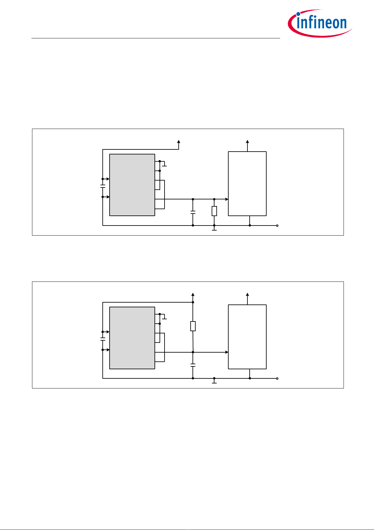
1 Application Circuits
The application circuits in this chapter show the various communication possibilities of the TLE5014.
Figure 1 shows a basic application circuit of a TLE5014 with PWM interface. The pull-down resistor is required
to ensure that the sensor starts with a low level after power-on or reset (PWM starts with a rising edge). If the
sensor is configured in such a way, that the PWM starts with a falling edge, the pull-down has to be replaced
by a pull-up.
Figure 1 Application circuit for TLE5014 with PWM, sensor configured to start with a rising edge of
PWM
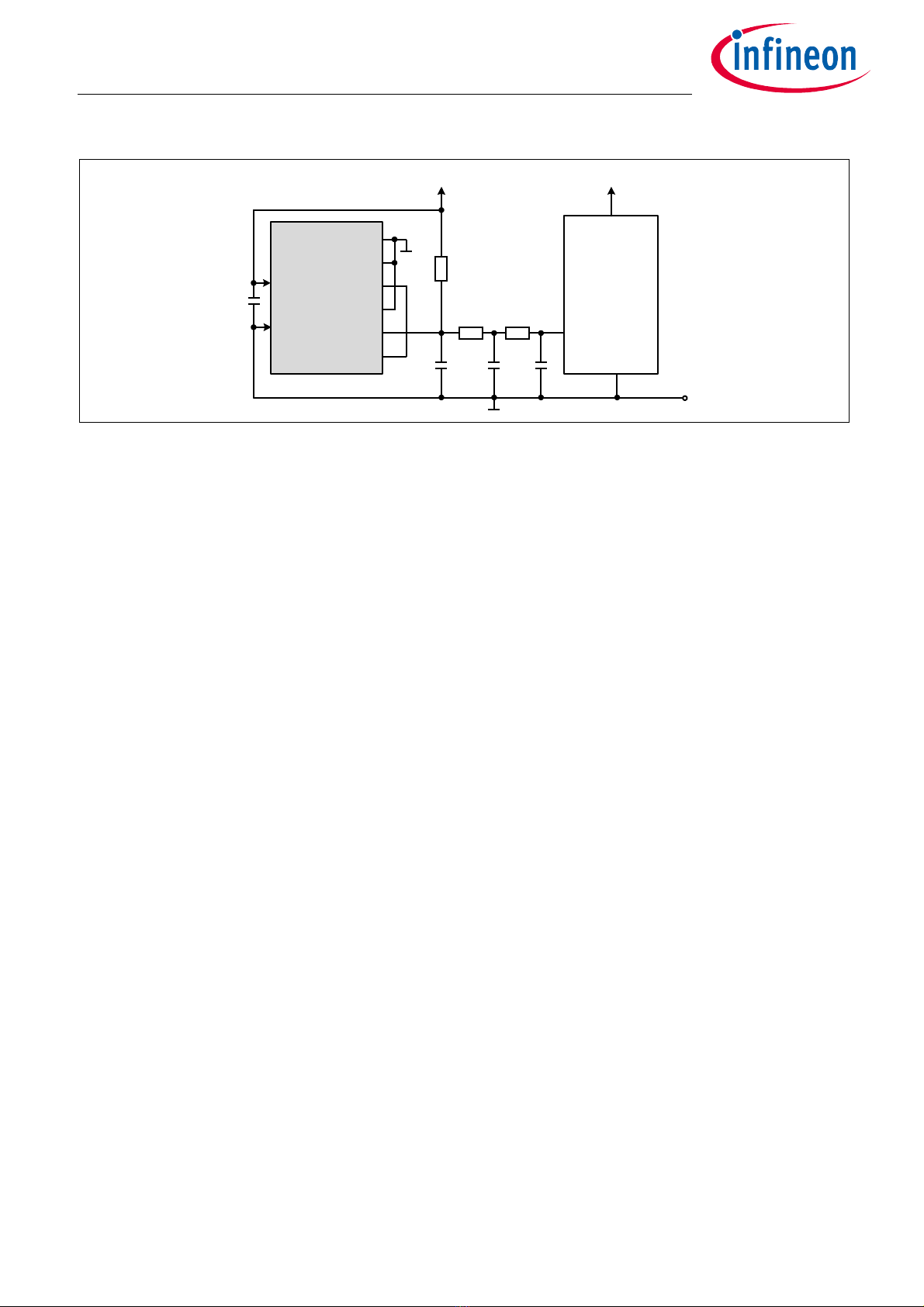
Figure 2 shows a basic application circuit of the TLE5014 with SPC mode.
Figure 2 Application circuit for TLE5014 with SPC, SPC address is configured to be “0” (IF1 and IF2
connected to GND)
The circuit shows the minimum external circuit which is needed to operate the SPC interface. The generation
of the trigger pulse (switch to pull the line low) is not shown. Depending on EMC requirements, additional
circuitry may be required. The value of Cwand Rpare specified in the datasheet.
The TLE5014 can also be used with a SENT interface (Figure 3). The circuit shown is according to the SAE
J2716-2010 SENT specification.
TLE501 4
GND
µController
Master
10 0nF
VDD
VDD
GND
IF1
IF2
IF3
IFA
IFB
IFC
VµC
Rp
PWM
Cw
TLE501 4
GND
µController
Master
10 0nF
VDD
VDD
GND
IF1
IF2
IF3
IFA
IFB
IFC
VµC
Rp
SP C
Cw
User’s Manual 5 Rev. 1.0
2019-03-12
TLE5014
GMR-Based Angle Sensor
Application Circuits
Figure 3 Application circuit for TLE5014 with SENT
TLE501 4
GND
µController
Master
10 0nF
V
DD
V
DD
GND
IF1
IF2
IF3
IFA
IFB
IFC
V
µC
10 k
56 0 10k
68 p 2.2n 10 0p

User’s Manual 6 Rev. 1.0
2019-03-12
TLE5014
GMR-Based Angle Sensor
Interfaces overview
2 Interfaces overview
Depending on the application, the TLE5014 is available with different interfaces:
• PWM (Pulse Width Modulation)
• SPC (Short PWM Code)
• SENT (Single Edge Nibble Transmission)
• SICI (Single-wire Interface for Calibration and Inspection; for programming purpose only)
PWM
The PWM is an unidirectional interface. Only one line is needed in which the angle value is transmitted. The
angle value corresponds to the duty cycle of the signal data. A reserved duty cycle range is implemented which
is used for indication of internal detected device errors. The data duty cycle range and the error duty cycle
range can be programmed via EEPROM setting.
SPC
The SPC is an interface based on the SENT protocol. The ECU (master µC) sends a trigger pulse which triggers
the TLE5014 to transmit the 12-bit angle value. If desired, the temperature can also be transmitted on a slow
channel (short serial message). The SPC also sends a CRC nibble and an end-pulse to terminate the
communication. One line is needed for the transmission and the pins IF1, IF2 and IFC are used to set the slave
number. Up to four slaves can be connected to one ECU; the ECU trigger pulse length will trigger the respective
sensor.
SENT
SENT is a standardized interface described in SAE J2716-2010.
SICI
A PWM based, bidirectional interface which is used for programming purpose only.
Further details on the SENT, SPC and PWM interface can be found in the data sheet of TLE5014.
2.1 PWM Interface Configuration
The following configuration of the PWM interface is possible. Further details are in the EEPROM register
description in Chapter 4.
Table 2 PWM Interface configuration
Parameter EEPROM
Register
Description
PWM data duty cycle range
minimum value
0x0060 This value determines the low value of the duty cycle for
angle transmission. It corresponds to an angle value of 0°
PWM data duty cycle range
maximum value
0x0062 This value determines the high value of the duty cycle for
angle transmission. It corresponds to an angle value of
359.91°
PWM diagnostic duty cycle low 0x0064 This value determines the duty cycle which indicates a
sensor failure detected by the internal safety mechanism

User’s Manual 7 Rev. 1.0
2019-03-12
TLE5014
GMR-Based Angle Sensor
Interfaces overview
Care has to be taken when programming the low and high diagnostic duty cycle that there is no overlap with
the programmed data duty cycle range. In such a case, diagnostic information (e.g. sensor failure) could not
be distinguished from a valid transmitted angle value. It is recommended to add a safety margin between the
diagnostic and the data duty cycle range.
2.2 SPC Interface Configuration
The following table shows the different options for SPC interface configuration. The details for the EEPROM
setting are shown in Chapter 4.3
PWM diagnostic duty cycle high 0x0066 This value determines the duty cycle which indicates a
sensor reset or a sensor start-up error (BIST error)
PWM predevider for PWM period 0x0068 This value is used for PWM frequency adjustment according
to Equation (4.1)
PWM period 0x006A This value is used for PWM frequency adjustment according
to Equation (4.1)
PWM starting edge 0x00A2 This value determines the starting edge of the PWM protocol.
It can be rising or falling. In case a rising edge is selected, the
PWM protocol will start with a HIGH level. In case a falling
edge is selected, it will start with a LOW
Table 3 SPC Interface configuration
Parameter EEPROM
Register
Description
SPC low time 0x00A2 This value can be 5 UT or 3UT.With5UT,theSPCnibbleis
compliant to the SENT specification
Temperature information in SPC
protocol
0x00A2 The SPC frame can contain two additional nibbles for
transmitting the temperature information
Rolling counter 0x00A2 A 4-bit rolling counter (rolling counter nibble) can be
activated which counts the transmitted frames. This is
necessary for functional safety applications to increase the
diagnostic coverage
Rolling counter in CRC 0x00A2 The rolling counter information can be coded in the CRC of
the SPC frame instead of being transmitted as extra nibble.
In this case the rolling counter information has 2 bit only.
This feature reduces overall frame length of the SPC protocol
SPC trigger 0x00A2 Two options are available for the total trigger length. It can
be constant with a length of 90 UT or variable. The variable
trigger length is tlow +12 UT and depends on the trigger low
time tlow. Both settings can be used in a bus configuration as
the address of the sensor is defined by the low time tlow only.
The advantage of the variable trigger length is that the total
frame length can be reduced
Table 2 PWM Interface configuration (cont’d)
Parameter EEPROM
Register
Description

User’s Manual 8 Rev. 1.0
2019-03-12
TLE5014
GMR-Based Angle Sensor
Interfaces overview
SPC address setting in bus mode
The address of the sensor, so that it responds to a corresponding SPC trigger pulse, has to be set in the
EEPROM. All parts delivered from Infineon have the default address of ID = 0 in the EEPROM. Please refer to
description of EEPROM register 0x00A4 in Description EEPROM Address 0x00A4 CRC_CFG for correct setting.
The address of the sensor written to the EEPROM must be identical to the address of the sensor defined via
hard-wiring of the pins IF1, IF2 and IFC. Table 4 shows how the sensor address has to be set using the pins IF1,
IF2, IFC.
Figure 4 shows a SPC frame with constant trigger length of 90UT, a status nibble, 3 data nibbles, a rolling
counter nibble and a CRC nibble. The low time of the trigger nibble determines the address of the sensor.
Figure 4 SPC frame with constant trigger length and rolling counter enabled as additional nibble
SPC short serial message 0x00A2 A short serial message (slow message) can be activated,
which transmits one bit of a 16 bit information in each SPC
frame and thus needs 16 SPC frames for the whole data
transmission.This transmitted information is the
programmed angle base and rotation direction, the chip
temperature and 32 bit of the customer ID.
SPC unit time (UT) 0x00A2 The SPC unit time (UT) can be selected in the range of 1.0 µs
to 3.0 us.
Table 4 SPC Address Configuration
Address IF1 IF2
0GNDGND
1IFCGND
2GNDIFC
3IFCIFC
Table 3 SPC Interface configuration (cont’d)
Parameter EEPROM
Register
Description
Synchronisation
Frame
Trigger Nibble
µC Activity
Sensor Activity
90 UT 56 UT 12 … 27 UT 12 … 27 UT 12 … 27 UT 12 … 27 UT 12 … 27 UT 12 UT
Status Nibble Data Nibble 1 Data Nibble 3Data Nibble 2 CRC End
pulse
12 … 27 UT
Rolling counter

User’s Manual 9 Rev. 1.0
2019-03-12
TLE5014
GMR-Based Angle Sensor
Interfaces overview
SPC status nibble
The 4-bit status nibble of the SPC protocol has different content depending on SPC protocol configuration:
• No short serial message:
• Short serial message (SSM) enabled:
In this configuration, the sensor ID is coded in the CRC and not available in the status nibble. There is also the
option, that the rolling counter is not a dedicated nibble but the information is also coded in the CRC.
Therefore, four different versions of the CRC calculation exist:
• No short serial message (SSM) and rolling counter as nibble
Input data for the CRC calculation are:
STATUS & DATA1 & DATA2 & DATA3 & ROLLING_CNT
• Short serial message (SSM) enabled and rolling counter as nibble
the CRC calculation has to include a special 4-bit “ID-nibble” and is performed with the following input
data:
STATUS & DATA1 & DATA2 & DATA3 & ROLLING_CNT & ID_NIBBLE
ID_NIBBLE = (0 0 ID(MSB) ID(LSB))
• Short serial message (SSM) is disabled and rolling counter is included in CRC (no rolling counter as nibble)
The CRC calculation has to include a special 4-bit “RC-nibble” and is performed with the following input
data:
STATUS & DATA1 & DATA2 & DATA3 & RC_NIBBLE
RC_NIBBLE = (RC(MSB) RC(LSB) 0 0)
• Short serial message (SSM) is enabled and rolling counter is included in CRC (no rolling counter as nibble)
The CRC calculation has to include a special 4-bit “RC_ID-nibble” and is performed with the following input
data:
STATUS & DATA1 & DATA2 & DATA3 & RC_ID_NIBBLE
RC_ID_NIBBLE = (RC(MSB) RC(LSB) ID(MSB) ID(LSB))
Table 5 SPC Status Nibble
Bit Description
0 (LSB) Sensor ID (LSB)
1SensorID(MSB)
2 Internal sensor failure
3 (MSB) Sensor reset or start-up (BIST) failure
Table 6 SPC Status Nibble
Bit Description
0 (LSB) Data bit of SSM
1 Start bit of SSM
2 Internal sensor failure
3 (MSB) Sensor reset or start-up (BIST) failure

User’s Manual 10 Rev. 1.0
2019-03-12
TLE5014
GMR-Based Angle Sensor
Interfaces overview
Synchronization of the Rolling Counter
The first transmitted SPC frame has a rolling counter value of 0. The next frame transmits a rolling counter
value which is incremented by 1. In case the rolling counter is coded in the CRC, it is a 2-bit value. In this
configuration, a synchronization of the counter value (sensor value and counter value in the micro controller)
is required. The following two options are possible:
• Calculate the CRC with the received sensor data and a RC_NIBBLE of RC_NIBBLE = 0000B. Repeat this until
the calculated CRC matches with the transmitted CRC. This frame has the rolling counter value of 0. The
next transmitted frame has the incremented counter value of 1 and so on. As the rolling counter has 2 bit
in case it is coded in the CRC, latest the fourth transmitted frame needs to have a matched CRC. If this is
not the case an error occurred.
• For the first transmitted frame, calculate the four possible CRCs with the RC_NIBBLE values 0000Bto 0011B.
The CRC which is matching the transmitted CRC has the correct rolling counter value. Use this value as
starting value which is incremented with the next received frame.
CRC calculation for SPC protocol
The checksum nibble is a 4-bit CRC of the data nibbles including the status nibble. The CRC is calculated using
a polynomial x4+x3+x2+1 with a seed value of 0101B. The remainder after the last data nibble is transmitted as
CRC. The CRC calculation method is based on “recommended” implementation in the SENT standard 2010.
For this “recommended” implementation, the CRC is calculated based on the input data which is then
augmented with four extra zero bits and an additional CRC calculation step.
Code example:
//Table CRC, Poly=0xD
uint8_t cr4Table[16] = {0, 13, 7, 10, 14, 3, 9, 4, 1, 12, 6, 11, 15, 2, 8, 5};
//Example:
//Status Nibble = 0x6
//Data Nibble = 0x7, 0x4, 0x8, 0x7, 0x4, 0x8
uint8_t nibble[7] = {6, 7, 4, 8, 7, 4, 8};
uint8_t nb_nibble = 0x7;
Table 7 Examples for ID Nibble, RC_Nibble and ID_RC_Nibble calculation
ID RC ID_Nibble RC_Nibble RC_ID_Nibble
00B–0000B––
01B– 0001B––
10B– 0010B––
11B– 0011B––
–00
B–0000
B–
–01
B–0100
B–
–10
B–1000–
–11
B–1100
B–
00B00B– – 0000B
01B01B– – 0101B
10B10B– – 1010B
11B11B– – 1111B

User’s Manual 11 Rev. 1.0
2019-03-12
TLE5014
GMR-Based Angle Sensor
Interfaces overview
//Seed value = 0x5
uint8_t crc = 0x5;
for(uint8_t i=0;i<nb_nibble;i++){
crc = nibble[i] ^ cr4Table[crc];
}
//Final XOR
crc = 0x0 ^ cr4Table[crc];
2.3 SENT Interface Configuration
The following table shows the different options for SENT interface configuration.
SENT Status Nibble
The 4-bit status nibble of the SENT protocol contains the following information:
Table 8 SENT Interface configuration
Parameter EEPROM
Register
Description
SENT low time 0x00A2 This value can be 5 UT or 3 UT. With 5 UT, the nibble is
compliant to the SENT specification
SENT protocol type 0x00A2 Two different SENT implementations can be configured:
Standard SENT: Status nibble, 3 x 4-bit data nibbles, CRC
nibble
Single Secure SENT: Status nibble, 3 x 4-bit data nibbles, 2x4-
bit rolling counter; Inverted data nibble, CRC nibble
Sent short serial message 0x00A2 A short serial message (slow message) can be activated
which transmits one bit of additional information in each
SPC frame. This transmitted information is the programmed
angle base and rotation direction, the chip temperature and
32 bit of the customer ID
SENT error indication 0x00A2 In case of an internal chip error, the error can be indicated
only in the status nibble by setting an error bit or in the status
nibble and also in the SENT data range. In this case an error
code of “4091” is sent. For this option, the data range has not
the full 12-bit resolution but only 1 … 4088 LSB
Sent unit time (UT) 0x00A2 The SENT unit time (UT) can be selected in the range of 1.5 µs
to 3.0 us
Table 9 SENT Status Nibble
Bit Description
0 (LSB) error indication or start-up (BIST) error or sensor reset
1 reserved
2 short serial message bit (data bit)
3 (MSB) short serial message bit (start indication)

User’s Manual 12 Rev. 1.0
2019-03-12
TLE5014
GMR-Based Angle Sensor
Interfaces overview
CRC calculation for SENT protocol
The checksum nibble is a 4-bit CRC of the data nibbles and does not include the status nibble (different to SPC
CRC implementation). The CRC is calculated using a polynomial x4+x3+x2+1 with a seed value of 0101B. The
remainder after the last data nibble is transmitted as CRC. The CRC calculation method is based on
“recommended” implementation in the SENT standard 2010. For this “recommended” implementation, the
CRC is calculated based on the input data (without STATUS nibble) which is then augmented with four extra
zero bits and an additional CRC calculation step.
Code example:
//Table CRC, Poly=0xD
uint8_t cr4Table[16] = {0, 13, 7, 10, 14, 3, 9, 4, 1, 12, 6, 11, 15, 2, 8, 5};
//Example:
//Data Nibble = 0x7, 0x4, 0x8, 0x7, 0x4, 0x8
uint8_t nibble[6] = {7, 4, 8, 7, 4, 8};
uint8_t nb_nibble = 0x6;
//Seed value = 0x5
uint8_t crc = 0x5;
for(uint8_t i=0;i<nb_nibble;i++){
crc = nibble[i] ^ cr4Table[crc];
}
//Final XOR
crc = 0x0 ^ cr4Table[crc];

User’s Manual 13 Rev. 1.0
2019-03-12
TLE5014
GMR-Based Angle Sensor
EEPROM Page Map
3 EEPROM Page Map
The TLE5014 has an EEPROM as non-volatile memory where sensor configuration data can be stored. The
memory is organized in pages, each page contains 8 registers, each register has 16 bit. Some pages and
registers can be accessed by the user and the content can be modified thus changing chip configuration. Care
has to be taken when modifying content of the EEPROM as the device behavior can be changed and no or
wrong output data can be generated. There is no automatic restore functionality where the pre-programmed
status can be recovered.
The EEPROM content is secured by a CRC. In case any content of the EEPROM is changed, the CRC has to be
recalculated and written to the corresponding register, otherwise an error is indicated. The CRC has always be
calculated out of several pages and registers, which are indicated in the description of the corresponding CRC
(Table 10). The algorithm for the CRC calculation is described in Chapter 6.2.3.
The following Table 10 shows the pages and EEPROM registers of each page and their function. A detailed
description of the EEPROM registers and the possible settings can be found in Chapter 4.
The startup value of each configuration register of the TLE5014 is stored in a corresponding EEPROM register,
which can be modified by the user. Table 10 lists the allocation of the user-configurable EEPROM pages.
Care shall be taken when the EEPROM configuration is changed, as not all possible configurations are released
by Infineon. This means, that they can be used for testing purpose but not necessarily for production. All
released configurations can be found in the TLE5014 datasheet.
Table 10 EEPROM page map
Page EEPROM
Register
Name Description Default value of Reg.
0x006 0x0060 OUT_LIM_MIN PWM data duty cycle range minimum
value
0x0062 OUT_LIM_MAX PWM data duty cycle range maximum
value
0x0064 OUT_STAT_L PWM diagnostic duty cycle low
0x0066 OUT_STAT_H PWM diagnostic duty cycle high
0x0068 TMR_PREDIV PWM predevider for PWM period
0x006A TMR_PERIOD PWM period
0x006C – Reserved
0x006E CRC_EEP CRC has to be calculated with following
values: page 0x002 & 0x003 & 0x004 &
0x005 & register 0x0060 & 0x0062 &
0x0064 & 0x0066 & 0x0068 & 0x006A &
0x006C & first byte of 0x006E (bit [15:8] &
0xFF00)

User’s Manual 14 Rev. 1.0
2019-03-12
TLE5014
GMR-Based Angle Sensor
EEPROM Page Map
0x009 0x0090 – Reserved
0x0092 – Reserved
0x0094 – Reserved
0x0096 ACSTAT Activation of internal safety mechanism
0x0098 MOD1 3 V/5 V, pad configuration, LUT options
0x009A MOD2 Lock function for register PWI_MD_USR
0x009C IF123_CFG Pin configuration of pin IF1, IF2, IF3
0x009E IFABC_CFG Pin configuration of pin IFA, IFB, IFC
0x00A 0x00A0 ANG_BASE Angle base & rotation direction
0x00A2 PWI_MD_USR Interface configuration
0x00A4 CRC_CFG Configuration CRC and SPC address;
CRC has to be calculated with following
values: registers 0x0096 & 0x0098 &
0x009A & 0x009C & 0x009E & 0x00A0 &
0x00A2 & first byte of 0x00A4 (bit [15:8] &
0xFF00)
0x00A6 – Reserved
0x00A8 – Reserved
0x00AA – Reserved
0x0AC – Reserved
0x00AE – Reserved
0x00B 0x00B0 LUT_0 Look-up table value for 0°
0x00B2 LUT_1 Look-up table value for 11.25°
0x00B4 LUT_2 Look-up table value for 22.50°
0x00B6 LUT_3 Look-up table value for 33.75°
0x00B8 LUT_4 Look-up table value for 45.00°
0x00BA LUT_5 Look-up table value for 56.25°
0x00BC LUT_6 Look-up table value for 67.50°
0x00BE LUT_7 Look-up table value for 78.75°
0x00C 0x00C0 LUT_8 Look-up table value for 90.00°
0x00C2 LUT_9 Look-up table value for 101.25°
0x00C4 LUT_10 Look-up table value for 112.50°
0x00C6 LUT_11 Look-up table value for 123.75°
0x00C8 LUT_12 Look-up table value for 135.00°
0x00CA LUT_13 Look-up table value for 146.25°
0x00CC LUT_14 Look-up table value for 157.50°
0x00CE LUT_15 Look-up table value for 168.75°
Table 10 EEPROM page map (cont’d)
Page EEPROM
Register
Name Description Default value of Reg.

User’s Manual 15 Rev. 1.0
2019-03-12
TLE5014
GMR-Based Angle Sensor
EEPROM Page Map
0x00D 0x00D0 LUT_16 Look-up table value for 180.00°
0x00D2 LUT_17 Look-up table value for 191.25°
0x00D4 LUT_18 Look-up table value for 202.50°
0x00D6 LUT_19 Look-up table value for 213.75°
0x00D8 LUT_20 Look-up table value for 225.00°
0x00DA LUT_21 Look-up table value for 236.25°
0x00DC LUT_22 Look-up table value for 247.50°
0x00DE LUT_23 Look-up table value for 258.75°
0x00E 0x00E0 LUT_24 Look-up table value for 270.00°
0x00E2 LUT_25 Look-up table value for 281.25°
0x00E4 LUT_26 Look-up table value for 292.50°
0x00E6 LUT_27 Look-up table value for 303.75°
0x00E8 LUT_28 Look-up table value for 315.00°
0x00EA LUT_29 Look-up table value for 326.25°
0x00EC LUT_30 Look-up table value for 337.50°
0x00EE LUT_31 Look-up table value for 348.75°
0x00F 0x00F0 [7:0] CRC_LUT 8-bit CRC for Look-up table; CRC has to
be calculated with following values:
page 0x00B & 0x00C & 0x00D & 0x00E &
first byte of register 0x00F0 (bits [15:8] &
0xFF00)
0x00F2 CUST_ID_0 16-bit of customer ID, will be
transmitted via short serial message
0x00F4 CUST_ID_1 16-bit of customer ID, will be
transmitted via short serial message
0x00F6 CUST_ID_2 16-bit of customer ID
0x00F8 CUST_ID_3 16-bit of customer ID
0x00FA CUST_ID_4 16-bit of customer ID
0x00FC CUST_ID_5 16-bit of customer ID
0x00FE CUST_ID_6 16-bit of customer ID
Table 10 EEPROM page map (cont’d)
Page EEPROM
Register
Name Description Default value of Reg.

User’s Manual 16 Rev. 1.0
2019-03-12
TLE5014
GMR-Based Angle Sensor
EEPROM Page Map
Figure 5 TLE5014 EEPROM bitmap
Page 0x006 1514131211109876543210
0x0060 - -
0x0062 - -
0x0064 - -
0x0066 - -
0x0068 - - ------
0x006A - -
0x006C - - -------------
0x006E - - ------
Page 0x009
0x0090 - - --------------
0x0092 - - --------------
0x0094 - - --------------
0x0096
0x0098
0x009A
0x009C ------
0x009E ------
Page 0x00A
0x00A0 ANG_DIR -
0x00A2
0x00A4 -----AS_NR
0x00A6 - - --------------
0x00A8 - - --------------
0x00AA - - --------------
0x00AC - - --------------
0x00AE - - --------------
Page 0x00B
0x00B0
0x00B2
0x00B4
0x00B6
0x00B8
0x00BA
0x00BC
0x00BE
Page 0x00C
0x00C0
0x00C2
0x00C4
0x00C6
0x00C8
0x00CA
0x00CC
0x00CE
Page 0x00D
0x00D0
0x00D2
0x00D4
0x00D6
0x00D8
0x00DA
0x00DC
0x00DE
Page 0x00E
0x00E0
0x00E2
0x00E4
0x00E6
0x00E8
0x00EA
0x00EC
0x00EE
Page 0x00F
0x00F0 --------
0x00F2
0x00F4
0x00F6
0x00F8
0x00FA
0x00FC
0x00FE
CUST_ID_2
CUST_ID_3
CUST_ID_4
CUST_ID_5
CUST_ID_6
CUST_ID_0
CUST_ID_1
LUT_22
LUT_23
LUT_24
LUT_25
LUT_26
LUT_27
CRC_LUT
LUT_28
LUT_29
LUT_30
LUT_31
LUT_21
LUT_10
LUT_11
LUT_12
LUT_13
LUT_14
LUT_15
LUT_16
LUT_17
LUT_18
LUT_19
LUT_20
LUT_8
LUT_9
LUT_3
LUT_4
LUT_5
LUT_6
LUT_7
TMR_PERIOD
CRC_EEP
LUT_0
LUT_1
LUT_2
ANG_BASE
ACSTAT
MOD1
MOD2
IF123_CFG
IFABC_CFG
PWI_MOD
S_NR_EEP CRC_CFG
OUT_LIM_MIN
OUT_LIM_MAX
OUT_STAT_L
OUT_STAT_H
TMR_PREDIV

User’s Manual 17 Rev. 1.0
2019-03-12
TLE5014
GMR-Based Angle Sensor
EEPROM Register Description
4 EEPROM Register Description
This chapter describes the EEPROM registers which can be accessed via SICI in the EEPROM programming
mode. Further registers needed for EEPROM programming are described in Chapter 7.1.
Care shall be taken that there is no unintended modification of bits. When modifying registers, reserved bits
have to be read and written back with the same value.
4.1 Page 0x006
The page 0x06 is used for the configuration of the PWM protocol. It is only relevant in case PWM is selected as
interface in the register PWI_MD_USR (0x00A2). The following tables EEPROM Register Address 0x0060
OUT_LIM_MIN to EEPROM Register Address 0x006E CRC_EEP show the details.
EEPROM Register Address 0x0060 OUT_LIM_MIN
1514131211109876543210
OUT_LIM_MIN
Field Bits Type Description
OUT_LIM_MIN 13:0
Minimum value of data duty cycle range; 0% … 100% mapped to
0 … 16383
EEPROM Register Address 0x0062 OUT_LIM_MAX
1514131211109876543210
OUT_LIM_MAX
Field Bits Type Description
OUT_LIM_MAX 13:0
Maximum value of data duty cycle range; 0% … 100% mapped to
0 … 16383
EEPROM Register Address 0x0064 OUT_STAT_L
1514131211109876543210
OUT_STAT_L

User’s Manual 18 Rev. 1.0
2019-03-12
TLE5014
GMR-Based Angle Sensor
EEPROM Register Description
Field Bits Type Description
OUT_STAT_L 13:0
Low value of diagnostic duty cycle; 0% … 100% mapped to 0 … 16383
EEPROM Register Address 0x0066 OUT_STAT_H
1514131211109876543210
OUT_STAT_H
Field Bits Type Description
OUT_STAT_H 13:0
High value of diagnostic duty cycle; 0% … 100% mapped to 0 … 16383
EEPROM Register Address 0x0068 TMR_PREDIV
1514131211109876543210
TMR_PREDIV
Field Bits Type Description
TMR_PREDIV 7:0
For calculation of PWM frequency according to Equation (4.1)
EEPROM Register Address 0x006A TMR_PERIOD
1514131211109876543210
TMR_PERIOD
Field Bits Type Description
TMR_PERIOD 13:0
For calculation of PWM frequency according to Equation (4.1)
EEPROM Register Address 0x006E CRC_EEP
1514131211109876543210
CRC_EEP

User’s Manual 19 Rev. 1.0
2019-03-12
TLE5014
GMR-Based Angle Sensor
EEPROM Register Description
The PWM frequency of the PWM output can be programmed with the two parameters TMR_PREDIV and
TMR_PERIOD according to the following Equation (4.1):
(4.1)
Example:
For TMR_PREDIV = 12, TMR_Period = 15384, the PWM frequency calculates to f= 200 Hz.
4.2 Page 0x009
Care has be taken that there is no unintended modification of bits. When modifying registers, reserved bits
have to be read and written back with the same value.
Field Bits Type Description
CRC_EEP 7:0
CRC has to be calculated with following values: page 0x002 & 0x003 &
0x004 & 0x005 & register 0x0060 & 0x0062 & 0x0064 & 0x0066 & 0x0068
& 0x006A & 0x006C & first byte of 0x006E (bit [15:8])
Description EEPROM Register Address 0x0098 MOD1
1514131211109876543210
RST_3
_5
CLK_S
EL
FIR_M
DLUT_MD IFMD_ABC IFMD_
123
Field Bits Type Description
RST_3_5 13
0:BReset comparator set to < 3.0 V
1:BReset comparator set to < 4.2 V
CLK_SEL 12
For test purpose only
FIR_MD 11
Internal update rate of angle calculation:
0:B25.6 µs
1:B51.2 µs
LUT_MD 9:8
Look-up table (LUT) configuration:
00:BLUT disabled
01:BLUT range = 360° (angle steps = 11.25°)
10:BLUT range = 180° (angle steps = 5.625°)
11:BLUT range = 90° (angle steps = 2.813°)
fHz[] 40000000
1 TMR_PREDIV+()TMR_PERIOD()
----------------------------------------------------------------------------------------------
=

User’s Manual 20 Rev. 1.0
2019-03-12
TLE5014
GMR-Based Angle Sensor
EEPROM Register Description
IFMD_ABC 5:4
For test purpose only
IFMD_123 0
For test purpose only
Description EEPROM Register Address 0x009A MOD2
1514131211109876543210
MOD2
Field Bits Type Description
MOD2 15:0
Lock register for 0x00A2. The bits in this registers are connected with a
logical AND function with the corresponding bit in 0x00A2. This means
that a “0” in a bit of register 0x009A prohibits to set a “1” in the
corresponding bit of 0x00A2. Note: The bit will show as “1” in 0x00A2
but has no effect
Description EEPROM Register Address 0x009C IF123_CFG
1514131211109876543210
PAD_
OV_O
FF
PAD_S
PIKE
IF3_O
D
IF3_C
FG
IF2_O
D
IF2_C
FG
IF1_O
D
IF1_C
FG
Field Bits Type Description
PAD_OV_OFF 15
Enable/disable overvoltage functionality. Output deactivated in case
of overvoltage on VDD:
0:BOvervoltage functionality enabled
1:BOvervoltage functionality disabled
PAD_SPIKE 14
Activate spike filter for input stage:
0:BSpike filter disabled
1:BSpike filter enabled
IF3_OD 11
IF3 open drain enable:
0:BDisable (Push-Pull)
1:BEnable (Open Drain)
Field Bits Type Description
This manual suits for next models
5
Table of contents
Other Infineon Accessories manuals

Infineon
Infineon TLE493D-A2B6 User manual

Infineon
Infineon TLI4970-D050T4 CurrentSense Shield2Go User manual

Infineon
Infineon SP37 Instruction and safety manual

Infineon
Infineon TLE5501 Series User manual

Infineon
Infineon TLI4970 Mounting instructions

Infineon
Infineon XENSIV BGT60TR13C User manual

Infineon
Infineon TLE4997 User manual

Infineon
Infineon TLI493D-A2B6 User manual

Infineon
Infineon XENSIV TLI4971 Operating instructions


