Infineon WLC1115 User manual

User Guide Please read the Important Notice and Warnings at the end of this document 002-35126 Rev. **
www.infineon.com page 1 of 25 2022-05-10
WLC1115 MP-A11 15-W wireless power
transmitter (REF_WLC_TX15W_C1) user guide
About this document
Scope and purpose
This document is a user guide for the WLC1115 MP-A11 15-W wireless power transmitter reference solution
(REF_WLC_TX15W_C1). It is a Qi 1.3.2 certified solution (Qi Id: 12383) and supports up to 15-W charging. The
reference board demonstrates the capabilities and features of the Infineon WLC1115 wireless charging
transmitter controller. WLC1115 is a highly integrated wireless power transmitter with an integrated USB Type-
C Power Delivery (PD) controller, certified for USB PD 3.1 specification (USB-IF TID: 7531).
You can see the relevant sections based on your requirement:
•Introduction –Provides basic information on the reference board, including details about the interfaces
•WLC1115 software tool –Provides an overview of the Wireless Charging Configuration Utility software
•WLC1115 wireless power transmitter system design –Explains the reference board architecture and
system design details
•Reference board operation –Describes operating the reference board as a wireless power transmitter,
configuring the system-level parameters, downloading the firmware, and capturing the debug log.
Intended audience
The document is intended for the users of WLC1115 15-W wireless power transmitter reference board
(REF_WLC_TX15W_C1).
Related documents
[1] Product webpage:
−Wireless charging ICs
[2] Reference board webpage
−REF_WLC_TX15W_C1 wireless charging (WLC) MP A11 power transmitter

User Guide 2 of 25 002-35126 Rev. **
2022-05-10
WLC1115 MP-A11 15-W wireless power transmitter
(REF_WLC_TX15W_C1) user guide
Table of contents
Table of contents
About this document....................................................................................................................... 1
Table of contents............................................................................................................................ 2
Safety information ......................................................................................................................... 3
1Introduction .......................................................................................................................... 4
1.1 Contents ..................................................................................................................................................4
1.2 Downloading the kit documents and hardware design files.................................................................4
1.3 Board details ...........................................................................................................................................5
2WLC1115 software tool ........................................................................................................... 6
2.1 Wireless Charging Configuration Utility .................................................................................................6
3WLC1115 wireless power transmitter system design.................................................................. 7
3.1 REF_WLC_TX15W_C1 MP A11 15W power transmitter board................................................................8
3.1.1 Board connectors.............................................................................................................................10
3.1.2 Test points........................................................................................................................................11
4Reference board operation.....................................................................................................12
4.1 Wireless charging operation .................................................................................................................12
4.1.1 Hardware connection ......................................................................................................................12
4.2Configuring and downloading the firmware........................................................................................14
4.2.1 USB CC communication-based set-up ............................................................................................14
4.2.2 I2C communication-based set-up ...................................................................................................14
4.3 Capturing debug logs on the WLC reference board.............................................................................15
Appendix A: Enabling DC input power based wireless charging operation on the REF_WLC_TX15W_C1
reference board ....................................................................................................................20
Technical support..........................................................................................................................23
Revision history.............................................................................................................................24

User Guide 3 of 25 002-35126 Rev. **
2022-05-10
WLC1115 MP-A11 15-W wireless power transmitter
(REF_WLC_TX15W_C1) user guide
Safety information
Safety information
The REF_WLC_TX15W_C1 reference board is intended for use as an evaluation platform for hardware or
software in a laboratory environment. The board is an open-system design, which does not include a shielded
enclosure. Due to this reason, the board may cause interference to other electrical or electronic devices in close
proximity. In such cases, take adequate preventive measures. Also, do not use this board near any medical
equipment or RF devices.
Attaching additional wiring to this product or modifying the product operation from the factory default may
affect its performance and cause interference with other apparatus in the immediate vicinity. If such
interference is detected, suitable mitigating measures must be taken.
The REF_WLC_TX15W_C1 reference board contains ESD-sensitive devices.
Electrostatic charges readily accumulate on the human body and any equipment,
which can cause a discharge without detection. Permanent damage may occur to
devices subjected to high-energy discharges. Proper ESD precautions are
recommended to avoid performance degradation or loss of functionality. Store
unused REF_WLC_TX15W_C1 reference boards in the protective shipping package.
General safety instructions
ESD protection
ESD can damage boards and associated components. Infineon recommends that the user perform procedures
only at an ESD workstation. If an ESD workstation is unavailable, use appropriate ESD protection by wearing an
antistatic wrist strap attached to the chassis ground (any unpainted metal surface) on the board when handling
parts.
Handling boards
The boards provided with the REF_WLC_TX15W_C1 reference board are sensitive to ESD. When removed from
the casing, this applies to the boards supplied with a plastic casing. Hold the boards only by the edges. Place it
on a grounded, static-free surface after removing a board from the box/casing. Use a conductive foam pad, if
available. Do not slide the board over any surface.
Do’s and don’ts
•Do not touch the inverter output area marked below while the reference board is
in use. The components in this area may operate at a voltage higher than 30 V
•Keep the coil area of the reference board clear from any metallic debris
•Monitor the coil interface’s surface temperature during prolonged usage

User Guide 4 of 25 002-35126 Rev. **
2022-05-10
WLC1115 MP-A11 15-W wireless power transmitter
(REF_WLC_TX15W_C1) user guide
Introduction
1Introduction
This document is a user guide for the WLC1115 MP-A11 15-W wireless power transmitter reference solution
(REF_WLC_TX15W_C1). This solution consists of the reference board, firmware, and software utility called as
the Wireless Charging Configuration Utility.
Infineon’s WLC1115 based 15-W wireless power transmitter reference board REF_WLC_TX15W_C1 is a highly
integrated, Qi compliant transmitter design with an MP-A11 type transmitter coil. The REF_WLC_TX15W_C1
board works with WPC-certified wireless receivers by taking power from a type-C PD adapter. The input voltage
will be automatically configured to 9-V, 15-V or 20-V based on load power requirements of receiver and PD
capability. A two-switch buck regulator topology, powered by PD input, is used to provide the regulated input
voltage to the full-bridge inverter, driving the resonance tank (resonance capacitor and transmitter coil).
The WLC1115 can support variable inverter input voltage control and variable WPC operating frequencies
control for inverter to optimize operation with WPC receivers. For the MP-A11 transmitter coil, variable inverter
input voltage control is used by the WLC1115. WLC1115 has integrated gate drivers for the buck and inverter
power supplies necessary for wireless transmitter applications. WLC1115 supports a wide input voltage range
and offers many programmable features for creating distinct wireless transmitter solutions.
Visit the product webpage [1] to understand the capabilities of the WLC1115 controller in more detail.
Note: Infineon offers Qi v1.3.2 EPP certified reference solution with several configurable parameters via the
Wireless Charging Configuration Utility for system-specific enhancements. However, the end product Qi
certification is the product manufacturer’s responsibility.
1.1 Contents
The WLC1115 15-W wireless power transmitter reference board package contains the following:
•WLC1115 15-W wireless power transmitter reference board (REF_WLC_TX15W_C1) (1 no.)
•USB-C power adapter (1 no.)
•USB Type-C cable (1 no.)
•Qi-compatible receiver (1 no.)
•Host Programming Interface (HPI) dongle for programming/debugging (1 no.)
•USB micro-B cable (1 no.)
•Quick start guide (1 no.)
•Jumper wires (4 nos.)
The following items may be required for evaluating the wireless power transmitter capabilities of the reference
board. Note that these are not included in the reference board package.
•Qi- compatible phone
•Windows PC running Windows OS 10 or higher to run the Wireless Charging Configuration Utility
1.2 Downloading the kit documents and hardware design files
The documents and the hardware design files for REF_WLC_TX15W_C1 can be downloaded from the
REF_WLC_TX15W_C1 reference board webpage [2]. The documents include a quick start guide, test report and
user guide (this document). The hardware design files package include schematic, BOM, and layout files.


User Guide 6 of 25 002-35126 Rev. **
2022-05-10
WLC1115 MP-A11 15-W wireless power transmitter
(REF_WLC_TX15W_C1) user guide
WLC1115 software tool
2WLC1115 software tool
2.1 Wireless Charging Configuration Utility
The WLC1115 controller is a fully programmable controller allowing users to configure the firmware parameters
and store them in its internal flash memory. The Wireless Charging Configuration Utility is a Microsoft Windows
application developed by Infineon to guide the WLC11115 user through the process of configuring and
programming the WLC11115 device. The utility allows users to:
1. To read the firmware configuration data from the REF_WLC_TX15W_C1 reference board and modify it or
create a new configuration from the scratch
2. Program the resulting configuration data onto the target WLC1 device or program the complete firmware
WLC1115 controller supports programming over I2C and CC interfaces. Usage of the Wireless Charging
Configuration Utility requires the HPI dongle hardware, which is included in the reference design package.
Figure 2 Wireless Charging Configuration Utility
Visit the product webpage [1] to download the latest version of Wireless Charging Configuration Utility.

User Guide 7 of 25 002-35126 Rev. **
2022-05-10
WLC1115 MP-A11 15-W wireless power transmitter
(REF_WLC_TX15W_C1) user guide
WLC1115 wireless power transmitter system design
3WLC1115 wireless power transmitter system design
The WLC1115 wireless transmitter unit supports wireless charging of Qi compliant wireless receivers and
phones. The transmitter supports BPP and EPP types wireless receivers and complies with the 1.3.2 version of
the Qi specficiation.
The interconnection of REF_WLC_TX15W_C1 with source and receivers is shown in Figure 3. The recommended
DC input source configurations are listed in Table 1.
Figure 3 WLC1115 kit interconnection
Table 1 Input source for the EVK
DC input source
REF_WLC_TX15W_C1 requirement
USB Type-C and PD
9 V, 3 A
15 V, 2 A
20 V, 1.5 A
DC power supply
Variable DC voltage type
9 V to 20 V, 3 A output capacity
USB PD legacy charging protocols,
such as QC 2.0/3.0 and AFC
USB Type-C connector; 9 V-12 V
Note:
1. The kit is configured to operate with USB PD input by default. Contact Infineon Technical support to get the
firmware that supports DC input or QC/AFC adaptor based operation.
2. The dc power supply polarity should not be reversed
3. Customers should acquire their own licensing for QC/AFC support

User Guide 8 of 25 002-35126 Rev. **
2022-05-10
WLC1115 MP-A11 15-W wireless power transmitter
(REF_WLC_TX15W_C1) user guide
WLC1115 wireless power transmitter system design
3.1 REF_WLC_TX15W_C1 MP A11 15W power transmitter board
The REF_WLC_TX15W_C1 MP A11 15-W transmitter board implements the power stage and control of wireless
power transfer system. The transmitter board architecture is shown in Figure 4.
Figure 4 REF_WLC_TX15W_C1 power transmitter reference board architecture
The following are key features of the reference board:
1. Qi 1.3.2 compliance
2. Robust ASK and FSK in-band communication between transmitter and receiver
3. Integrated foreign object detection based on system parameters like Q-factor and power loss
4. Type-C PD Input with PD compliance
5. Wide input voltage ranges from 4.5 V to 24 V
6. Integrated buck converter gate drive and control, operating at a switching frequency of 400 kHz
7. Integrated gate drive for full-bridge inverter operating at 127.7 kHz switching frequency
8. MP-A11 coil with variable Inverter input voltage control
9. Peak efficiency of greater than 83% at full load with WRM483265-10F5-12V-G
The reference board contains the following key sections:
1. Input connector –The board can be powered using a USB-C power adapter over the USB Type-C connector
(J3). There is also an option for a DC power supply connection (J6). See Appendix A to understand the
procedure for powering the reference board using a DC supply. Contact Infineon Technical support to
enable the operation of the reference board using QC/AFC adaptor
2. Buck stage –The buck power stage regulates VBRG voltage to control the power to the receiver. The buck
stage operates at a 400-kHz frequency in forced continuous conduction mode (FCCM). The VBRG is
regulated from 3-V to 18-V based on receiver type and load. Based on the VBRG value, the USB PD contract
(PVIN_0) dynamically varies between 9-V, 15-V, and 20-V during power delivery to optimize efficiency. When
there is no receiver on the interface surface, the USB PD contract is set to 5-V

User Guide 9 of 25 002-35126 Rev. **
2022-05-10
WLC1115 MP-A11 15-W wireless power transmitter
(REF_WLC_TX15W_C1) user guide
WLC1115 wireless power transmitter system design
3. Inverter stage –The full-bridge inverter (Q1 to Q4) is operated at a fixed frequency of 127.7-kHz to drive the
resonant tank formed by the transmitter coil (Lr) and resonant capacitors (Cr). The coil voltage feedback
(COIL-SNS) is used for Q-factor estimation and ASK demodulator circuits
4. Transmitter coil assembly –The transmitter coil is MP-A11 type with specifications per Qi standards. The
coil is mounted on a separate coil PCB. An acrylic sheet forms the interface surface of the transmitter. The
coil mounting adhesive, spacers, and acrylic thickness are selected such that the distance between coil top
surface to interface surface is approximately 3.35-mm (Qi specification –3.5 ± 1 mm). See Figure 5 for coil
assembly details
.dz
PCB
Spacer
Acrylic
Coilassembly
Adhesive
PCB thickness – 1.6mm
Acrylic thickness – 1.78mm
Spacer height – 4.8mm
PCB + adhesive + Coil assembly – 4.9mm
Dz gap – 3.35mm
Figure 5 MP A11 transmitter coil assembly
5. WLC1115-68LQXQ –The WLC1115 is a single controller unit to control the transmitter coil and USB-PD
interface. The WLC1115 simplifies the transmitter board architecture with inbuilt gate drivers for buck and
inverter stage, inbuilt LDO for logic and core power, and more features. With an on-chip 32-bit Arm® Cortex®-
M0 processor, 128-kB flash, 16-kB RAM, and 32-kB ROM, the firmware supporting the complete Qi and USB
PD state machine logic can be programmed onto WLC1115
6. ASK demodulator –The ASK demodulator is based on coil voltage and bridge current. The demodulated
signal from both paths is processed through a dual opamp-based gain stage and a comparator (U1) and
decoded by the WLC1115 controller
7. SLS32AIA020U3USON10 –The authentication requirements for the Qi 1.3.2 is realized using a security
controller from Infineon. The OPTIGA™ Trust comes with full system integration for the cost-effective and
seamless authentication deployment, and it is interfaced to WLC1115 over I2C
8. Q-factor estimation –The Q-factor estimation from coil voltage is performed by WLC1115 through the
signal at Q_COMP. The coil voltage is processed through a blocking capacitor, voltage divider, and clamping
diode to feed to the WLC1115 controller for Q-factor estimation
9. Status indication –The firmware indicates the various system states or events using the dual-color (red
and blue) status LED (LED1). See Reference board operation to understand more details

User Guide 10 of 25 002-35126 Rev. **
2022-05-10
WLC1115 MP-A11 15-W wireless power transmitter
(REF_WLC_TX15W_C1) user guide
WLC1115 wireless power transmitter system design
3.1.1 Board connectors
The transmitter board has power and signal connectors for operation and monitoring the wireless power
transfer. The function of each connector is listed in Figure 6.
Table 2 REF_WLC_TX15W_C1 board connectors
Connector
Type
Description
J3
Power
USB Type-C connector for DC input through a USB-C power
adaptor or QC/AFC type AC/DC adaptor *
This connector is also used to download configuration
data/firmware from the Wireless Configuration Utility through
HPI dongle over the Type-C CC lines. For more information, see
section 4.2.
J6
Power
SMD connector option for DC input through a variable DC power
supply *
J1
Signal
Debug serial port. Connect to an HPI dongle (which is provided
as part of the reference board package) to view system status on
a PC using a terminal emulator software (Tera Term, Putty, and
so on). The data is sent at 1-M baud rate.
J2
Signal
SWD connector. This connector is used to download
configuration data/firmware from Wireless Configuration Utility
through an HPI dongle over I2C lines. For more information, see
section 4.2.
L3
Power
Terminals for transmitter coil connection
* Do not power the transmitter board from both J3 and J6 simultaneously
+
_
DC power
supply
USB Type-C
adaptor
OR
PsoC
programmer
TxGND
To PC through USB to serial converter
To coil
Figure 6 REF_WLC_TX15W_C1 power transmitter board power and signal connections
I2C
SWD connector

User Guide 11 of 25 002-35126 Rev. **
2022-05-10
WLC1115 MP-A11 15-W wireless power transmitter
(REF_WLC_TX15W_C1) user guide
WLC1115 wireless power transmitter system design
3.1.2 Test points
The test points in the REF_WLC_TX15W_C1 MP A11 power transmitter board assist in monitoring and
debugging of the wireless power transfer system. The list of test points and their functionality is covered in
Table 3.
Table 3 List of test points on REF_WLC_TX15W_C1
Test point name
Section
Descritpion
USB-IN
Power
Input power positive rail
USB-GND
Power
Input power ground rail
PVIN_0
Power –Buck
Input positive rail to buck converter after common
mode choke
VBRG_0
Power –Buck
Buck stage output
SW1_0
Power –Buck
Buck stage switching node
HG1_0
Signal –Buck
Buck stage high side MOSFET (M11) gate signal
LG1_0
Signal –Buck
Buck stage low side MOSFET (M12) gate signal
VBB_1
Power –Inverter
Buck stage output after the buck output current sense
resistor
COIL_SNS
Power –Inverter
Coil voltage; Transmitter coil and resonant capacitor
junction point
PWM_OUT
Signal –Inverter
Inverter stage PWM signal
HG1_1
Signal –Inverter
Inverter bank 1 high side MOSFET (M15) gate signal
LG1_1
Signal –Inverter
Inverter bank 1 low side MOSFET (M16) gate signal
HG2_1
Signal –Inverter
Inverter bank 2 high side MOSFET (M13) gate signal
LG2_1
Signal –Inverter
Inverter bank 2 high side MOSFET (M14) gate signal
Q_COMP
Signal –Q-factor
Scaled coil voltage (For Q-factor measurement)
ASK_OUT
Signal –ASK demodulator
ASK demodulator output from WLC1115 to
amplification stage
OPAMP_GAIN
Signal –ASK demodulator
ASK demodulator gain stage amplifier output
CMP_REF
Signal –ASK demodulator
ASK demodulator comparator reference signal
OPAMP_CMP
Signal –ASK demodulator
ASK demodulator comparator output; digital signal to
WLC1115
VIN
Power –WLC1115
Power input to WLC1115
VDDD
Power –WLC1115
WLC1115 internal 5-V LDO output
VCCD
Power –WLC1115
WLC1115 internal 1.8V core LDO output
CLK_IN
Signal –WLC1115
Clock signal from externa oscillator (Applicable for
operation with external oscillator only)
Q_COMP
Signal –WLC1115
Signal used by WLC1115 for Q-factor estimation
GND1, GND2
Power
Power side ground points
GND
Signal
Control side ground point
Note: For more information, see the reference board’s schematic.
User Guide 12 of 25 002-35126 Rev. **
2022-05-10
WLC1115 MP-A11 15-W wireless power transmitter
(REF_WLC_TX15W_C1) user guide
Reference board operation
4Reference board operation
This section explains the wireless charging operation, configuring or updating the firmware parameters, and
programming the updated configuration data to the WLC1115-68LQXQ IC.
4.1 Wireless charging operation
4.1.1 Hardware connection
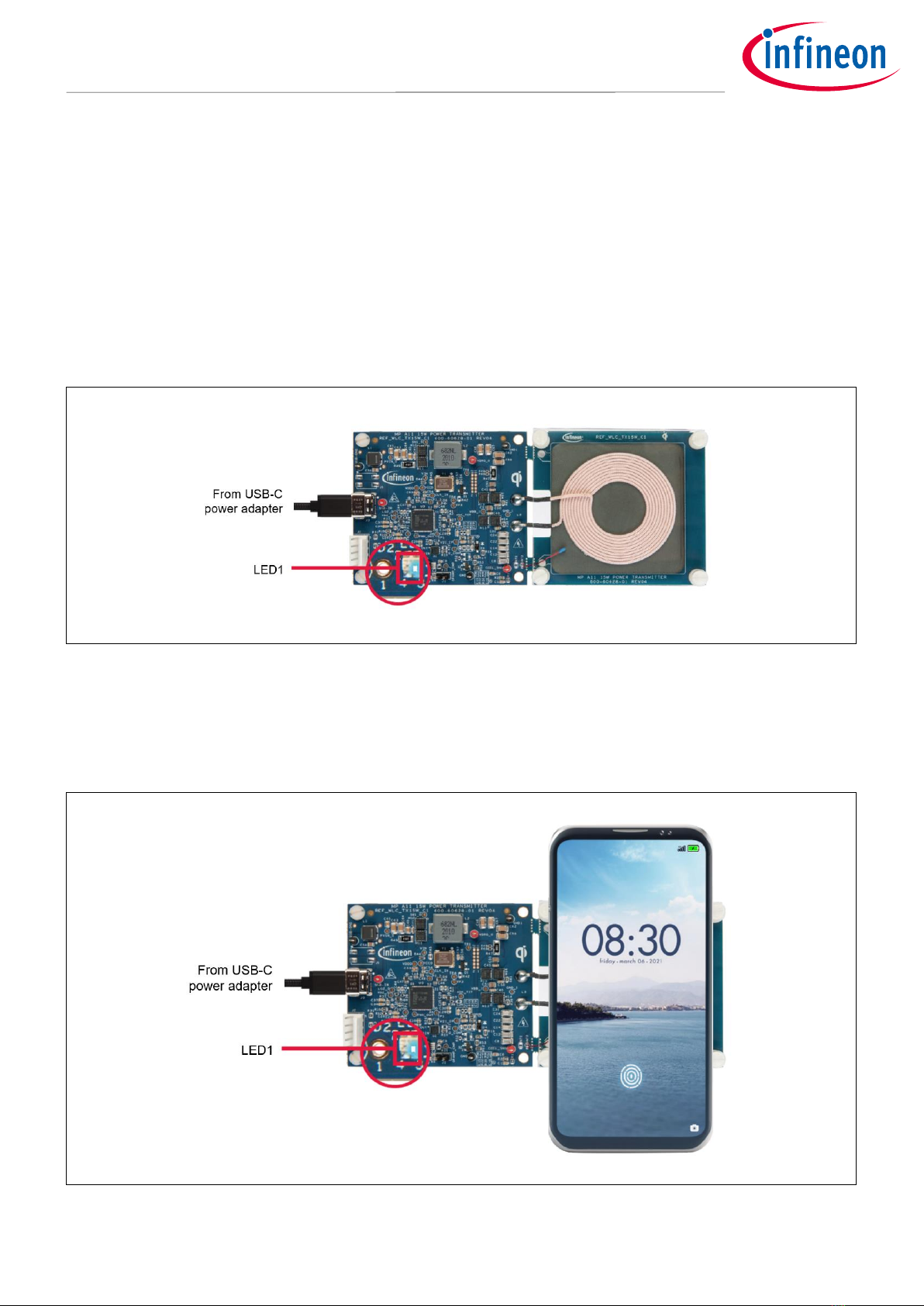
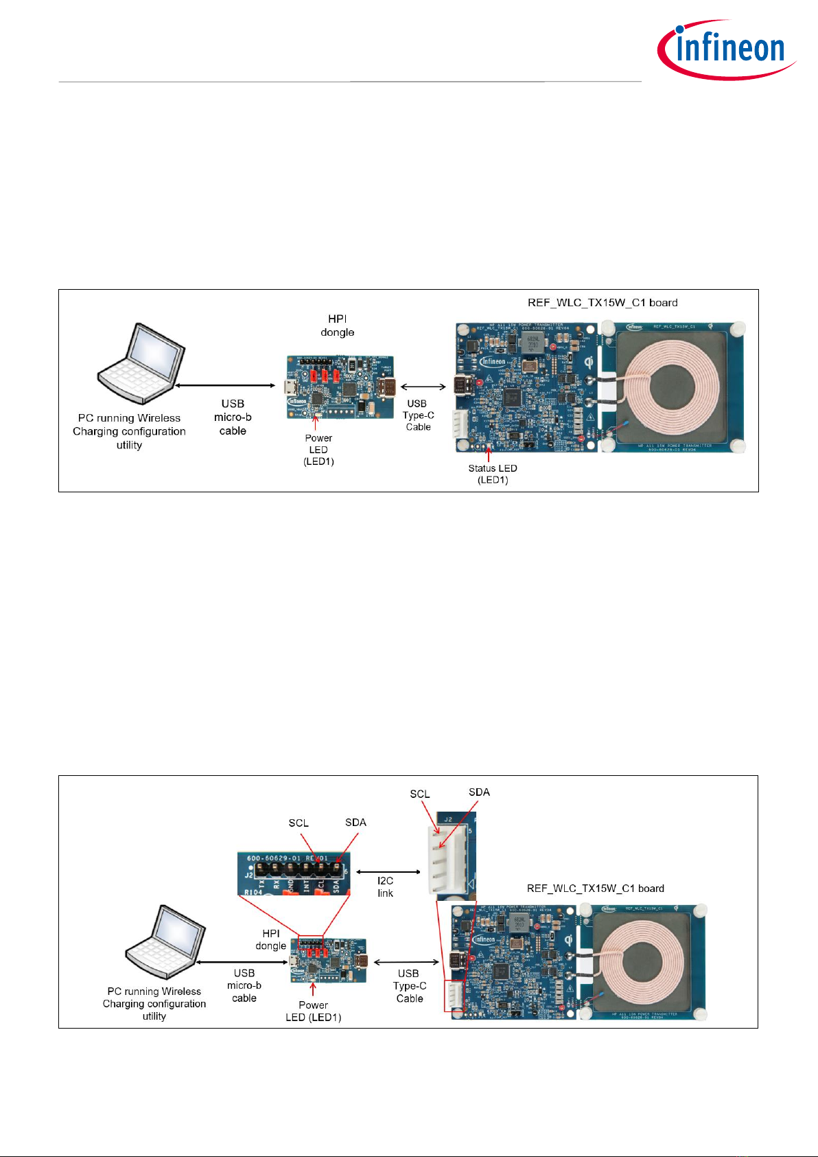
1. Connect the USB-C power adapter to the USB Type-C connector (J3) of the reference board
2. Confirm that the status LED (LED1) blinks five times in blue and red. Now the board is ready for use
Figure 7 Powering the WLC reference board
3. Place the (phone or receiver) to be charged on the Tx interface surface of the reference board, as shown in
Figure 8. The status LED (LED1) glows blue when charging is in progress
4. Observe that the status LED turns OFF when the phone/receiver is removed from the Tx interface surface or
once the phone is fully charged (100%)
Figure 8 Powering the WLC reference board

User Guide 13 of 25 002-35126 Rev. **
2022-05-10
WLC1115 MP-A11 15-W wireless power transmitter
(REF_WLC_TX15W_C1) user guide
Reference board operation
Note: The status LED will continue to glow blue if the phone remains in trickle charging mode after the
battery is fully charged.
Table 4 describes the status LED indications for various system states.
Table 4 System states and status LED indications
Note: The REF_WLC_TX15W_C1 reference board with factory default firmware may exhibit timeout
bound retry of Qi power contract under extremely noisy ASK modulated signal conditions with
some phones/receivers. Such behavior does not affect wireless charging performance. See the
REF_WLC_TX15W_C1 reference board’s test report to get more details about the phone charging
cycle, ASK demodulation, and Qi 1.3.2 compliance test results. This report can be downloaded
from the REF_WLC_TX15W_C1 reference board webpage [2].
See Table 5 for troubleshooting the potential issues faced while operating the WLC 15W Tx reference board.
Table 5 Troubleshooting of the WLC 15W Tx reference board operation
#
Issue
Possible cause
Fix
1
The phone is not charging
when placed on the interface
surface of the WLC reference
board.
The phone may not be a
Qi-certified phone.
Check with the phone manufacturer on
the Qi certification. Get a Qi-certified
phone.
2
The phone is charging at slow
rate.
The phone may not
support Qi’s EPP
capability
Check with the phone manufacturer on
support for EPP capability. Get a phone
which can support EPP to charge at 15
W.
Note: The REF_WLC_TX15W_C1 reference board is by default loaded with a firmware that supports USB
PD based power input. However, the reference board can be powered using a DC supply, requiring
a different firmware. See Appendix A to understand the procedure for powering the WLC1115
referecne board using DC input.
System state
Status LED indication
Idle state
No LED indication
Qi digital ping phase
Blinks blue
Power delivery in progress
Glows blue
Power delivery/charge complete
No LED indication
Foreign object (FO) detected
Glows red until FO is removed
Fault during power transfer
Glows red until the fault is cleared
Aburpt end of power transfer (EPT) initiated by the
receiver
Blinks red
User Guide 14 of 25 002-35126 Rev. **
2022-05-10
WLC1115 MP-A11 15-W wireless power transmitter
(REF_WLC_TX15W_C1) user guide
Reference board operation
4.2 Configuring and downloading the firmware
WLC1115 IC is a programmable controller which supports downloading the updated/modified configuration
data and the firmware over USB CC or I2C communication.
4.2.1 USB CC communication-based set-up
Figure 9 describes the set-up to download configuration data or firmware over the USB CC interface of the
WLC1115 controller.
Figure 9 USB CC communication-based set-up
Execute the following procedure to create the set-up:
1. Connect the HPI dongle to the reference board using the USB Type-C cable
2. Connect the HPI dongle to the PC using a USB micro-B cable
3. The Power LED (LED1) on HPI Dongle glows blue, and the status LED (LED1) on the WLC1115 reference board
blinks in blue and red five times
4. Now the set-up is ready for use by the Wireless Charging Configuration Utility
4.2.2 I2C communication-based set-up
Figure 10 describes the set-up to download configuration data or firmware over the I2C interface of the
WLC1115 controller.
Figure 10 I2C communication-based set-up

User Guide 15 of 25 002-35126 Rev. **
2022-05-10
WLC1115 MP-A11 15-W wireless power transmitter
(REF_WLC_TX15W_C1) user guide
Reference board operation
Execute the following procedure to create the set-up
1. Establish an I2C connection between the WLC1115 reference board and HPI dongle by connecting the two
jumper wires
a) Connect a jumper wire between SCL pin of HPI dongle (pin no. 5 of J2 header) and HPI_I2C_SCL pin of
WLC1115 reference board (pin no. 4 of J2 header)
b) Connect a jumper wire between SDA pin of HPI dongle (pin no. 6 of J2 header) and HPI_I2C_SCL pin of
WLC1115 reference board (pin no. 5 of J2 header)
2. Connect the HPI dongle to the PC using a USB micro-B cable
3. The Power LED (LED1) on HPI Dongle glows blue
4. Connect the HPI dongle to the reference board using the USB Type-C cable. The status LED (LED1) on the
WLC1115 reference board blinks in blue and red five times
5. Now the set-up is ready for use by the Wireless Charging Configuration Utility
See the Wireless Charging Utility user guide to understand the procedure to configure the various firmware
parameters and the procedure to download the configuration or firmware. The user guide can be accessed
from the Help menu of the utility.
4.3 Capturing debug logs on the WLC reference board
This section explains the procedure to capture the debug logs sent on the serial port of the
REF_WLC_TX15W_C1 reference board at various stages of the operation. This feature helps to understand the
internal operation of the firmware in addition to the Status LED indication available on the board.
Prerequisites:
•Ensure that the following items as part of the REF_WLC_TX15W_C1 package are available:
−REF_WLC_TX15W_C1 board (Rev04 and above)
−HPI Dongle (Rev02 and above)
−USB Type-C cable
−USB Micro-B cable
−Jumper wires
•Get a Windows-based PC to run a serial port-based data logging tool, such as Tera Term
•To capture the debug log, do the following steps:
1. Install data logging software on the PC
•Download a data logging tool, such as Tera Term, and install it on the PC
2. Enable debug log in the firmware
a) Download the Wireless Charging Utility package from Infineon’s WLC product webpage [1] and install it on
the PC
b) Create the USB CC communication-based (Figure 9) or I2C communication-based (Figure 10) hardware
set-up to configure the firmware using Wireless Charging Configuration Utility
c) Open the Wireless Charging Configuration Utility from the Start menu in Windows
d) Confirm that the reference board is selected under the Device Selection tab, as shown in Figure 11

User Guide 16 of 25 002-35126 Rev. **
2022-05-10
WLC1115 MP-A11 15-W wireless power transmitter
(REF_WLC_TX15W_C1) user guide
Reference board operation
Figure 11 Selective device in Wireless Charging Configuration Utility
e) Click Tools > Read from Device or select the Read from Device option from the home panel. This enables
the user to read the configuration from the device
f) The debug log can be enabled by configuring the following parameters in the transmitter “Profile” page in
the Wireless Charging Configuration Utility (see Figure 12)
•Enable Critical log enable
•Enable Message log enable
•Set Debug log to Level 1
Figure 12 Profile page settings for enabling debug log
g) Select the device in the Device Selection tab and select Tools > Configure Device or click on the configure
device icon present on the home panel. Save the updated configuration to a file
h) In the Configure Device dialog box, specify the path of the updated configuration file and click Program,
as shown in Figure 13

User Guide 17 of 25 002-35126 Rev. **
2022-05-10
WLC1115 MP-A11 15-W wireless power transmitter
(REF_WLC_TX15W_C1) user guide
Reference board operation
Figure 13 Device configuration dialog
Wait until the updated configuration file gets downloaded, as shown in Figure 14
Figure 14 Successful download of configuration file
i) Dismantle the hardware set-up
3. Debug log capture set-up
a) Do the following connections using jumper wires to establish a serial connection between the
REF_WLC_TX15W_C1 board and the HPI dongle:
•Connect a jumper wire between the UART_Tx pin of J1 of REF_WLC_TX15W_C1 board and Rx pin of J2
header on HPI dongle board
•Connect a jumper wire between the GND pin of J1 of the REF_WLC_TX15W_C1 board and the GND pin of the
J2 header on the HPI dongle board
b) Connect REF_WLC_TX15W_C1, HPI dongle, and PC as shown in Figure 15

User Guide 18 of 25 002-35126 Rev. **
2022-05-10
WLC1115 MP-A11 15-W wireless power transmitter
(REF_WLC_TX15W_C1) user guide
Reference board operation
Figure 15 Set-up for capturing debug log
4. Capture debug logs
a) Open the Tera Term on the Windows PC and select the virtual serial port listed on the Tera Term tool
b) Set the baud rate to 1000000. Set the remaining settings as default, as shown in Figure 16
Figure 16 Tera Term settings
c) Supply power to the REF_WLC_TX15W_C1 board using the USB-C power adapter and recreate the usage
condition during which the debug logs need to be captured. The log data is displayed on the Tera Term as
shown in Figure 17

User Guide 19 of 25 002-35126 Rev. **
2022-05-10
WLC1115 MP-A11 15-W wireless power transmitter
(REF_WLC_TX15W_C1) user guide
Reference board operation
Figure 17 Debug log output
d) Save the log into a file from Tera Term
e) Contact Infineon technical support with the captured log files if additional support is required
5. Disable debug log in the firmware
Revert these changes in firmware to default on completion of the process. debug log consume processor
resource, and it is recommended to disable debug log for optimal performance of the WLC power transmitter.

User Guide 20 of 25 002-35126 Rev. **
2022-05-10
WLC1115 MP-A11 15-W wireless power transmitter
(REF_WLC_TX15W_C1) user guide
Appendix A: Enabling DC input power based wireless charging operation on the
REF_WLC_TX15W_C1 reference board
Appendix A: Enabling DC input power based wireless charging operation on the
REF_WLC_TX15W_C1 reference board
This section explains the procedure to enable DC input power-based wireless charging operation on the
REF_WLC_TX15W_C1 reference board.
Do the following procedure to update the reference board and download the firmware which supports DC input
power-based operation, and exercise the wireless charging operation:
Prerequisites:
•Ensure that the following items provided as part of the REF_WLC_TX15W_C1 package are available:
−REF_WLC_TX15W_C1 board (Rev04 and above)
−HPI dongle (Rev01 and above)
−Micro-B USB cable
−USB Type-C cable
•Ensure that the following are available:
−A Windows-based PC to run the Wireless Charging Configuration Utility. The operating system of Windows
10 or higher is required
−The positive terminal of the DC power supply should connect to the red wire, and the GND terminal of the
DC bench power supply should connect to the black wire. The recommended gauge of the wire is 16 AWG
−Configurable DC bench supply, which can provide 20-V supply and source 3-A of current
−A soldering station
•Solder the wires to J6 of the reference board as shown in Figure 18
Figure 18 Provision for powering the reference board using bench power supply
Note: The soldering needs to be performed by a qualified technician.
•Install the software and firmware on the PC
−Contact Infineon Technical support to get the firmware that supports DC input power-based operation
•Download the firmware onto the REF_WLC_TX15W_C1 board
a) Create the USB CC communication-based (Figure 9) or I2C communication-based (Figure 10) hardware
set-up to configure the firmware using Wireless Charging Configuration Utility
Table of contents
Other Infineon Transmitter manuals


