Infineon WLC1150 User manual

User guide Please read the sections “Important notice” and “Warnings” at the end of this document 002-36393 Rev. *B
www.infineon.com 2023-02-06
WLC1150 MP-A2 50-W wireless power
transmitter (REF_WLC_TX50W_N1) user guide
About this document
Scope and purpose
This document is a user guide for the WLC1150 MP-A2 50-W wireless power transmitter reference solution
(REF_WLC_TX50W_N1). It supports high-power proprietary protocol up to 50-W charging with the Infineon 50 W
Rx board (REF_WLC_RX50W_N1) and is compatible with the Qi EPP 15 W protocol. The reference board
demonstrates the capabilities and features of the Infineon WLC1150 wireless charging transmitter controller.
WLC1150 is a highly integrated wireless power transmitter with an integrated USB Type-C Power Delivery (PD)
controller, compliant with the USB PD 3.1 specification.
You can see the relevant sections based on your requirement:
Introduction – Provides basic information on the reference board, including details about the interfaces.
WLC1150 software tool – Provides an overview of the Wireless Charging Configuration Utility software.
WLC1150 wireless power transmitter system design – Explains the reference board architecture and system
design details.
Reference board operation – Describes operating the reference board as a wireless power transmitter,
configuring the system-level parameters, downloading the firmware, and capturing the debug log.
Intended audience
The document is intended for the users of the WLC1150 50-W wireless power transmitter reference board
(REF_WLC_TX50W_N1).

User guide 2 002-36393 Rev. *B
2023-02-06
WLC1150 MP-A2 50-W wireless power transmitter
(REF_WLC_TX50W_N1) user guide
Table of contents
Table of contents
About this document....................................................................................................................... 1
Table of contents............................................................................................................................ 2
Safety information ......................................................................................................................... 3
1 Introduction .......................................................................................................................... 5
1.1 Contents ..................................................................................................................................................5
1.2 REF_WLC_TX50W_N1 release package ..................................................................................................6
1.2.1 Documentation ..................................................................................................................................6
1.2.2 Downloading the kit document and hardware design file ...............................................................6
1.2.3 Wireless Charging Configuration Utility ............................................................................................6
1.3 Board details ...........................................................................................................................................7
2 WLC1150 software tool ........................................................................................................... 8
2.1 Wireless Charging Configuration Utility .................................................................................................8
3 WLC1150 wireless power transmitter system design .................................................................. 9
3.1 REF_WLC_TX50W_N1 MP-A2 50W power transmitter board...............................................................10
3.1.1 Board connectors.............................................................................................................................12
3.1.2 Test points........................................................................................................................................13
4 Reference board operation.....................................................................................................15
4.1 Wireless charging operation .................................................................................................................15
4.1.1 Wireless power transfer using Infineon high power protocol mode (50W) ...................................15
4.1.2 Wireless power transfer using Qi protocol......................................................................................16
4.1.3 System Status and Status LED indication.......................................................................................17
4.1.4 Troubleshooting...............................................................................................................................18
4.2 Firmware download, configuration (static/dynamic), and monitoring/debugging...........................19
4.2.1 USB CC communication-based set-up ............................................................................................19
4.2.2 I2C communication-based setup ....................................................................................................22
4.3 Capturing debug logs on the WLC reference board .............................................................................23
5 Appendix A: Wireless power transfer by using high power protocol (50W) mode with DC input power
supply..................................................................................................................................28
References....................................................................................................................................29
Revision history.............................................................................................................................30
Disclaimer.....................................................................................................................................31

User guide 3 002-36393 Rev. *B
2023-02-06
WLC1150 MP-A2 50-W wireless power transmitter
(REF_WLC_TX50W_N1) user guide
Safety information
Safety information
The REF_WLC_TX50W_N1 reference board is intended for use as an evaluation platform for hardware or
software in a laboratory environment. The board is an open-system design, which does not include a shielded
enclosure. Because of this reason, the board may cause interference with other electrical or electronic devices
in close proximity. In such cases, take adequate preventive measures. Also, do not use this board near any
medical equipment or RF devices.
Attaching additional wiring to this product or modifying the product operation from the factory default may
affect its performance and cause interference with other apparatus in the immediate vicinity. If such
interference is detected, suitable mitigating measures must be taken.
The REF_WLC_TX50W_N1 reference board contains ESD-sensitive devices.
Electrostatic charges readily accumulate on the human body and any equipment,
which can cause a discharge without detection. Permanent damage may occur to
devices subjected to high-energy discharges. Proper ESD precautions are
recommended to avoid performance degradation or loss of functionality. Store
unused REF_WLC_TX50W_N1 reference boards in the protective shipping package.
General safety instructions
ESD protection
ESD can damage boards and associated components. Infineon recommends that the user perform procedures
only at an ESD workstation. If an ESD workstation is unavailable, use appropriate ESD protection by wearing an
antistatic wrist strap attached to the chassis ground (any unpainted metal surface) on the board when handling
parts.
Handling boards
The boards provided with the REF_WLC_TX50W_N1 reference board are sensitive to ESD. When removed from
the casing, this applies to the boards supplied with a plastic casing. Hold the boards only by the edges. Place it
on a grounded, static-free surface after removing a board from the box/casing. Use a conductive foam pad, if
available. Do not slide the board over any surface.
Do’s and don’ts
Do not touch the inverter output area marked below while the reference board is
in use. The components in this area may operate at a voltage higher than 30 V.
Keep the coil area of the reference board clear from any metallic debris.

User guide 4 002-36393 Rev. *B
2023-02-06
WLC1150 MP-A2 50-W wireless power transmitter
(REF_WLC_TX50W_N1) user guide
Safety information
Monitor the coil
interface’s surface temperature during prolonged usage.
Ensure that there are no foreign metallic objects on the REF_WLC_TX50W_N1
board’s charging interface surface soon after the phone/receiver is placed to avoid
miscalibration and overheating.
Do not remove the fan connections anytime as it is required for cooling the
receiver surface during high power transfer.
Ensure that the fan air inlet area located at bottom of the REF_WLC_TX50W_N1
board is not blocked.

User guide 5 002-36393 Rev. *B
2023-02-06
WLC1150 MP-A2 50-W wireless power transmitter
(REF_WLC_TX50W_N1) user guide
In
troduction
1 Introduction
This document is a user guide for the WLC1150 MP-A2 50-W wireless power transmitter reference solution
(REF_WLC_TX50W_N1). This solution consists of the reference board, firmware, and software utility called the
Wireless Charging Configuration Utility.
Infineon’s WLC1150-based 50-W wireless power transmitter reference board REF_WLC_TX50W_N1 is a highly
integrated, Qi-compatible transmitter design with an MP-A2 type transmitter coil.
The REF_WLC_TX50W_N1 board delivers a maximum output power of 50 W with the high-power Infineon
Wireless Rx (REF_WLC_RX50W_N1) and 15 W maximum power with WPC-compliant wireless Rx.
The REF_WLC_TX50W_N1 board works with high-power Infineon Wireless Rx (REF_WLC_RX50W_N1) by taking
power from a Type-C PD adapter and delivering up to 50 W power. The input voltage will be automatically
configured to 20 V. It can also be powered up with fixed input DC supply of 20 V/4 A. Input supply is used to
power up the full-bridge inverter driving the resonance tank (resonance capacitor and transmitter coil). The
inverter controls the output power flow by changing the switching frequency and duty.
The REF_WLC_TX50W_N1 board also works with Qi-compliant wireless receivers by taking power from a Type-
C PD adapter and delivering up to 15 W power. The input voltage is automatically configured to 12 V or 15 V
based on Type-C PPS/PD contract capability. Input supply is used to power up the full-bridge inverter driving
the resonance tank (resonance capacitor and transmitter coil). The inverter controls the output power flow by
varying the switching frequency and duty cycle.
WLC1150 has integrated gate drivers for the buck and inverter power supplies necessary for wireless
transmitter applications. Buck controller is being used to control the fan integrated with REF_WLC_TX50W.
WLC1150 supports a wide input voltage range and offers many programmable features for creating distinct
wireless transmitter solutions.
The REF_WLC_TX50W_N1 is also compatible to charge iPhones, where the inverter operates at a fixed frequency
of 127.7 kHz and 50% duty by taking power from a Type-C PPS adapter. It requires a Type-C PPS adapter. The
input voltage supplied by the PPS adapter will be controlled by WLC1150, by input voltage configuration to
control the output power flow.
1.1 Contents
The WLC1150 50-W wireless power transmitter reference board package contains the following:
REF_WLC_TX50W_N1 reference board
65 W PPS compatible USB Type-C power adapter
USB Type-C cable
Infineon 50-W demo Rx board (REF_WLC_RX50W_N1)
HPI dongle (HPI_DONGLE) for programming/debugging
USB Micro-B cable
Jumper wires (x4)
Quick start guide
The following items may be required for evaluating the wireless power transmitter capabilities of the reference
board. Note that these are not included in the reference board package.
Qi- compliant phone

User guide 6 002-36393 Rev. *B
2023-02-06
WLC1150 MP-A2 50-W wireless power transmitter
(REF_WLC_TX50W_N1) user guide
Introduction
Windows PC running Windows OS 10 or higher to run the Wireless Charging Configuration Utility
DC power supply (Minimum 24 V, 4 A rated)
1.2 REF_WLC_TX50W_N1 release package
Contact Infineon technical support to get the release package. The release package includes the following
items:
1.2.1 Documentation
The documents include:
Quick start guide
Test report
User guide (this document)
WLC1150 datasheet
Release notes
The hardware design files package includes:
Schematics
Bill of materials (BOM)
Layout files
1.2.2 Downloading the kit document and hardware design file
Download the documents and the hardware design files for REF_WLC_TX50W_N1 from the REF_WLC_TX50W_N1
reference board webpage [1]. The documents include a quick start guide, test report, and user guide (this
document). The hardware design files package includes a schematic, bill of materials (BOM), and layout files.
1.2.3 Wireless Charging Configuration Utility
Wireless Charging Configuration Utility supports the following key features:
1. Downloading firmware onto the 50 W Tx reference board
2. Configure the firmware parameters and download the updated configuration onto the 50 W Tx reference
board
3. Monitor and configure the firmware parameters dynamically while the 50 W Tx reference board is
operational
The REF_WLC_TX50W_N1 release package includes the installer for this utility. Install the utility on a Windows
PC (Windows 10 or higher) and see the Utility user guide to get more details.


User guide 8 002-36393 Rev. *B
2023-02-06
WLC1150 MP-A2 50-W wireless power transmitter
(REF_WLC_TX50W_N1) user guide
WLC1150 software tool
2 WLC1150 software tool
2.1 Wireless Charging Configuration Utility
The WLC1150 controller is a fully programmable controller allowing users to configure the firmware parameters
and store them in its internal flash memory. The Wireless Charging Configuration Utility is a Microsoft Windows
application developed by Infineon to guide the WLC1150 user through the process of configuring and
programming the WLC1150 device. The utility allows users to:
1. To read the firmware configuration data from the REF_WLC_TX50W_N1 reference board and modify it or
create a new configuration from the scratch.
2. Program the resulting configuration data onto the target WLC1 device or program the complete firmware.
3. Monitor and configure the firmware parameters dynamically while the 50 W Tx reference board is
operational
The WLC1150 controller supports programming over the CC and I2C interface. Usage of the Wireless Charging
Configuration Utility requires the HPI dongle hardware, which is included in the reference design package.
Figure 2 Wireless Charging Configuration Utility

User guide 9 002-36393 Rev. *B
2023-02-06
WLC1150 MP-A2 50-W wireless power transmitter
(REF_WLC_TX50W_N1) user guide
WLC1150 wireles
s power transmitter system design
3 WLC1150 wireless power transmitter system design
The WLC1150 wireless transmitter implements 50-W wireless power transfer using the Infineon high-power
protocol. The transmitter also supports BPP and EPP types of wireless receivers and is compliant with Qi 1.3.2
specification.
The interconnection of REF_WLC_TX50W_N1 with source and receivers is shown in Figure 3. The recommended
DC input source configurations are listed in Table 1.
Figure 3 WLC1150 kit interconnection
Table 1 Input source for the reference board
DC input source REF_WLC_TX50W_N1 requirement
DC power supply DC voltage type
24 V, 4 A output capacity
USB Type-C and PD/PPS adapter 5 V, 3 A
9 V, 3 A
15 V, 3 A
20 V, 3.25 A
Note: The kit is configured to operate with 50 W Rx (REF_WLC_RX50W_N1) with USB PD input by default.

User guide 10 002-36393 Rev. *B
2023-02-06
WLC1150 MP-A2 50-W wireless power transmitter
(REF_WLC_TX50W_N1) user guide
WLC1150 wireless power transmitter system design
3.1 REF_WLC_TX50W_N1 MP-A2 50W power transmitter board
The REF_WLC_TX50W_N1 MP-A2 50-W transmitter board implements the power stage and control of wireless
power transfer system. The transmitter board architecture is shown in Figure 4.
PTx Coil
(MP-A2)
INVERTER STAGE
Lr
Cr
WLC1150
COIL-SNS
ASK
Demodulator
Circuit
OPTIGA
Trust Q-Estimate
Circuit
PWM
Logic
Fan Regulator
FAN
20V Power Supply
Connector
USB-Type-C
PDO/PPS
Status LED
LED1
NTC
Feedback
Gate Signals Voltage, current
feedback
Figure 4 REF_WLC_TX50W_N1 power transmitter reference board architecture
The key features of the reference board are as follows:
1. Qi 1.3.2 compatible
2. Robust ASK and FSK in-band communication between transmitter and receiver
3. Integrated foreign object detection based on system parameters such as Q-factor and power loss
4. Type-C PD Input with PD compliance
5. Wide input voltage ranges from 4.5 V to 24 V
6. Integrated buck converter gate drive and control, operating at a switching frequency of 400 kHz
7. Integrated gate drive for full-bridge inverter operating range of 110 kHz -145 kHz switching frequency
8. MP-A2 coil with variable inverter frequency and duty control
9. Peak efficiency of greater than 83% at full load of 15 W with WRM483265-10F5-12V-G
10.Peak efficiency of greater than 89% at full load of 50 W with REF_WLC_RX50W board
The reference board contains the following key sections:
1. Input connector – The Tx board supports two sources of input power (USB PD and DC input) to support
different use cases. The board can be powered using a USB-C power adapter over the USB Type-C connector
User guide 11 002-36393 Rev. *B
2023-02-06
WLC1150 MP-A2 50-W wireless power transmitter
(REF_WLC_TX50W_N1) user guide
WLC1150 wireless power transmitter system design
(J1). There is also an option for a DC power supply connection (J3) to deliver power with a High Power
Infineon receiver board (REF_WLC_RX50W_N1). Note that at any point in time, only one input power source
can be active.
2. Fan regulator for powering the fan- The fan regulator is having buck converter stage to regulate VFAN
voltage to 5 V for powering the fan.
3. Fan for thermal management- The fan is operated for thermal management of the interface surface. It
operates when power transfer by Tx is more than 40 W or Tx interface surface temperature is more than
45°C, which is measured by NTC on the Tx board. The fan will turn off after the Tx- power falls below 35 W or
coil temperature falls below 40°C.
4. Inverter stage – The full-bridge inverter (Q4 to Q7) is operated at a frequency range of 110 kHz – 145 kHz to
drive the resonant tank formed by the transmitter coil (Lr) and resonant capacitors (Cr). The coil voltage
feedback (COIL-SNS) is used for Q-factor estimation and ASK demodulator circuits.
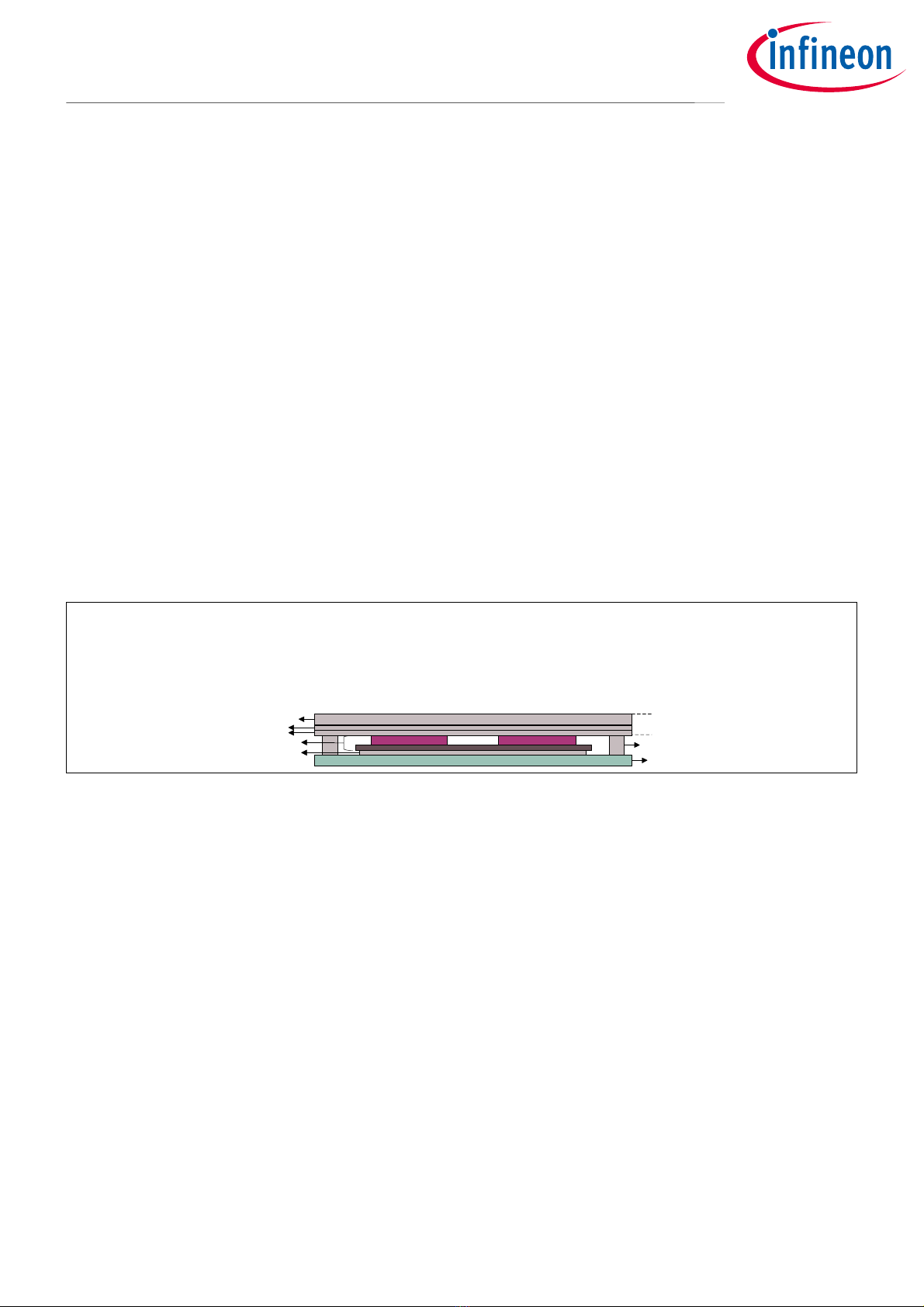
5. Transmitter coil assembly – The transmitter coil is MP-A2 type with specifications per Qi standards. The
coil is mounted on a separate coil PCB. A set of PCB shield (Shield PCB TOP and Shield PCB BOT) is mounted
on top of the coil and an acrylic sheet form the interface surface of the transmitter. The coil mounting
adhesive, spacers, and acrylic thickness are selected such that the distance between the coil top surface
and to interface surface is approximately 3.1 mm (Qi specification: 3 mm + 0.5 mm/-0.25 mm). See Figure 5
for coil assembly details.
.dz
PCB
Spacer
Acrylic
Coil assembly
Adhesive
PCB thickness – 1.6 mm
Acrylic thickness – 1.88 mm
Shield PCB Thickness – 0.6 mm Each
Spacer height – 4.8 mm
PCB + adhesive + Coil assembly – 4.9 mm
Dz gap – 3.08 mm
Shield PCB TOP
Shield PCB BOT
Figure 5 MP-A2 transmitter coil assembly
5. WLC1150-68LQXQ – The WLC1150 is a single controller unit to control the transmitter coil and USB PD
interface. The WLC1150 simplifies the transmitter board architecture with inbuilt gate drivers for the
auxiliary buck and inverter stage, inbuilt LDO for logic and core power, and more features. With an on-chip
32-bit Arm® Cortex®-M0 processor, 128-KB flash, 16-KB RAM, and 32-KB ROM, the firmware supporting the
complete high-power proprietary protocol and USB PD state machine logic can be programmed onto the
WLC1150 controller.
6. ASK demodulator – The ASK demodulator is based on coil voltage and bridge current. The demodulated
signal from both paths is processed through a dual opamp-based gain stage and a comparator and decoded
by the WLC1150 controller.
7. Q-factor and resonance frequency estimation – The Q-factor estimation from coil voltage is performed by
WLC1150 through the signal at Q_COMP. The coil voltage is processed through a blocking capacitor, voltage
divider, and clamping diode to feed to the WLC1150 controller for Q-factor and resonance frequency
estimation.
8. Status indication – The firmware indicates the various system states or events using the dual-color (red
and blue) status LED (LED1). See the Reference board operation to understand more details.

User guide 12 002-36393 Rev. *B
2023-02-06
WLC1150 MP-A2 50-W wireless power transmitter
(REF_WLC_TX50W_N1) user guide
WLC1150 wireless power transmitter system design
3.1.1 Board connectors
The transmitter board has power and signal connectors for operating and monitoring the wireless power
transfer. The function of each connector is listed in Figure 6.
Table 2 REF_WLC_TX50W_N1 board connectors
Connector Type Description
J1 Power USB Type-C connector for DC input through a USB-C power adaptor or
QC/AFC type AC/DC adaptor.*
This connector is also used to download configuration data/firmware
from the Wireless Configuration Utility through HPI dongle over the
Type-C CC lines. For more information, see section 4.2.1.
J3 Power Wire-to-board connector option for DC input through a variable DC power
supply *
J4 Power Jumper connection to power up the board either with USB PD or DC
power supply.
Jumper connection Pin 1-2 for PD adapter input.
Jumper connection Pin 2-3 for DC power supply.
J5 Signal Debug serial port. Connect to an HPI dongle (which is provided as part of
the reference board package) to view system status on PC using a
terminal emulator software (Tera Term, Putty, and so on). The data is
sent at a 1-M baud rate.
J2 Signal SWD connector. This connector is used to monitor, log, and dynamically
configure the firmware parameters from the Wireless Configuration
Utility through an HPI dongle over I2C lines. For more information, see
section 4.2.2.
J8 Power A J8 connector is needed to connect with the fan connector. This
connector is used to supply power to the fan.
L3 Power Terminals for transmitter coil connection.
* Do not power the transmitter board from both J1 and J3 simultaneously.
User guide 13 002-36393 Rev. *B
2023-02-06
WLC1150 MP-A2 50-W wireless power transmitter
(REF_WLC_TX50W_N1) user guide
WLC1150 wireless power transmitter system design
Figure 6 REF_WLC_TX50W_N1 power transmitter board power and signal connections
3.1.2 Test points
The test points in the REF_WLC_TX50W_N1 MP-A2 power transmitter board assist in monitoring and debugging
the wireless power transfer system. The list of test points and their functionality is covered in Table 3.
Table 3 List of test points on REF_WLC_TX50W_N1
Test point name Section Description
USB-IN Power Input power positive rail
USB-GND Power Input power ground rail
PVIN_0 Power – Buck/Inverter Input positive rail to buck converter and inverter
FAN_VDDD Power – Buck Buck stage output for Fan power supply
SW1_0 Power – Buck Buck stage switching node
HG1_0 Signal – Buck Buck stage high side MOSFET (Q3) gate signal
LG1_0 Signal – Buck Buck stage low side MOSFET (Q3) gate signal
VBB_1 Power – Inverter Input inverter power after the current sense resistor
COIL_SNS Power – Inverter Coil voltage; transmitter coil, and resonant capacitor
junction point
PWM_OUT Signal – Inverter Inverter stage PWM signal
PWM_IN1 Signal – Inverter PWM logic circuit O/P for inverter MOSFET Leg (Q4, Q5)

User guide 14 002-36393 Rev. *B
2023-02-06
WLC1150 MP-A2 50-W wireless power transmitter
(REF_WLC_TX50W_N1) user guide
WLC1150 wireless power transmitter system design
Test point name Section Description
PWM_IN2 Signal – Inverter PWM logic circuit O/P for inverter MOSFET Leg (Q6, Q7)
HG1_1 Signal – Inverter Inverter bank 1 high side MOSFET (Q4) gate signal
LG1_1 Signal – Inverter Inverter bank 1 low side MOSFET (Q5) gate signal
HG2_1 Signal – Inverter Inverter bank 2 high side MOSFET (Q6) gate signal
LG2_1 Signal – Inverter Inverter bank 2 high side MOSFET (Q7) gate signal
Q_COMP Signal – Q-factor Scaled coil voltage (for Q-factor measurement)
ASK_OUT Signal – ASK demodulator ASK demodulator output from WLC1150 to amplification
stage
OPAMP_GAIN Signal – ASK demodulator ASK demodulator gain stage amplifier output
CMP_REF Signal – ASK demodulator ASK demodulator comparator reference signal
OPAMP_CMP Signal – ASK demodulator ASK demodulator comparator output; digital signal to
WLC1150
VIN Power – WLC1150 Power input to WLC1150
VDDD Power – WLC1150 WLC1150 internal 5-V LDO output
VCCD Power – WLC1150 WLC1150 internal 1.8 V core LDO output
Q_COMP Signal – WLC1150 Signal used by WLC1150 for Q-factor estimation
GND1, GND2 Power Power side ground points
GND Signal Control side ground point
Note: For more information, see the reference board’s schematic in the REF_WLC_TX50W_N1 release
package.

User guide 15 002-36393 Rev. *B
2023-02-06
WLC1150 MP-A2 50-W wireless power transmitter
(REF_WLC_TX50W_N1) user guide
Reference board operation
4 Reference board operation
This section explains the procedure to operate the REF_WLC_TX50W_N1 reference board. It also explains the
procedure to configure the firmware in a static or dynamic manner and the procedure to download the
configuration or firmware onto the WLC1150-68LQXQ controller.
4.1 Wireless charging operation
The firmware supporting power transfer using USB PD input power is pre-programmed at the time of shipment.
The following procedure explains the steps required to do a power transfer using the USB PD input.
4.1.1 Wireless power transfer using Infineon high power protocol mode
(50W)
1. Ensure that a jumper shunt is placed at positions 1 and 2 of the power mode selection jumper (J4) of the Tx
reference board.
2. Connect the USB Type-C power adapter provided as part of the REF_WLC_TX50W_N1 package to the USB
Type-C connector (J1) of the Tx reference board.
3. Confirm that the status LED (LED1) blinks five times in blue and red. Now the board is ready for use.
Figure 7 Powering the WLC reference board
4. Place the Infineon 50-W Rx board on the Tx interface of the Tx reference board as shown in Figure 8.
5. Attach a load of up to 50W to the terminals of the Rx board. Ensure that the load is in the off state. The
status LED (LED1) of the Tx board glows blue when the power transfer is in progress.

User guide 16 002-36393 Rev. *B
2023-02-06
WLC1150 MP-A2 50-W wireless power transmitter
(REF_WLC_TX50W_N1) user guide
Reference board operation
Figure 8 Wireless power transfer using high power protocol
Note: Ensure that the DC load is connected to the Rx board as per the polarity marked on the Rx board.
6. Increase the load in the maximum step of 20 W to exceed 40 W. Observe that the fan located on the bottom
side of the Tx board turns on when the power transferred exceeds 40 W or when the Tx interface surface
temperature sensed by the thermistor on the Tx board exceed 45°C to cool the temperature of the Tx
interface surface.
7. During the power transfer the load on the Rx board can be varied up to 50-W. However, the maximum step
size for load change (application or removal) should not exceed 20-W.
8. Remove the Infineon Rx board from the Tx interface surface of the Tx reference board. Observe that the
status LED (LED1) turns off.
9. Disconnect the USB Type-C power adapter once the high-power transfer operation is complete.
Note: Avoid short circuits of the output load terminal of the Rx board. This may result in damage to the
Rx board.
4.1.2 Wireless power transfer using Qi protocol
The following procedure explains the steps to charging using the Qi protocol.
1. Repeat steps 1 to 3 of section 4.1.1 to exercise the power up the transmitter board.
2. Place the Qi phone/receiver on the Tx interface surface of the Tx reference board as shown in Figure 9.
3. The status LED (LED1) of the Tx board glows blue when the power transfer is in progress.
4. Observe that the status LED turns OFF when the phone/receiver is removed from the Tx interface surface or
once the phone is fully charged (100%).
5. Disconnect the USB Type-C power adapter once the power transfer operation is complete.
Note: The status LED continues to glow blue if the phone remains in trickle charging mode after the
battery is fully charged.
User guide 17 002-36393 Rev. *B
2023-02-06
WLC1150 MP-A2 50-W wireless power transmitter
(REF_WLC_TX50W_N1) user guide
Reference board operation
Figure 9 Powering the WLC reference board for Qi Rx/Phone
4.1.3 System Status and Status LED indication
Table 4 describes the status LED indications for various system states.
Table 4 System states and status LED indications
Note: The REF_WLC_TX50W_N1 reference board with factory default firmware may exhibit timeout-
bound retry of Qi power contract under extremely noisy ASK modulated signal conditions with a
few phones/receivers. Such behavior does not affect wireless charging performance. See the
REF_WLC_TX50W_N1 reference board’s test report for more details about the phone charging
cycle, ASK demodulation, and Qi 1.3.2 compliance test results. Download this report from the
REF_WLC_TX50W_N1 reference board webpage [1].
System state Status LED indication
Idle state No LED indication
Digital ping phase Blinks blue
Power delivery in progress Glows blue
Power Delivery/charge complete No LED indication
Foreign object (FO) detected Glows red until FO is removed
Fault during power transfer Blinks red until the fault is cleared
Abrupt end of power transfer (EPT) initiated by the
receiver
Blinks red

User guide 18 002-36393 Rev. *B
2023-02-06
WLC1150 MP-A2 50-W wireless power transmitter
(REF_WLC_TX50W_N1) user guide
Reference board operation
4.1.4 Troubleshooting
See Table 5 for troubleshooting the potential issues faced while operating the WLC 50 W Tx reference board.
Table 5 Troubleshooting of the WLC 50W Tx reference board operation
# Issue Possible cause Fix
1 The power transfer between
the transmitter and receiver
stops soon after it begins and
the status LED (LED1) glows
red.
There might be a foreign
object (FO) present on the
interface surface
Remove the receiver from the interface
surface and verify for any FO presence
and retry placing the receiver on the
interface surface.
2 The receiver reference board
REF_WLC_RX50W_N1 does
not provide output power
and debug logs show EPT121.
The receiver has
terminated the power
transfer because of a
potential fault in the
receiver
Power recycle the transmitter and retry.
In case the issue persists, contact
Infineon technical support.
3 The phone is not charging
when placed on the interface
surface of the WLC reference
board.
The phone may not be a
Qi-compliant phone.
Check with the phone manufacturer on
Qi compatibility. Get a Qi-compliant
phone.
4 The phone is charging at a
slow rate.
The phone may not
support Qi EPP capability.
Check with the phone manufacturer on
support for EPP capability. Get a phone
which can support EPP to charge at
15 W.
Note: By default, the REF_WLC_TX50W_N1 reference board is loaded with firmware that supports
USB PD-based power input. However, the reference board can be used for wireless power transfer
with high power protocol (50 W) using a DC supply, requiring a different firmware. See Appendix A
to understand the procedure for Wireless power transfer by using High power protocol (50 W)
mode with a DC input power supply.
User guide 19 002-36393 Rev. *B
2023-02-06
WLC1150 MP-A2 50-W wireless power transmitter
(REF_WLC_TX50W_N1) user guide
Reference board operation
4.2 Firmware download, configuration (static/dynamic), and
monitoring/debugging
WLC1150 IC is a programmable controller, which supports downloading the updated/modified configuration
data and downloading the firmware. It also supports monitoring the firmware parameters and dynamic tuning
of the firmware parameters. The WLC1150 controller supports these features through CC and/or I2C interfaces
based on the input power type supported in the current firmware, which is stored in the flash. See Table 6 to
understand the communication interface (CC/I2C) to use based on the current firmware type.
Table 6 Communication interface (CC/I2C) to use for firmware download and configuration
Scenario # Input power type
supported by the current
firmware stored in flash
Communication
interface for
downloading firmware/
configuration data
Communication interface for
monitoring firmware parameters
and dynamically configuring them
1 USB PD CC /I2C I2C
2 DC I2C
4.2.1 USB CC communication-based set-up
Figure 10 describes the set-up to download configuration data or firmware over the USB CC interface of the
WLC1150 controller.
Figure 10 USB CC communication-based setup
Execute the following procedure to create the setup:
1. Ensure that a jumper shunt is placed at positions 1 and 2 of the power mode selection jumper (J4) of the Tx
reference board.
2. Connect the HPI dongle to the Tx reference board using the USB Type-C cable.
3. Connect the HPI dongle to the PC using a USB micro-B cable.
4. The Power LED (LED1) on the HPI dongle glows blue, and the status LED (LED1) on the WLC1150 reference
board blinks in blue and red five times.
5. Open the Wireless Charging Configuration Utility from the Start menu in Windows.
6. Confirm that the reference board is selected under the Device Selection tab, as shown in Figure 11.

User guide 20 002-36393 Rev. *B
2023-02-06
WLC1150 MP-A2 50-W wireless power transmitter
(REF_WLC_TX50W_N1) user guide
Reference board operation
Figure 11 Selecting WLC1150 device in Wireless Charging Configuration Utility
7. Go to Tools > Firmware Update or select the Firmware Update option from the Home panel. Specify the
path for the firmware as shown in Figure 12 and click Program.
Figure 12 Selecting firmware for download
Table of contents
Other Infineon Transmitter manuals


