ISSI IS31FL3745 User manual

18×8 DOTS MATRIX LED DRIVER EVALUATION BOARD GUIDE
Integrated Silicon Solution, Inc. – ams.issi.com 1
Rev. A, 03/11/2019
DESCRIPTION
The IS31FL3745 is a general purpose 18×n (n=1~8)
LED Matrix programmed via 1MHz I2C compatible
interface. Each LED can be dimmed individually with
8-bit PWM data and 8-bit DC scaling data which
allowing 256 steps of linear PWM dimming and 256
steps of DC current adjustable level.
Additionally each LED open and short state can be
detected, IS31FL3745 store the open or short
information in Open-Short Registers. The Open-Short
Registers allowing MCU to read out via I2C compatible
interface. Inform MCU whether there are LEDs open or
short and the locations of open or short LEDs.
FEATURES
Supply voltage range: 2.7V to 5.5V
18 Current sink (Maximum)
Support 18 × n (n=1~8) LED matrix configurations
Individual 256 PWM control steps
Individual 256 DC current steps
Global 256 current setting
SDB rising edge reset I2C module
Programmable H/L logic:1.4/0.4, 2.4/0.6
29kHz PWM frequency
State lookup registers
Individual open and short error detect function
180 degree phase delay operation to reduce power
noise
De-Ghost
Cascade for synchronization of chips
QUICK START
Figure 1: Photo of IS31FL3745-CLS4 Evaluation Board
RECOMMENDED EQUIPMENT
5.0V, 2A power supply
ABSOLUTE MAXIMUM RATINGS
≤ 5.5V power supply
Caution: Do not exceed the conditions listed above, otherwise
the board will be damaged.
PROCEDURE
The IS31FL3745 evaluation board is fully assembled
and tested. Follow the steps listed below to verify
board operation.
Caution: Do not turn on the power supply until all connections
are completed.
1) Short JP1 (OPEN=EXT CTRL) to enable the
control of on board MCU (default status).
2) Connect the 5V DC power to VCC / GND in CON4,
or plug in the USB power input to micro-USB
(CON5).
3) Turn on the power supply, pay attention to the
supply current. If the current exceeds 1A, please
check for circuit fault.
EVALUATION BOARD OPERATION
The IS31FL3745 evaluation board has six display
modes. Press MODE button to switch configurations.
1) (Default mode) Rainbow #1.
2) Rainbow #2.
3) Purple breath.
4) Change colors.
5) White.
Note: IS31FL3745 solely controls the FxLED function on the
evaluation board.
ORDERING INFORMATION
Part No. Temperature Range Package
IS31FL3745-CLS4-EB -40°C to +125°C (Industrial) WLCSP-36, Lead-free
Table 1: Ordering Information
For pricing, delivery, and ordering information, please contacts ISSI’s analog marketing team at
analog@issi.com or (408) 969-6600

18×8 DOTS MATRIX LED DRIVER EVALUATION BOARD GUIDE
Integrated Silicon Solution, Inc. – ams.issi.com 2
Rev. A, 03/11/2019
SOFTWARE SUPPORT
EXT CTRL (JP1) default setting is close circuit. If it is
set to open, the on-board MCU will configure the I2C
pins and SDB pin to High Impedance and sleep.
External I2C and SDB signals can be connected to
TP4 to control the IS31FL3745 LED driver.
GND
SDA
SCL
SDB
VCC
Figure 2: Photo of Arduino UNO connected to Evaluation
Board
The steps listed below are an example using the
Arduino for external control.
The Arduino hardware consists of an Atmel
microcontroller with a bootloader allowing quick
firmware updates. First download the latest Arduino
Integrated Development Environment IDE (1.6.12 or
greater) from www.arduino.cc/en/Main/Software. Also
download the Wire.h library from
www.arduino.cc/en/reference/wire and verify that
pgmspace.h is in the directory …program
Files(x86)/Arduino/hardware/tools/avr/avr/include/avr
/. Then download the latest IS31FL3745 test firmware
(sketch) from the ISSI website
http://ams.issi.com/US/product-analog-fxled-driver.shtml.
1) Open EXT CTRL (JP1).
2) Connect the 5 pins from Arduino board to
IS31FL3745 EVB:
a) Arduino 5V pin to IS31FL3745 EVB VCC.
b) Arduino GND to IS31FL3745 EVB GND.
c) Arduino SDA (A4) to IS31FL3745 EVB SDA.
d) Arduino SCL (A5) to IS31FL3745 EVB SCL.
e) If Arduino use 3.3V MCU VCC, connect
3.3V to IS31FL3745 EVB SDB, if Arduino
use 5.0V MCU VCC, connect 5.0V or 3.3V
to EVB SDB.
(Arduino UNO MCU VCC is 5V, so SDB can
be 5V or 3.3V)
3) Use the test code in appendix Ⅰ or download the
test firmware (sketch) from the ISSI website,
a .txt file and copy the code to Arduino IDE,
compile and upload to Arduino.
4) Run the Arduino code for desired mode setting by
Arduino code.
Please refer to the datasheet to get more information about
IS31FL3745.

18×8 DOTS MATRIX LED DRIVER EVALUATION BOARD GUIDE
Integrated Silicon Solution, Inc. – ams.issi.com 3
Rev. A, 03/11/2019
GND
3V
SDA
SCL
INTB
USB_DM2
USB_DP2
DIO
GND
3V
GND
VIN
1
GND
2
EN
3
BP 4
VOUT 5
U2
LDO
3V
CLK
3V
MCU
3V Power
GND
GND
3V
DIO
SYNC
SCL
AD1
PVCC
3V
SDB
Micro USB
VCC
1
USB_DM
2
USB_DP
3
NC
4
GND
5
Con5
PVCC
USB_DM2
USB_DP2
3V
USB_DM
USB_DP
D1
DFL240
D2
DFL240
IO
PVCC
SDA
SCL
SDB
AD1
3V
PVCC
SW08
SW07
SW06
SW05
SW04
SW03
CS01
CS02
CS03
CS04
CS05
CS06
CS07
CS08
CS09
CS10
CS11
CS12
CS13
CS14
CS15
CS16
CS17
CS18
GND
PVCC
PVCC
PVCC
GND
SDB
OSCI
OSCO
PVCC
VBAT
1
PC13-ANTI_TAMP
2
PC14-OSC32_IN
3
PC15-OSC32_OUT
4
OSC_IN
5
OSC_OUT
6
NRST
7
VSSA
8
VDDA
9
PA0-WKUP/ADC_IN0/TIM2_CH1_ETR
10
PA1/ADC_IN1/TIM2_CH2
11
PA2/USART2_TX/ADC_IN2/TIM2_CH3
12
PA3/USART2_RX/ADC_IN3/TIM2_CH4
13
PA4/SPI1_NSS/ADC_IN4
14
PA5/SPI1_SCK/ADC_IN5
15
PA6/SPI1_MISO/ADC_IN6/TIM3_CH1
16
PA7/SPI1_MOSI/ADC_IN7/TIM3_CH2
17
PB0/ADC_IN8/TIM3_CH3
18
PB1/ADC_IN9/TIM3_CH4
19
PB2/BOOT1
20
PB10/I2C2_SCL/USART3_TX
21
PB11/I2C2_SDA/USART3_RX
22
VSS_1
23
VDD_1
24 PB12/SPI2_NSS/TIM1_BKIN 25
PB13/SPI2_SCK/TIM1_CH1N 26
PB14/SPI2_MISO/TIM1_CH2N 27
PB15/SPI2_MOSI/TIM1_CH3N 28
PA8/TIM1_CH1/MCO 29
PA9/USART1_TX/TIM1_CH2 30
PA10/USART1_RX/TIM1_CH3 31
PA11/CANRX/USBDM/ TIM1_CH4 32
PA12/CANTX/USBDP/TIM1_ETR 33
PA13/JTMS/SWDIO 34
VSS_2 35
VDD_2 36
PA14/JTCK/SWCLK 37
PA15/JTDI 38
PB3/JTDO 39
PB4/JNTRST 40
PB5 41
PB6/I2C1_SCL/TIM4_CH1 42
PB7/I2C1_SDA/TIM4_CH2 43
BOOT0 44
PB8/TIM4_CH3 45
PB9/TIM4_CH4 46
VSS_3 47
VDD_3 48
U3
STM32F103C8T6
SINK01
SINK02
SINK03
SINK04
SINK05
SINK06
SINK07
SINK08
SINK09
SINK10
SINK11
SINK12
SINK13
SINK14
SINK15
SINK16
SINK17
SINK18
RSET
3V
SW01
SW02
SW03
SW04
SW05
SW06
SINK09
SINK10SINK11
SINK12SINK13
SINK14SINK15
SINK16SINK17
SINK18
SW02
SW01
SW07
SW08
PA0
MOSI
MISO
SCK
CS
OSCO
OSCI OSCO
2
OSCI 4
GND
1
GND 3
Y1 8M
GND
SDA
SCL
SDB
MISO
1SDB 2
MOSI
35V 4
SCK
5SCL 6
CS
7SDA 8
PA0
9GND 10
TP4
PVCC
MISO
MOSI
SCK
CS
PA0
SINK01
SINK02SINK03
SINK04SINK05
SINK06SINK07
SINK08
1 2
3 4
5 6
7 8
9 10
11 12
13 14
15 16
CON1
C1
100nF
C2
100nF
C3
33p
C4
33p
C5
1μF
C6
1μF C7
10nF
C8
1μF
C9A
10μF
R1 4.7K
R2 4.7K
R4
100K
R5
10K
R6
100K
CS01 20R
R3
100K
AD2
PVCC
SDA
AD2
PVCC
1
2
JP1
GND
PA0
R9 1K
R8 100K 3V
R10
10K
R11 22R
R12 22R
R13
1.5K
1 2
3 4
5 6
7 8
9 10
11 12
13 14
15 16
CON2
1 2
3 4
5 6
7 8
9 10
11 12
13 14
15 16
CON3
SYNC
CS02
CS03
CS04
CS05
CS06
CS07
CS08
CS09
CS10
CS11
CS12
CS13
CS14
CS15
CS16
CS17
CS18
CS01
CLK
1
2
3
4
5
6
7
8
9
10
11
12
13
14
15
16
17
18
19
CON4
CS02 20R
CS03 20R
CS04 20R
CS05 20R
CS06 20R
CS07 20R
CS08 20R
CS09 20R
CS10 20R
CS11 20R
CS12 20R
CS13 20R
CS14 20R
CS15 20R
CS16 20R
CS17 20R
CS18 20R
PVCC
A3
VDD
F5
SDA
D3
SCL
E3
SDB
E5
RSET
F3
AD1
D4
AD2
E4
SYNC
F2
GND
F4
CS1 B2
CS2 B3
CS3 C3
CS4 C2
CS5 D2
CS6 D1
CS7 E2
CS8 E1
CS9 F1
CS10 F6
CS11 E6
CS12 D5
CS13 D6
CS14 C4
CS15 C6
CS16 C5
CS17 B4
CS18 B5
SW1 A2
SW2 A4
SW3 A1
SW4 A5
SW5 B1
SW6 A6
SW7 C1
SW8 B6
U1
31FL3745
K1
C9B
10μF
*Note1
Figure 3: IS31FL3745 Application Schematic
D37
RGB4P
D43
RGB4P
D38
RGB4P
D44
RGB4P
SW1 SW2 SW3 SW4 SW5 SW6
CS1
CS2
CS3
CS4
CS5
CS6
CS7
CS8
CS9
CS10
CS11
CS12
CS13
CS14
CS15
CS16
CS17
CS18
D39
RGB4P
D45
RGB4P
D40
RGB4P
D46
RGB4P
D41
RGB4P
D47
RGB4P
D6
RGB4P
D12
RGB4P
D18
RGB4P
D24
RGB4P
D30
RGB4P
D36
RGB4P
D5
RGB4P
D11
RGB4P
D17
RGB4P
D23
RGB4P
D29
RGB4P
D35
RGB4P
D4
RGB4P
D10
RGB4P
D16
RGB4P
D22
RGB4P
D28
RGB4P
D34
RGB4P
D3
RGB4P
D9
RGB4P
D15
RGB4P
D21
RGB4P
D27
RGB4P
D33
RGB4P
D2
RGB4P
D8
RGB4P
D14
RGB4P
D20
RGB4P
D26
RGB4P
D32
RGB4P
D1
RGB4P
D7
RGB4P
D13
RGB4P
D19
RGB4P
D25
RGB4P
D31
RGB4P
SW1
SW2
SW3
SW4
SW5
SW6
CS1
CS2 CS3
CS4 CS5
CS6 CS7
CS8 CS9
CS10 CS11
CS12 CS13
CS14 CS15
CS16 CS17
CS18
1 2
3 4
5 6
7 8
9 10
11 12
13 14
15 16
P1
Header 8X2
1 2
3 4
5 6
7 8
9 10
11 12
13 14
15 16
P2
Header 8X2
1 2
3 4
5 6
7 8
9 10
11 12
13 14
15 16
P3
Header 8X2
SW7
SW8
SW9
SW10
SW11
D42
RGB4P
D48
RGB4P
SW7 SW8
Figure 4: FxLED_6x8_ARRAY Schematic

18×8 DOTS MATRIX LED DRIVER EVALUATION BOARD GUIDE
Integrated Silicon Solution, Inc. – ams.issi.com 4
Rev. A, 03/11/2019
BILL OF MATERIALS
IS31FL3745
Name Symbol Description Qty Supplier Part No.
LED Driver U1 Matrix LED Driver 1 ISSI IS31FL3745
LDO U2 3.0V LDO 1 SGMICRO SGM2019-3.0YN5G
MCU U3 Microcontroller 1 STM STM32F103C8T6
Crystal Y1 Crystal, 8MHz 1 HLX HC-49S
Diode D1,D2 Diode, SMD 2 DIODES DFLS240
Resistor
CS01,CS02,
CS04,CS05,
CS07,CS08,
CS10,CS11,
CS13,CS14,
CS16,CS17
RES,20R,1/10W,±5%,SMD 12 Yageo RC0603JR-0720RL
Resistor
CS03,CS06,
CS09,CS12,
CS15,CS18
RES,20R,1/10W,±5%,SMD
(Note 1) 6 Yageo RC0603JR-0720RL
Resistor R1,R2 RES,4.7k,1/10W,±5%,SMD 2 Yageo RC0603JR-074K7L
Resistor R3,R4,R6,R8
RES,100k,1/10W,±5%,SMD 4 Yageo RC0603JR-07100KL
Resistor R5,R10 RES,10k,1/10W,±5%,SMD 2 Yageo RC0603JR-0710KL
Resistor R9 RES,1k,1/10W,±5%,SMD 1 Yageo RC0603JR-071KL
Resistor R11, R12 RES,22R,1/10W,±5%,SMD 2 Yageo RC0603JR-0722RL
Resistor R13 RES,1.5k,1/10W,±5%,SMD 1 Yageo RC0603JR-071K5L
Capacitor C1,C2 CAP,100nF,16V,±20%,SMD 2 Yageo CC0603MRX7R7BB104
Capacitor C3,C4 CAP,33pF,50V,±5%,SMD 2 Yageo CQ0603JRNPO9BN360
Capacitor C5,C6,C8 CAP, 1µF,16V,±10%,SMD 1 Yageo CC0603KRX7R7BB105
Capacitor C7 CAP,10nF,16V,±10%,SMD 1 Yageo CC0603KPX7R7BB103
Capacitor C9A,C9B CAP,10µF,16V,±20%,SMD 2 Yageo CC0805KKX7R7BB106
Button K1 Button SMD 1
Bill of Materials, refer to Figure 3 above.
FxLED 6x11 ARRAY
Name Symbol Description Qty
Supplier Part No.
Diode D1~D48 RGB LED, SMD 48 Everlight 9-237/R6GHBHC-A01/2T
Bill of Materials, refer to Figure 4 above.
Note 1: The value of these resistors on the evaluation board is 20Ω. For PVCC=5V and red LED application, prefer 51Ω for these resistors as
shown in datasheet Figure 1.

18×8 DOTS MATRIX LED DRIVER EVALUATION BOARD GUIDE
Integrated Silicon Solution, Inc. – ams.issi.com 5
Rev. A, 03/11/2019
0
00
0
123456789101112131415161719 18
1
2
4
3
2 4 6 8 10 12
1 3 5 7 9 11 13
14
15
16
24681012
135791113
14
15
16
1
1
0
0
0
0
2 4 6 8 10 12
1 3 5 7 9 11 13
14
15
16
2 1
8
6
4
2
10
1
3
5
7
9
Figure 4: Board Component Placement Guide - Top Layer
0
00
0
123456789101112131415161719 18
1
2
4
3
2 4 6 8 10 12
1 3 5 7 9 11 13
14
15
16
24681012
135791113
14
15
16
1
1
0
0
0
0
2 4 6 8 10 12
1 3 5 7 9 11 13
14
15
16
2 1
8
6
4
2
10
1
3
5
7
9
12
Figure 5: Board PCB Layout - Top Layer

18×8 DOTS MATRIX LED DRIVER EVALUATION BOARD GUIDE
Integrated Silicon Solution, Inc. – ams.issi.com 6
Rev. A, 03/11/2019
0
00
0
123456789101112131415161719 18
1
2
4
3
2 4 6 8 10 12
1 3 5 7 9 11 13
14
15
16
24681012
13579111 3
14
15
16
1
1
0
0
0
0
2 4 6 8 1 0 12
1 3 5 7 9 11 13
14
15
16
2 1
8
6
4
2
10
1
3
5
7
9
Figure 6: Board Component Placement Guide - Bottom Layer
0
00
0
123456789101112131415161719 18
12
1
2
4
3
1 2
1
2
1
2
1
2
1 2
1
21
2
1
2
1
2
1 2
1
2
1
2
1
2
2 4 6 8 10 12
1 3 5 7 9 11 13
14
15
16
1
2
1
2
12
1
2
1 2
1
2
24681012
135791 113
14
15
16
1
1
0
0
0
0
2 4 6 8 10 12
1 3 5 7 9 11 13
14
15
16
34
21
1
2
1
2
1
2
1
2
1
2
1
2
1
2
1
2
1
2
1
2
1
2
1
2
1
2
1
2
1
2
1
2
1
2
1
2
2 1
8
6
4
2
10
1
3
5
7
9
1
2
1
2
1 2
Figure 7: Board PCB Layout - Bottom Layer

18×8 DOTS MATRIX LED DRIVER EVALUATION BOARD GUIDE
Integrated Silicon Solution, Inc. – ams.issi.com 7
Rev. A, 03/11/2019
Figure 8: Board Component Placement Guide - Top Layer
23
14
23
14
23
14
23
14
23
14
23
14
23
14
23
14
23
14
23
14
23
14
23
14
23
14
23
14
23
14
23
14
23
14
23
14
23
14
23
14
23
14
23
14
23
14
23
14
23
14
23
14
23
14
23
14
23
14
23
14
23
14
23
14
23
14
23
14
23
14
23
14
23
14
23
14
23
14
23
14
23
14
23
14
23
14
23
14
23
14
23
14
23
14
23
14
Figure 9: Board PCB Layout - Top Layer

18×8 DOTS MATRIX LED DRIVER EVALUATION BOARD GUIDE
Integrated Silicon Solution, Inc. – ams.issi.com 8
Rev. A, 03/11/2019
Figure 10: Board Component Placement Guide - Bottom Layer
1513119753
2 4 6 8 10 12 14 16
1 15131 19753
2 4 6 8 10 12 14 16
1
1
16 14 12 10 8 6 4 2
3579111 31 5
Figure 11: Board PCB Layout - Bottom Layer
Copyright © 2019
Integrated Silicon Solution, Inc. All rights reserved. ISSI reserves the right to make changes to this specification and its
products at any
time without notice. ISSI assumes no liability arising out of the application or use of any information, products or services described herein. Customers are
advised to obtain the latest version of this device specification before relying on any published information and before placing orders for products.
Integrated Silicon Solution, Inc. does not recommend the use of any of its products in life support applications where the failure or malfunction of the
product can reasonably be expected to cause failure of the life support system or to significantly affect its safety or effectiveness. Products are not
authorized for use in such applications unless Integrated Silicon Solution, Inc. receives written assurance to its satisfaction, that:
a.) the risk of injury or damage has been minimized;
b.) the user assume all such risks; and
c.) potential liability of Integrated Silicon Solution, Inc is adequately protected under the circumstances

18×8 DOTS MATRIX LED DRIVER EVALUATION BOARD GUIDE
Integrated Silicon Solution, Inc. – ams.issi.com 9
Rev. A, 03/11/2019
REVISION HISTORY
Revision Detail Information Data
A Initial Release 2019.03.11

18×8 DOTS MATRIX LED DRIVER EVALUATION BOARD GUIDE
Integrated Silicon Solution, Inc. – ams.issi.com 10
Rev. A, 03/11/2019
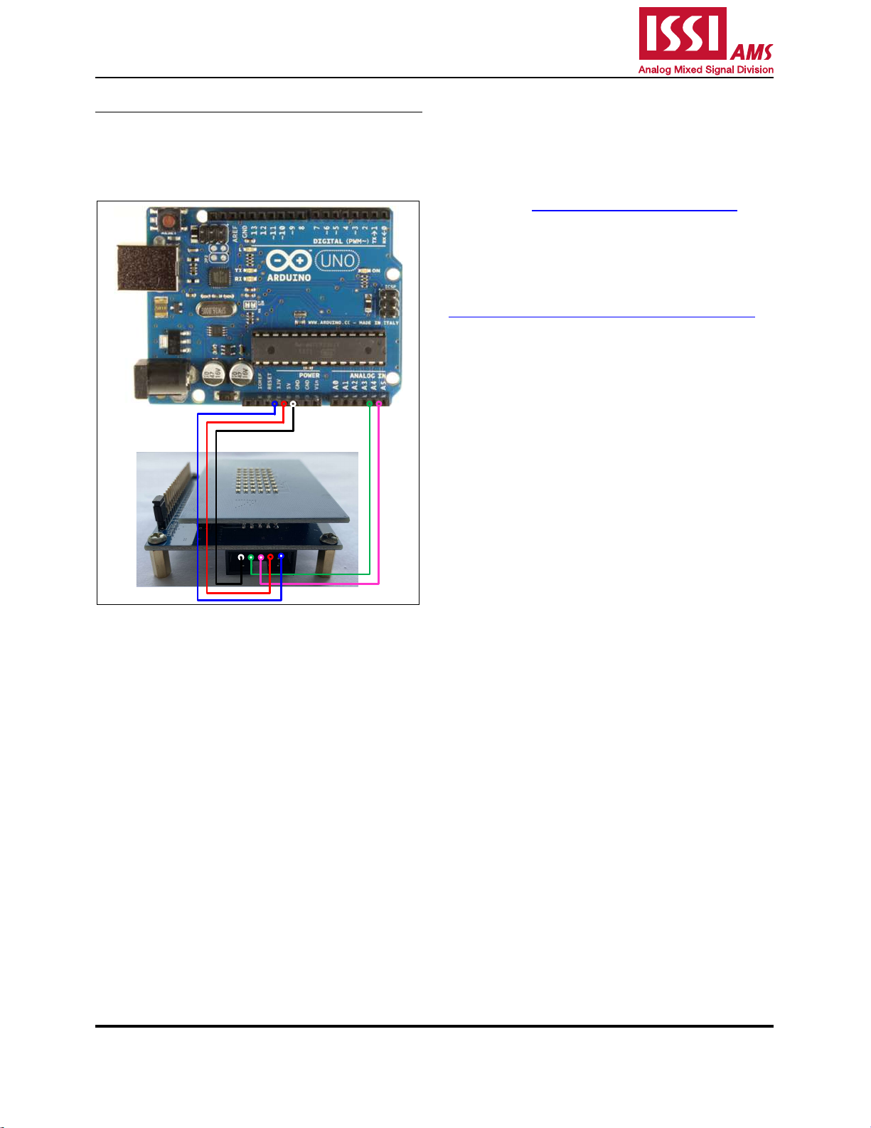
APPENDIX Ⅰ: IS31FL3745 Arduino Test Code V01A
#include<Wire.h>
#include<avr/pgmspace.h>
#define Addr_GND_GND 0x40
void setup() {
// put your setup code here, to run once:
pinMode(13, OUTPUT);//ARDUINO BOARD LED control
Wire.begin();
Wire.setClock(400000);//I2C 400kHz
}
byte PWM_Gamma64[64]=
{
0x00,0x01,0x02,0x03,0x04,0x05,0x06,0x07,
0x08,0x09,0x0b,0x0d,0x0f,0x11,0x13,0x16,
0x1a,0x1c,0x1d,0x1f,0x22,0x25,0x28,0x2e,
0x34,0x38,0x3c,0x40,0x44,0x48,0x4b,0x4f,
0x55,0x5a,0x5f,0x64,0x69,0x6d,0x72,0x77,
0x7d,0x80,0x88,0x8d,0x94,0x9a,0xa0,0xa7,
0xac,0xb0,0xb9,0xbf,0xc6,0xcb,0xcf,0xd6,
0xe1,0xe9,0xed,0xf1,0xf6,0xfa,0xfe,0xff
};
void IS_IIC_WriteByte(uint8_t Dev_Add,uint8_t Reg_Add,uint8_t Reg_Dat)//writing an LED register
{
Wire.beginTransmission(Dev_Add/2);
Wire.write(Reg_Add); // sends regaddress
Wire.write(Reg_Dat); // sends regaddress
Wire.endTransmission(); // stop transmitting
}
void loop() {
// put your main code here, to run repeatedly:
mainloop();
}
void Init3745(void)
{
int i,j;
IS_IIC_WriteByte(Addr_GND_GND,0xfe,0xc5);
IS_IIC_WriteByte(Addr_GND_GND,0xfd,0x00);//page 0
for(i=0;i<0x91;i++)
{
IS_IIC_WriteByte(Addr_GND_GND,i,0);//PWM
}
IS_IIC_WriteByte(Addr_GND_GND,0xfe,0xc5);
IS_IIC_WriteByte(Addr_GND_GND,0xfd,0x01);//page 1
for(i=1;i<0x91;i++)
{
IS_IIC_WriteByte(Addr_GND_GND,i,0xff);//scaling
}
IS_IIC_WriteByte(Addr_GND_GND,0xfe,0xc5);
IS_IIC_WriteByte(Addr_GND_GND,0xfd,0x02);//page 2
IS_IIC_WriteByte(Addr_GND_GND,0x02,0x70);
IS_IIC_WriteByte(Addr_GND_GND,0x01,0xFF);//GCC
IS_IIC_WriteByte(Addr_GND_GND,0x00,0x01);//
}
void mainloop(void)//
{
int i,j;
Init3745();
digitalWrite(13, LOW); // turn the ARDUINO BOARD LED on (HIGH is the voltage level)
while(1)
{
//BLUE
digitalWrite(13, HIGH); // turn the ARDUINO BOARD LED on (HIGH is the voltage level)
IS_IIC_WriteByte(Addr_GND_GND,0xfe,0xc5);
IS_IIC_WriteByte(Addr_GND_GND,0xfd,0x00);//page 0

18×8 DOTS MATRIX LED DRIVER EVALUATION BOARD GUIDE
Integrated Silicon Solution, Inc. – ams.issi.com 11
Rev. A, 03/11/2019
for(j=0;j<64;j++)
{
for(i=1;i<0x91;i=i+3)
{
IS_IIC_WriteByte(Addr_GND_GND,i,PWM_Gamma64[j]);//PWM}
}
}
delay(500);
digitalWrite(13, LOW); // turn the ARDUINO BOARD LED OFF (HIGH is the voltage level)
IS_IIC_WriteByte(Addr_GND_GND,0xfe,0xc5);
IS_IIC_WriteByte(Addr_GND_GND,0xfd,0x00);//page 0
for(j=63;j>=0;j--)
{
for(i=1;i<0x91;i=i+3)
{
IS_IIC_WriteByte(Addr_GND_GND,i,PWM_Gamma64[j]);//PWM}
}
}
delay(500);
//GREEN
digitalWrite(13, HIGH); // turn the ARDUINO BOARD LED on (HIGH is the voltage level)
IS_IIC_WriteByte(Addr_GND_GND,0xfe,0xc5);
IS_IIC_WriteByte(Addr_GND_GND,0xfd,0x00);//page 0
for(j=0;j<64;j++)
{
for(i=2;i<0x91;i=i+3)
{
IS_IIC_WriteByte(Addr_GND_GND,i,PWM_Gamma64[j]);//PWM}
}
}
delay(500);
digitalWrite(13, LOW); // turn the ARDUINO BOARD LED OFF (HIGH is the voltage level)
IS_IIC_WriteByte(Addr_GND_GND,0xfe,0xc5);
IS_IIC_WriteByte(Addr_GND_GND,0xfd,0x00);//page 0
for(j=63;j>=0;j--)
{
for(i=2;i<0x91;i=i+3)
{
IS_IIC_WriteByte(Addr_GND_GND,i,PWM_Gamma64[j]);//PWM}
}
}
delay(500);
//RED
digitalWrite(13, HIGH); // turn the ARDUINO BOARD LED on (HIGH is the voltage level)
IS_IIC_WriteByte(Addr_GND_GND,0xfe,0xc5);
IS_IIC_WriteByte(Addr_GND_GND,0xfd,0x00);//page 0
for(j=0;j<64;j++)
{
for(i=3;i<0x91;i=i+3)
{
IS_IIC_WriteByte(Addr_GND_GND,i,PWM_Gamma64[j]);//PWM}
}
}
delay(500);
digitalWrite(13, LOW); // turn the ARDUINO BOARD LED OFF (HIGH is the voltage level)
IS_IIC_WriteByte(Addr_GND_GND,0xfe,0xc5);
IS_IIC_WriteByte(Addr_GND_GND,0xfd,0x00);//page 0
for(j=63;j>=0;j--)
{
for(i=3;i<0x91;i=i+3)
{
IS_IIC_WriteByte(Addr_GND_GND,i,PWM_Gamma64[j]);//PWM}
}
}
delay(500);
//WHITE
digitalWrite(13, HIGH); // turn the ARDUINO BOARD LED on (HIGH is the voltage level)
IS_IIC_WriteByte(Addr_GND_GND,0xfe,0xc5);

18×8 DOTS MATRIX LED DRIVER EVALUATION BOARD GUIDE
Integrated Silicon Solution, Inc. – ams.issi.com 12
Rev. A, 03/11/2019
IS_IIC_WriteByte(Addr_GND_GND,0xfd,0x00);//page 0
for(j=0;j<64;j++)
{
for(i=1;i<0x91;i++)
{
IS_IIC_WriteByte(Addr_GND_GND,i,PWM_Gamma64[j]);//PWM}
}
}
delay(500);
digitalWrite(13, LOW); // turn the ARDUINO BOARD LED OFF (HIGH is the voltage level)
IS_IIC_WriteByte(Addr_GND_GND,0xfe,0xc5);
IS_IIC_WriteByte(Addr_GND_GND,0xfd,0x00);//page 0
for(j=63;j>=0;j--)
{
for(i=1;i<0x91;i++)
{
IS_IIC_WriteByte(Addr_GND_GND,i,PWM_Gamma64[j]);//PWM}
}
}
delay(500);
}
}
Table of contents
Other ISSI Motherboard manuals

ISSI
ISSI LUMISSIL IS31SE5117 User manual

ISSI
ISSI IS31FL3238 User manual

ISSI
ISSI IS31AP4915 User manual

ISSI
ISSI IS32LT3120 User manual

ISSI
ISSI IS31LT3948 User manual

ISSI
ISSI Flicker-Free IS31LT3935 User manual

ISSI
ISSI IS31LT3135-V1 User manual

ISSI
ISSI IS31IO7325 User manual

ISSI
ISSI IS31LT3360 User manual

ISSI
ISSI IS31LT3918 User manual