Jaden DLB1-0D40S2G User manual

Table of Contents
1 Summary .............................................................................................. 3
1.1 Name plate ........................................................................................................ 3
1.2 Product series .................................................................................................... 4
1.3 Technical standards............................................................................................6
1.4 Peripheral Electrical Devices and System Configuration......................................8
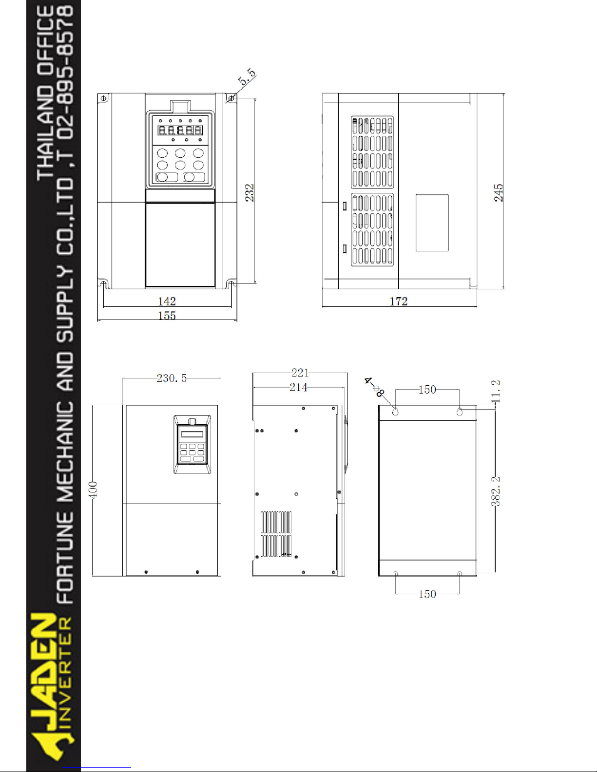
1.5 Product outline and installation dimensions.........................................................9
2 Wirings ............................................................................................... 14
2.1 Standard wiring diagrams................................................................................. 14
2.2 Main circuit wiring terminals ........................................................................... 16
2.3 Control circuit wiring terminals........................................................................ 17
3 Panel operations ................................................................................ 23
3.1 Keyboard interface........................................................................................... 23
3.2 Parameter setting example & motor auto-tuning................................................ 25
3.3 JOG................................................................................................................. 26
4 Function codes (Parameters) ............................................................ 27
4.1 Basic monitoring parameters: d0.00-d0.41........................................................ 27
4.2 Basic functions group: P0.00-P0.28.................................................................. 31
4.3 First motor parameters: P1.00-P1.37................................................................. 41
4.4 V/F control parameters: P2.00-P2.15................................................................ 46
4.5 Vector control parameters: P3.00-P3.22............................................................ 51
4.6 Input terminals: P4.00-P4.39............................................................................ 55
4.7 Output terminals: P5.00-P5.22.......................................................................... 68
4.8 Start/stop control: P6.00-P6.15......................................................................... 74
4.9 Operation panel and display: P7.00-P7.14......................................................... 79
4.10 Auxiliary functions: P8.00-P8.53.................................................................... 82
4.11 Fault and protection: P9.00-P9.70................................................................... 92
4.12 PID functions: PA.00-PA.28......................................................................... 103
4.13 Swing Frequency, Fixed Length and Count: PB.00-PB.09............................. 108
4.14 Multi-reference and simple PLC: PC.00-PC.51............................................. 111
4.15 Communication parameters: PD.00-PD.06.................................................... 116
4.16 PE group: reserved....................................................................................... 117
4.17 Function code management: PP.00-PP.04..................................................... 117
4.18 Torque control parameters: B0.00-B0.08....................................................... 119
4.19 Control optimization parameters: B5.00-B5.09.............................................. 121
4.20 Extended function parameters: B9.00-B9.09 ................................................. 123

2
5 Fault and solutions .......................................................................... 124
5.1 Fault and solutions......................................................................................... 124
5.2 Common fault and solutions........................................................................... 130
6 Repair and maintenance .................................................................. 132
6.1 Routine maintenance...................................................................................... 132
6.2 Replacement of vulnerable components.......................................................... 132
7 MODBUS communication protocol ................................................. 133
7.1 Communication protocol................................................................................ 133
7.2 Verification mode.......................................................................................... 136
7.3 Communication addresses.............................................................................. 137
Appendix I: Parameter list .................................................................. 141
Appendix II: Expansion cards ............................................................ 156
Appendix II-1Multi-function card DLB1-PC1 ...................................................... 156
Appendix II-2 Encoder card (PG card)................................................................. 158
Appendix III Brake accessories .......................................................... 162
Appendix IV: Selection of Peripheral Electrical Devices ................... 164
Appendix V: Guide for complying with EMC ..................................... 169
Appendix VI: Safety instructions ....................................................... 171

-
3
-
1 Summary
1.1 Name plate
Graph 1-1 Nameplate
Important:
Please read Appendix VI Safety Instructions carefully before and during using JADEN DLB1
inverters.

-
4
-
1.2 Product series
Inverter model Rated output
power(kW)Rated input current
(A) Rated output
current (A)
Single Phase input:AC 220V-15%~+10%, 50/60Hz
DLB1-0D40S2G 0.4 5.9 2.5
DLB1-0D75S2G 0.75 8.3 4
DLB1-01D5S2G 1.5 14.1 7
DLB1-02D2S2G 2.2 24.2 10
Three phase input:AC 380V-15%~+10%, 50/60Hz
DLB1-0D75T4G 0.75 4.3 2.5
DLB1-01D5T4G 1.5 5.2 3.7
DLB1-02D2T4G 2.2 6.0 5
DLB1-0004T4G 4.0 10.5 8.5
DLB1-05D5T4G 5.5 15.5 13
DLB1-07D5T4G 7.5 20.5 16
DLB1-0011T4G 11 27.6 25
DLB1-0015T4G 15 37.1 32
DLB1-0018T4G 18 41.9 38
DLB1-0022T4G 22 49.3 45
DLB1-0030T4G 30 65.7 60
DLB1-0037T4G 37 80.6 75
DLB1-0045T4G 45 96.4 90
DLB1-0055T4G 55 117.6 110
DLB1-0075T4G 75 166.4 150
DLB1-0090T4G 90 184.3 170
DLB1-0110T4G 110 226.8 210
DLB1-0132T4G 132 268.1 250
DLB1-0160T4G 160 321.1 300
DLB1-0187T4G 187 368.0 340
DLB1-0200T4G 200 406.6 380
DLB1-0220T4G 220 442.7 415
DLB1-0250T4G 250 503.0 470
DLB1-0280T4G 280 555.9 520
DLB1-0315T4G 315 650.7 600

-
5
-
DLB1-0355T4G 355 754.5 650
DLB1-0400T4G 400 797.6 725
Three phase input: AC 660V-15%~+10%, 50/60Hz
DLB1-0D75T7G 0.75 4.1 2.5
DLB1-01D5T7G 1.5 4.9 3.7
DLB1-02D2T7G 2.2 5.7 5
DLB1-0004T7G 4.0 9.4 8
DLB1-05D5T7G 5.5 12.5 11
DLB1-07D5T7G 7.5 18.3 15
DLB1-0011T7G 11 23.1 22
DLB1-0015T7G 15 29.8 27
DLB1-0018T7G 18 35.7 34
DLB1-0022T7G 22 41.7 40
DLB1-0030T7G 30 57.4 55
DLB1-0037T7G 37 66.5 65
DLB1-0045T7G 45 81.7 80
DLB1-0055T7G 55 101.9 100
DLB1-0075T7G 75 137.4 130
DLB1-0090T7G 93 151.8 147
DLB1-0110T7G 110 185.3 180
DLB1-0132T7G 132 220.7 216
DLB1-0160T7G 160 264.2 259
DLB1-0187T7G 187 309.4 300
DLB1-0200T7G 200 334.4 328
DLB1-0220T7G 220 363.9 358
DLB1-0250T7G 250 407.9 400
DLB1-0280T7G 280 457.4 449
DLB1-0315T7G 315 533.2 516
DLB1-0355T7G 355 623.3 570
DLB1-0400T7G 400 706.9 650

-
6
-
1.3 Technical standards
Specifications
Basic functions
Control system CurrentVector General Purpose Inverter.
Compatible motor
Induction motor and Synchronous motor.
Maximum
frequency Vector control:0~300Hz;
V/F control:0~3200Hz.
Wave-carrier
frequency 0.5kHz~16kHz;
Depending on load, can automatically adjust wave-carrier frequency.
Input frequency
resolution Digital setting:0.01Hz;
Analog setting:maximum frequency×0.025%.
control mode Open vector control(SVC);
Closed loop vector control(FVC);
V/F control.
Starting torque G type:0.5Hz/150%(SVC); 0Hz/180%(FVC).
P type:0.5Hz/100%.
Speed range 1:100(SVC) 1:1000(FVC)
Speed
stability
accuracy ±0.5%(SVC) ±0.02%(FVC)
Torque control
accuracy ±5%(FVC)
Overload capacity
G type:150%rated current60s; 180%rated current3s;
P type:120%rated current60s; 150%rated current3s.
Torque boost Automatic ormanual 0.1%~30.0%,
V/F curve
•
Straight-line V/F curve
•Multi-point V/F curve
•N-power V/F curve (1.2-power, 1.4-power, 1.6-power,
•1.8-power, 2-power square)
V/F separation Two types: complete separation; half separation. AVR output.
Ramp mode
•
Straight-line ramp
•S-curve ramp
Four groups of acceleration/deceleration time with the
range of 0.0–6500.0s
DC braking DC braking frequency: 0.00 Hz to maximum frequency
Braking time: 0.0–36.0s
Braking action current value: 0.0%–100.0%
JOG control JOG frequency range: 0.00–50.00 Hz
JOG acceleration/deceleration time: 0.0–6500.0s
Simple PLC Up to 16 speeds via the simple PLC function or combination of DI terminal
states
Onboard PID Process-controlled closed loop control system
Auto voltage
regulation (AVR) Keep constant output voltage automatically when grid voltage fluctuates.
Overvoltage/
Overcurrent stall
control
The current and voltage are limited automatically during the running process
so as to avoid frequent tripping due to overvoltage/overcurrent.
Fast current limit
function Protect inverter from overcurrent malfunctions.
Torque limit and
control
It can limit the torque automatically and prevent frequent over current tripping
during the running process. Torque control can be implemented in the FVC
mode.

-
7
-
Special Functions
Power dip ride
through The load feedback energy compensates the voltage reduction so that the
Invertercan continue to run for a short time.
Timing control Time range: 0.0–6500.0 minutes
Two-motor
switchover Two motors can be switched over via two groups of motor parameters.
Fieldbus Supports RS485, Profibus-DP, CANlink, CANopen (need extention cards)
Background
software Change inverter parameter & vitual oscillograph to monitor inverter status.
Operations
Command source
•Operation panel
•Control terminals
•Serial communication port
You can perform switchover between these sources invarious ways.
Frequencysource 11frequency sources, such as digital setting, analog voltage setting, analog
current setting, pulse setting and serial communication port setting. You can
perform switchover between these sources in various ways.
Auxiliary
frequency source 11auxiliary frequency sources. It can implement fine tuning of auxiliary
frequency and frequency synthesis.
Input terminal
6 digital input (DI) terminals, DI5 supports up to 100 kHz high-speed pulse
input;
3 analog input (AI) terminals, support 0–10 V voltageinput or 4–20 mA current
input
Output terminal
2 digital output (DO) terminal (FM supports 0–10 kHz square wave signal
output)
1 relay output terminal
2 analog output (AO) terminal that support 0–20 mA current output or 0–10 V
voltage.
Display and panel
LED display Displays parameters.
Key lock It can lock the keys partially or completely and define thefunction range of
some keys so as to prevent mis-function.
Protection
function
Motor short-circuit detection at power-on, input/output phase loss protection,
overcurrent protection, overvoltage protection, undervoltage protection,
overheat protection and overload protection
Optional parts PG card, brake unit, RS485 card, CAN card, Profibus-DP card
Environment
Location Indoor, free from direct sunlight, dust, corrosive gas, combustible gas, oil
smoke, vapour, drip or salt.
Altitude Lower than 1000m.
Ambient
temperature -10°C to +40°C (de-rated if the ambient temperature is between 40°C and
50°C)
Humidity Less than 95%RH, without condensing
Vibration Less than 5.9m/s2(0.6g).
Storage
temperature -20
℃
~+60
℃
.

-
8
-
1.4 Peripheral Electrical Devices and System Configuration
Grounding
Circuit
braker
Motor
DC reactor
EMC filter
Grounding
AC reactor
Inverter
EMC filter
Contactor
AC reactor
Power
Brake
resistor
Brake
unit
Graph 1-2 Peripheral electrical devices

-
9
-
1.5 Product outline and installation dimensions
1.5.1 Product outline& installation dimensions
Graph 1-3 0.4W~1.5KW product outlines & dimensions
Graph 1-42.2KW~3.7KW product outline & dimensions

-
10
-
Graph 1-5 5.5~7.5KW product outline & dimensions
Graph 1-611~18.5KW product outline & dimensions

-
11
-
Graph 1-722~30KW product outline & dimensions
Graph 1-837~55KW product outline & dimensions

-
12
-
Graph 1-875~110KW product outline & dimensions
Graph 1-9 132~160KW product outline & dimensions

-
13
-
1.5.2 Detachable keyboard(operation panel) dimensions
Graph 1-10 detachable keyboard outline dimensions
Graph 1-11 detachable keyboard aperture dimensions

-
14
-
2 Wirings
2.1 Standard wiring diagrams
Graph 2-8 0.4~18.5KW inverter wiring diagram

-
15
-
Graph 2-922~400KW inverter wiring diagram

-
16
-
2.2 Main circuit wiring terminals
0.4KW~15KW:
P+ P- PB R S T PE U V W
Terminal name
Function
R
,
S
,
T
Three phase power input terminal
P+
,
PB
External brake resistor
terminal
P
-
DC bus
negative
terminal
U
,
V
,
W
Three phase AC output terminal
PE
Grounding terminal
18.5KW~400KW:
Terminal name Function
R, S, T Three phase power input terminal
(+), (-) External brake unit terminal
P, (+) External DC reactor terminal
U, V, W Three phase AC output terminal
Grounding terminal
R S T (+) P (-) U V W
POWER MOTOR

-
17
-
2.3 Control circuit wiring terminals
2.3.1 Control circuit terminal definitions
GND
AO1
AO2
AI1 AI2 AI3
DI2 DI4 DI6
DO1
COM
TC1
GND
+10V
+24V
SP
COM
DI1 DI3
DI5
FM +24V
TA1
TB1
2.3.2 Control circuit signals
Category
Terminal Name Function Specifications
Input
Digital
DI1
Multi-function
input terminal
X1
Default setting: Forward
operation(FWD)
Optical coupler
insulation
DC24V/8mA
When using external
power supply,
voltage range: 9~
30V
DI5 can configure as
high speed pulse
input. pulse range:
0~100kHz.
DI2
Multi-function
input terminal
X2
Default setting: Forward
JOG(FJOG)
DI3
Multi-function
input terminal
X3
Default setting: Fault reset
(RESET)
DI4
Multi-function
input terminal
X4
Default setting: Multi-speed
terminal1
DI5
Multi-function
input terminal
X5
Default setting: Multi-speed
terminal12
DI6
Multi-function
input terminal
X6
Default setting: REV
operation(REV)
SP Multi-function
input common
Default: +24V short-circuit with SP
by jumper
Analog
10V
Analog
10V
Power
Output capacity: 10mA or below,
1kΩ~5kΩ
0~20mA input: input
impedance is 500
ohms.
0~10V input: input
impedance is 20K
ohms.
AI1
Analog
frequency setting
1
DC: 0~10V or 0~20mA
(resolution1/1000)
AI2
Analog
frequency setting
2
DC: 0~10V or 0~20mA
(resolution1/1000)
AGND Analog common 0V

-
18
-
Category
Terminal Name Function Specifications
terminal
Output
Relay
TA1 A node output Default setting: stop fault during
operation
TA1—TC1: normally open
TB1—TC1: normally close
Node capacity:
AC250V, 3A.
TB1 B node output
TZ1 Node output
common terminal
Digital
DO1
Open collector
output
1
Default setting: inverter in
operation
open collector output;
Optical-coupler
output capacity:
Below DC24V, 50mA.
FM
High speed pulse
output
Pulse range: 0~100kHz.
Open collector output.
Defined by P5.00: FM
terminal output mode
selection.
When used as high
speed pulse output,
maximum frequency
is 100kHz.
COM
FM output
common terminal
Analog
AO1 Analog monitor
output1
Voltage or current output;
Default setting:output frequency Output voltage range:
0~10V;
Output current range:
0~20mA.
AO2 Analogm monitor
output2
Voltage or current output;
Default setting: output frequency
AGND Analog common
terminal 0V
Power
+24V DC24V power
positive node Used with DI, DO
Output
capacity:below
200mA;
Default:
+24V short-circuit
with SP
COM
DC24V power
negative node

-
19
-
2.3.3Control circuitwiring notes
1. Analog input terminal
As analogy voltage signals can be easily affected by external interference,
shielded cables shall be used. Cables shall be as short as possible and not exceeding 20
meters. As shown in Graph 2-12 & 2-13, in some severe circumstances, filter
capacitor or ferrite bread shall be used in analog signal side.
PE
+10V
GND
AI1
DLB1
Potentiometer
Less than 20m
Graph 2-12Analog input terminal wiring
DLB1
AI1
GND
0.022uF
50V
Ferrite bread
External
analog
source
Graph 2-13Analog input terminaltreatment
2. Digital input terminal
Shielded cables shall be used. Cables shall be as short as possible and not
exceeding 20 meters. When using active drive mode, user shall take necessary filter
measures to counter power interference. It is recommended to use node control mode.
Digital inputs include NPN input and PNP input.
(a)NPN input:Most common. Use internal 24V power; +24V terminal
short-circuit with SP terminal; COM terminal is common;J9 is 23 jumper; also known
as drain wiring mode.

-
20
-
NPN
信号
COM
4.7K
4.7K
D15
D11
SP
+24V
0V
+24V
+VCC
3.3Ω
External
controller Inverter
Graph 2-14 NPN inputwirng
(b)PNP input:Use external 24V power; external power negative node is
connected withSP terminal; external terminal positive node is common; external
power voltage range is 9~30V; J9 is 12 jumper; also known as source wiring mode.
PNP信号
COM
4.7K
4.7K
D15
D11
SP
+24V
0V
+24V
+VCC
3.3Ω
External
controller Inverter
9-30V
Graph 2-15 PNP input wiring
3. Output terminal
Digital output is open collector output. When using external power, please
connect external power negative node to COM terminal. Maximumcurrent is 50mA for
open collector output. If external load is relay, please install fly-wheel diode to both ends
of the relay.
«Note:please install fly-wheel diode polars correctly, otherwise internal
components will be damaged.
This manual suits for next models
57
Table of contents