JBL JBLBARSBLKAM User manual

CONTENTS
2
4
15
16
Technical Specifications
Safety Instruction, Warning & Notes
Dismantling Instructions
Set Block Diagram
Set Wiring Diagram
Schematic & Layout Diagrams
Set Mechanical Exploded View
Spare Parts List
Revision List
23
24
25
Service Manual
Released by Global Quality SL harman/kardon, Inc. Ver. 1.2Mar.2019
8
JBL BAR STUDIOJBL BAR STUDI
O
14
S
O
SKU: JBLBARSBLKAM, JBLBARSBLKEP, JBLBARSBLKUK, JBLBARSBLKAS, JBLBARSBLKCN, JBLBARSBLKJN,
JBLBARSBLKBR, JBLBARSBLKBSAM, JBLBARSBLKBSAS, JBLBARSBLKBSAR, JBLBARSBLKBSUK
S
JBL BAR STUDI
O
2.0 - Channel Soundbar with Bluetooth

HARMAN International Industries, Incorporated
8500 Balboa Boulevard, Northridge, CA 91329 USA
www.jbl.com
© 2017 HARMAN International Industries, Incorporated. All rights reserved. JBL is a trademark of HARMAN
International Industries, Incorporated, registered in the United States and/or other countries. The Bluetooth®
word mark and logos are registered trademarks owned by Bluetooth SIG, Inc. and any use of such marks by
HARMAN International Industries, Incorporated is under license. Other trademarks and trade names are those of
their respective owners. Features, specifications and appearance are subject to change without notice.
What’s in the box:
Soundbar
Remote control
Optical cable & AUX cable
Power adaptor
Wall mount bracket kit
Quick start guide
Warranty card
Safety sheet
Technical specifications:
Total Maximum Power: 30W
Soundbar Transducer Size: 2 x 2" woofer,
2 x 1.5" tweeter
Max SPL: 90dB
Frequency Response: 60Hz – 20kHz
HDMI Video Output (with Audio Return Channel): 1
HDMI HDCP Version: 1.4
Audio inputs: 1 Analog, 1 Optical, Bluetooth,
USB
Bluetooth Version: 4.2
Soundbar Dimensions (W x H x D): 614 x 58 x
86 (mm) \ 24.2" x 2.3" x 3.4"
Soundbar Weight: 1.4kg \ 3.1 lbs
Features and Benefits
All-in-one Soundbar with built-in Dual Bass Port design
Enjoy significantly better sound with more bass from your TV series, movies, and music through
Dual Bass Port design.
JBL Surround Sound
Bring movies to life with JBL Surround Sound, without the hassle of any additional wires or
speakers.
Wireless music streaming with Bluetooth
Stream all your music wirelessly from any mobile device.
HDMI (ARC) connection
All you need to do is connect a single HDMI cable between the soundbar and your TV.
Works with your TV remote control
This JBL soundbar is designed to work with many of today’s top TV remote controls, so you can use
your existing TV remote control for both TV and soundbar.
2.0 - Channel Soundbar with Bluetooth

1. Read these instructions.
2. Keep these instructions.
3. Heed all warnings.
4. Follow all instructions.
5. Do not use this apparatus near water.
6. Clean only with a dry cloth.
7. Do not block any ventilation openings.Install in accordance with the manufacturer’s instructions.
8. Do not install near any heat sources such as radiators, heat registers, stoves or other apparatus (including
amplifiers) that produce heat.
9. Do not defeat the safety purpose of the polarized or grounding-type plug. A polarized plug has two blades with one
wider than the other. A grounding-type plug has two blades and a third grounding prong. The wide blade or the
third prong is provided for your safety. If the provided plug does not fit into your outlet, consult an electrician for
replacement of the obsolete outlet.
10. Protect the power cord from being walked on or pinched, particularly at plugs, convenience receptacles and the
point where they exit from the apparatus.
11. Only use attachments/accessories specified by the manufacturer.
12. Use only with the cart, stand, tripod, bracket or table specified by the manufacturer or sold with the
apparatus. When a cart is used, use caution when moving the cart/apparatus combination to avoid
injury from tip-over.
13. Unplug this apparatus during lightning storms or when unused for long periods of time.
14. Refer all servicing to qualified service personnel. Servicing is required when the apparatus has been damaged
in any way, such as power supply cord or plug is damaged, liquid has been spilled or objects have fallen into the
apparatus, or the apparatus has been exposed to rain or moisture, does not operate normally or has been dropped.
15. Do not expose this apparatus to dripping or splashing and ensure that no objects filled with liquids, such as vases,
are placed on the apparatus.
16. To completely disconnect this apparatus from the AC Mains, disconnect the power supply cord plug from the AC
receptacle.
17. The mains plug of the power supply cord shall remain readily operable.
18. Do not expose batteries to excessive heat such as sunshine, fire or the like.
For Products That Transmit and
Receive RF Energy:
FCC Regulations (USA Only)
FCC Information For Users
This device complies with Part 15 of the FCC Rules. Operation
is subject to the following two conditions: (1) This device
may not cause harmful interference; and (2) this device must
accept any interference received, including interference that
may cause undesired operation.
Radio and Television Interference
This equipment has been tested and found to comply with
the limits for a Class B digital device, pursuant to Part 15
of the FCC Rules. These limits are designed to provide
reasonable protection against harmful interference in a
residential installation. This equipment generates, uses and
can radiate radio frequency energy and, if not installed and
used in accordance with the instructions, may cause harmful
interference to radio communications. However, there is no
guarantee that interference will not occur in a particular
installation. If this equipment does cause interference to radio
or television reception, which can be determined by turning
the equipment off and then on, the user is encouraged to try
to correct the interference by one or more of the following
measures:
•Increase the separation between the equipment and
receiver.
•Connect the equipment to a different outlet so that the
equipment and receiver are on different branch circuits.
•Consult the dealer or an experienced radio/TV technician
for help.
NOTE: Changes or modifications not expressly approved
by Harman could void the user’s authority to operate the
equipment.
IC Statement and Warning (Canada Only)
This Class B digital apparatus complies with Canadian ICES-
003. Cet appareil numérique de la classe B est conforme à la
norme NMB-003 du Canada.
For Canadian Model
This Class B digital apparatus complies with Canadian
ICES-003.
Modèle pour les Canadien
Cet appareil numérique de la classe B est conforme à la
norme NMB-003 du Canada.
For Products with Radio Receivers
That Can Use an External Antenna:
CATV or Antenna Grounding
If an outside antenna or cable system is connected to this
product, be certain that it is grounded so as to provide some
protection against voltage surges and static charges. Section
810 of the National Electrical Code, ANSI/NFPA No. 70-1984,
provides information with respect to proper grounding of the
mast and supporting structure, grounding of the lead-in wire
to an antenna discharge unit, size of grounding conductors,
location of antenna discharge unit, connection to grounding
electrodes and requirements of the grounding electrode.
Note to CATV System Installer:
This reminder is provided to call the CATV (cable TV) system
installer’s attention to article 820-40 of the NEC, which
provides guidelines for proper grounding and, in particular,
specifies that the cable ground shall be connected to the
grounding system of the building, as close to the point of
cable entry as possible.
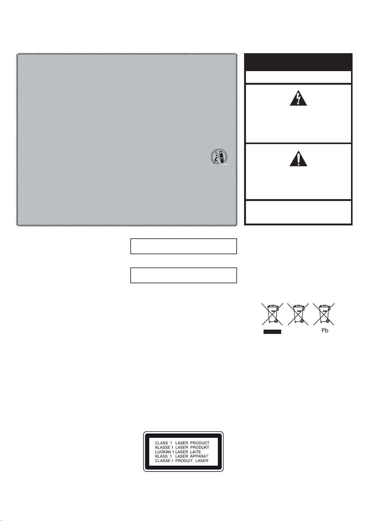
For CD/DVD/Blu-ray Disc™Players:
Caution:
This product uses a laser system. To prevent direct exposure
to the laser beam, do not open the cabinet enclosure or defeat
any of the safety mechanisms provided for your protection.
DO NOT STARE INTO THE LASER BEAM.To ensure proper use
of this product, please read the owner’s manual carefully and
retain it for future use. Should the unit require maintenance
or repair, please contact your local Harman Kardon service
center. Refer servicing to qualified personnel only.
For Products That Include Batteries:
Instructions for Users on Removal and Disposal of
Used Batteries.
CAUTION
Risk of explosion if battery is incorrectly replaced.
Replace only with the same or equivalent type.
Alkaline batteries are considered nonhazardous.
Rechargeable batteries (i.e., nickel cadmium, nickel metal-
hydride, lithium and lithium-ion) are considered hazardous
household materials and may pose an unnecessary health
and safety risk.
In the European Union and other locations, it is illegal to
dispose of any battery with household trash. All batteries
must be disposed of in an environmentally sound manner.
Contact your local waste management officials for information
regarding the environmentally sound collection, recycling and
disposal of used batteries.
To remove the batteries from your equipment or remote
control, reverse the procedure described for inserting
batteries in the owner’s manual.
For products with a built-in battery that lasts for the lifetime of
the product, removal may not be possible for the user. In this
case, recycling or recovery centers handle the dismantling of
the product and the removal of the battery. If, for any reason, it
becomes necessary to replace such a battery, this procedure
must be performed by authorized service centers.
Important Safety Instructions
CAUTION
RISK OF ELECTRIC SHOCK. DO NOT OPEN.
THE LIGHTNING FLASH WITH AN ARROWHEAD SYMBOL,
WITHIN AN EQUILATERAL TRIANGLE, IS INTENDED TO
ALERT THE USER TO THE PRESENCE OF UNINSULATED
“DANGEROUS VOLTAGE” WITHIN THE PRODUCT’S
ENCLOSURE THAT MAY BE OF SUFFICIENT MAGNITUDE TO
CONSTITUTE A RISK OF ELECTRIC SHOCK TO PERSONS.
THE EXCLAMATION POINT WITHIN AN EQUILATERAL
TRIANGLE IS INTENDED TO ALERT THE USER TO
THE PRESENCE OF IMPORTANT OPERATING AND
MAINTENANCE (SERVICING) INSTRUCTIONS IN THE
LITERATURE ACCOMPANYING THE PRODUCT.
WARNING: TO REDUCE THE RISK OF FIRE OR ELECTRIC
SHOCK, DO NOT EXPOSE THIS APPARATUS TO RAIN OR
MOISTURE.
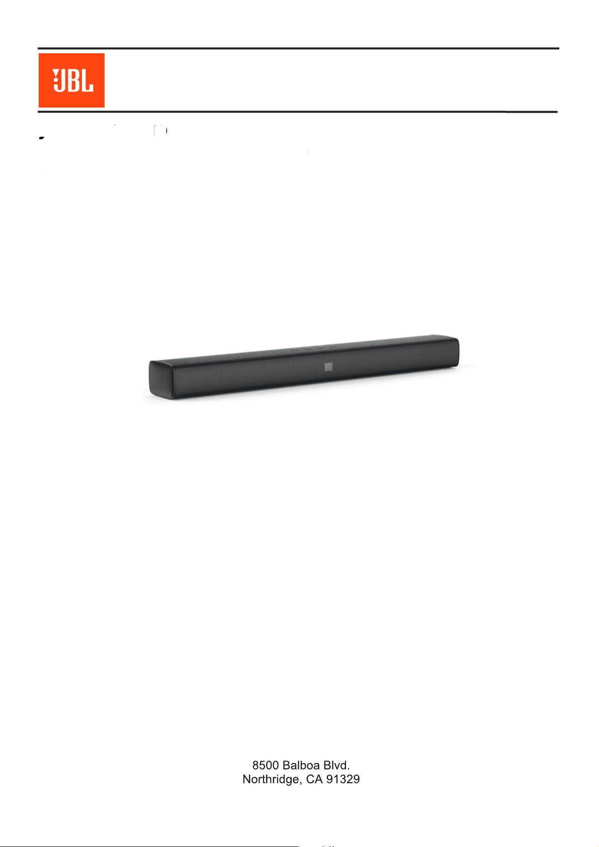
BDS 270 / BDS 570 harman/kardon
2 of 86
3-1

Each precaution in this manual should be followed during servicing.
Components identified with the IEC symbol in the parts list are special significance to safety. When replacing a component identified with
, use only the replacement parts designated, or parts with the same ratings or resistance, wattage, or voltage that are designated in the
parts list in this manual. Leakage-current or resistance measurements must be made to determine that exposed parts are acceptably
insulated from the supply circuit before retuming the product to the customer.
Some semiconductor (solid state) devices can be damaged easily by static electricity. Such components commonly are called
Electrostatically Sensitive (ES) Devices. Examples of typical ES devices are integrated circuits and some field effect transistors and
semiconductor "chip" components.
The following techniques should be used to help reduce the incidence of component damage caused by static electricity.
1. Immediately before handling any semiconductor component or semiconductor-equipped assembly, drain off any electrostatic charge on
your body by touching a known earth ground. Alternatively, obtain and wear a commercially available discharging wrist strap device,
which should be removed for potential shock reasons prior to applying power to the unit under test.
2. After removing an electrical assembly equipped with ES devices, place the assembly on a conductive surface such as aluminum foil, to
prevent electrostatic charge build-up or exposure of the assembly.
3. Use only a grounded-tip soldering iron to solder or unsolder ES devices.
4. Use only an anti-static solder removal device. Some solder removal devices not classified as "anti-static" can generate electrical charges
sufficient to damage ES devices.
5. Do not use freon-propelled chemicals. These can generate electrical change sufficient to damage ES devices.
6. Do not remove a replacement ES device from its protective package until immediately before you are ready to install it. (Most replacement
ES devices are packaged with leads electrically shorted together by conductive foam, aluminum foil or comparable conductive material.)
7. Immediately before removing the protective material from the leads of a replacement ES device, touch the protective material to the
chassis or circuit assembly into which the device will be installed.
Be sure no power is applied to the chassis or circuit, and observe all other safety precautions.
8. Minimize bodily motions when handling unpackaged replacement ES devices. (Otherwise harmless motion such as the brushing together
or your clothes fabric or the lifting of your foot from a carpeted floor can generate static electricity sufficient to damage an ES devices.
CAUTION :
-2

SAFETY PRECAUTIONS
The following check should be performed for the continued
protection of the customer and service technician.
LEAKAGE CURRENT CHECK
Measure leakage current to a known earth ground (water
pipe, conduit, etc.) by connecting a leakage current tester
between the earth ground and all exposed metal parts of the
appliance (input/output terminals, screwheads, metal
overlays, control shaft, etc.). Plug the AC line cord of the
appliance directly into a 120V AC 60Hz outlet and turn the
AC power switch on. Any current measured must not exceed
o.5mA.
ANY MEASUREMENTS NOT WITHIN THE LIMITS
OUTLINED ABOVE ARE INDICATIVE OF A
POTENTIAL SHOCK HAZARD AND MUST BE
CORRECTED BEFORE RETURNING THE APPLIANCE
TO THE CUSTOMER.
Device
under
test
Test all
exposed metal
surfaces
Also test with
plug reversed
(Using AC adapter
plug as required)
AC Leakage Test
Leakage
current
tester
Reading should
not be above
0.5mA
Earth
ground
3-3

Software Upgrade Method
1.Copy MCU software **.BIN to USB driver root catalog, and rename **.BIN to “JBLBAR.BIN”.
2. Power on the Unit set, change to USB source.
3. Insert USB to Unit set, the Unit set will read the software and grape LED fast flash.
4. Press and hold “power & volume - ” till the grape LED start to slow flash, then start upgrading
5. The upgrade stage will continue 14 - 16 minutes, after finished upgrade, 5 LEDs light
white light 2s, then Unit set will restart.
Software version information check method:
1. Unit set power on and change to BT source, press and hold RC night mode key 5s,
then it will read out present software version, such as “two, one”.
SOFTWARE UPGRADE METHOD AND CHECK INSTRUCTION

Dismantling Instructions

Dismantling Instructions

Dismantling Instructions

Dismantling Instructions - Remove PCBA

Dismantling Instructions

Reassembly Procedure
Solder the full range
speaker and the tweeter
and capacitor before other
reassembly process.
Note: one pin of the
capacitor is welded to the
positive pole of the full
range speaker, another pin
is welded with the negative
pole of the tweeter.

2
HARMAN INTERNATIONAL. CONFIDENTIAL. COPYRIGHT 2013.
Block Diagram
5V
ME6211
ME6213
18V AMP
18V/2A
AP4435
SW
SY8213 3V3_MCU
5V
R
Channel
L Channel
15W 4 Ω
Aux in
SW upgrading/ USB
Playing
BT
ATS2825
buttons DSP
MTK8307
Amp
TAS5709
I2S
BT ANT
Flash
15W 4Ω
Uart
LDO 1.25V
I2C
LEDs
Flash
USB
Spdi
f
Optical
DC cable 2.2m
RC IR
3V3_BT
DSP
CS4810
I2S
HDMI Output

SET WIRING DIAGRAM
LED board IRboard
Mainboard
Buttonboard Speaker

Power Line
Control Line
Audiol Line
MT8307OQE
AUX INPUT
OPT INPUT
ARC
TAS5731M
AMP
Power KEY
Source KEY
Vol+/- KEY
Purple/Whitex1
Blue/Whitex1
Green/Whitex1
Amber/Whitex1
FLASH
MX25L3206EM2
SPI
POWER
Adapter
19V2A
DC TODC
MP9942
5V
I2S
I2C
LDO3.3V
LP3986
DSP
IR
LDO1.2V
M1.2V
M3.3V
TOMCU
TOMCU
M1.2V M3.3V
B3.3V
19V
TOAmp
19V
EN
4OHM15W
4OHM15W
HDMI OUT
MOS
DSP
CS48L10 I2S
USB JACK
USB IN
BT MODULE
ATS2825C
SPDIF
UART TX RX
EN DFU
FLASH 32M
RST PDN
ESMT SDRAM
M12L64164A
+ 5V
BT4V
I2C
I2C
SPI
4435
B3.3V
C1.2V
LDO3.3V B3.3V TODSP 48L10
LDO1.2V
C1.2V TODSP 48L10
EN
+ 5V
MOS
3407
LP3986
LDO4V
LP3983
BT4V
TOBT
AMP
Amber/Whitex1
BOOMTECH
SPI
RST PDN
AS1117
TOSDRAM
LP3986
LDO3.3V S3.3V
S3.3V
LPW5210
I2C
AW9523
27MHZ 74LVC2G04
12.288MHZ
BT RF
26MHZ
BLOCK DIAGRAM

SHEET: 2/5
AMP
FromNo :FM QMP005 13
B
C
D
B
C
D
V1
V5
V4
V3
V2
A
1
ISS 5
A
4
TITLE:Schematic Diagram
32
54321
APPROVAL CHECKED DESIGN
WangYC TangB
SCALE: FREE
REV: V1
CHANGE RECORDS DATE REVISER
PROTOTYPE-A3
CONFIDENTIAL UNDER NDA
MODEL:BT-0520
20170707 ZXB ZXB
Part NO:NA
1.25*(1+10/1000) = 1.25V
L_CH
R_CH
4OHM
15W
15W
4OHM
8307 POWER PART 1.25V/3.3V
5V POWER SWPART(TODSP AMP)
AMP POWER SWPART
DC TODC PART (19V TO5V)
AMP PART
DC IN PART
DSP AMP 3.3V POWER
2C41
0.1u16V
2C42
22u6.3V
2C43
0.1u16V
2C44
22u6.3V
L9
FB600
2C45
0.1u16V
2C46
22u6.3V
2C47
0.1u16V
2C48
22u6.3V
L11
FB600
R29
1K
R30
10R
1GND
2
OUT
3VIN
U1
AS1117-1.2V
L5 10uH2A
C242
22UF/25V
R139 15K
R141
100K
R78
20R
R136
82K
C243
0.1u/50
C246
0.1uF16V
C247
0.1u/50
C248
0.1UF
1
2
C250
100u10V
C221
10uF10V
L7
FB600
R21
100K
R22 100K
1S
2S
3S
4G
5
D6
D7
D8
D
Q12
AP4435GM
1
23
Q1
3904
C25
0.1u50V
R23 10K
R24
18K
C26
0.1u50V
R51
100K
R63 100K
C31
2.2u10V
1
23
Q2
3904
C32
10nF
R64 10K
R65
18K
G
SD
Q10
GV3407
1PG
2IN
3SW
4GND 5
BST
6
EN
7
VCC
8
FB
U17
IC-MP9942
R111 1M
R112 200K
C52
47P
R113
51K
1OUT_A
2PVDD_AB
3PVDD_AB
4BST_A
5NC
6SSTIMER
7NC
8PBTL
9AVSS
10 PLL_FLTM
11 PLL_FLTP
12 VR_ANA
13 AVDD
14 ADR/FAULT
15 MCLK
16 OSC_RES
17 DVSSO
18 VR_DIG
19 PDN
20 LRCK
21 SCLK
22 SDIN
23 SDA
24 SCL
25
RESET 26
STEST 27
DVDD 28
DVSS 29
GND 30
AGND 31
VRGE 32
GVDD_OUT 33
BST_D 34
PVDD_CD 35
PVDD_CD 36
OUT_D
37
PGND_CD 38
PGND_CD 39
OUT_C 40
NC 41
NC 42
BST_C 43
BST_B 44
NC 45
NC 46
OUT_B 47
PGND_AB 48
PGND_AB
2U2
TAS5731M
2R19
22R
2R20
22R
2R21
1K
2C50
102
2C51
0.1u16V
2C54
10u6.3V
2L5
FB600
2C55
0.1u25V
2C59
1u25V
2R23
18.2K
2C60 4.7u10V
2C62 0.1u16V
2C63 0.1u16V
2C76
10u6.3V
2L6
FB600
2C77 4700P50V
2C78
0.047u25V
2C79
4700P50V
2R24
470R
2C80
2200P50V
2C81
0.68u50v
2C82
0.68u50v
2C83
0.01u50V
2C84
0.01u50V
2C85
0.68u50v
2C86
0.68u50v
2C87
0.01u50V
2C88
0.01u50V
2R25
15K
2R26 4R7
2C89
0.1u25V
2C90
0.1u25V
2C91
10u25V
2C92
10u25V
2C93
47P
2C94
47P
2C95 47P
2C96 47P
2R27
20R
2C97
330P
2R28
20R
2C98
330P
2R29
20R
2C99
330P
2R30
20R
2C100
330P
2C101
0.047u25V 2R31
470R
2R42
10K
RT2 100R
1
2
2C107
470u25V
1
2
2C108
3300u25V
L15 22uH/3A
L21
22uH/3A
L4 22uH/3A
L23
22uH/3A
1
2
2C103
470u25V
TP51
TP52
TP53
TP54
C19
22UF/25V
1
2
2J1
1
2
2J2
L24 NC
1
2
C44
100uF25V
C7
0.1u/50
1
2
3
J3
19V 2A
C8
0.1u/50
TP6
TP7
L2
NC
2C56
0.1u16V
2C57
22u6.3V
2C58
0.1u16V
2C61
22u6.3V
L22
FB600
2C72
0.1u16V
2C73
22u6.3V
2C74
0.1u16V
2C75
22u6.3V
L13
FB600
2C1
22P
2C2
0.1u16V
2C3
22u6.3V
2C4
0.1u16V
2C5
22u6.3V
L19
FB600
L16
120R/100M
L17
120R/100M
1
VOUT
2GND
3VIN
U3 LP3986-33B3F
1
VOUT
2GND
3VIN
U14 LP3986-1V2
1
VOUT
2GND
3VIN
U4 LP3986-33B3F
1
VOUT
2GND
3VIN
U18
LP3986-33B3F
L18
FB600
L20
FB600
L26
FB600
L28
FB600
C128
102
C129
102
C133
102
C134
102
C142
102
C143
102
2C20
102P
2C21
102P
2C22
102P
2C23
102P
L29
NC
L30
NC
L45
NC
L46
NC
1
2
3
4
L3
C154
0.1u/50 C155
0.1u/50
C156
0.1u/50
C158
0.1u/50
C159
22UF/25V
C160
22UF/25V
L31
FB60
C38
102
DC5V
MCU3.3V
DC5V
MCU1.25V
DC19V-IN DC5V
STB_5V
AMP_VCC19V
DC19V-IN
POWER_EN
SW+5V
DC5V
SW+5V-EN
48L10/5731/I2S/DATA
48L10/5731/LRCLK
48L10/5731/BCLK
BT/48L10/5731/SDA
BT/48L10/5731/SCL
AMP_PDN_AMP
AMP3.3V
AMP3.3V
AMP_VCC19V
AMP_VCC19V
AMP_RESET_AMP
DC19V-IN
SW+5V CS48L10/1.2V
SW+5V 48L103.3V
SW+5V AMP3.3V
830748L10/5731/MCLK

MCU SHEET: 3/5
FromNo.:FM-QMP005-13
B
C
D
B
C
D
V1
V5
V4
V3
V2
A
1
ISS 5
A
4
TITLE:Schematic Diagram
32
54321
APPROVAL CHECKED DESIGN
WangYC TangB
SCALE: FREE
REV: V1
CHANGE RECORDS DATE REVISER
PROTOTYPE-A3
CONFIDENTIAL UNDER NDA
MODEL:BT-0520
20170707 ZXB ZXB
Part NO:NA
MT8307OQE
MCU
USB IN PART
MCU PART
SPDIF IN PART
DEBUGPART
1AVDD12_2
2AVDD33_1
3XTALI
4XTALO
5V14
6GPO5
7AVDD33_2
8NC
9NC
10 GPIO2
11 USB_DP
12 USB_DM
13 VDD33_USB
14 PAD_VRT
15 VDD12_USB
16 DV_Y2
17 DV_Y3
18 DV_Y4
19 SF_CS_
20 SF_DO
21 SF_DI
22 DVDD33
23 SF_CK
24 UP1_6
25 UP1_7
26 GPIO11
27 GPIO6
28 PRST_
29 IR
30 GPIO3
31 GPIO4
32 DV_C0
33 DV_C1
34 DV_C2
35 DV_C3
36 SD_MS_D2
37 SD_MS_D3
38 GPIO13
39 GPIO9
40 GPIO8
41 GPIO7
42 DVDD33
43 RD0
44 RD1
45 RD2
46 RD3
47 RD4
48 RD5
49 RD6
50 RD7
51 DQM0
52 RD15
53 RD14
54 DVDD12
55 RD13
56 RD12
57 RD11
58 RD10
59 RD9
60 RD8
61 DQM1
62 RCLK
63 RA11
64 RA9
65
RA8 66
RA7 67
DVDD33 68
RA6 69
RA5 70
RA4 71
RWE_ 72
CAS_ 73
RAS_ 74
DVDD33 75
BA0 76
BA1 77
RA10 78
RA0 79
RA1 80
RA2 81
RA3 82
DVDD12 83
SPDIF 84
GPIO10 85
EXT_RES 86
AVDD33_12 87
TXCN 88
TXCP 89
AVDD12_C 90
TX0N 91
TX0P 92
AVSS12 93
TX1N 94
TX1P 95
AVDD12_D 96
TX2N
98
GPIO29 97
TX2P
99
GPIO30 100
GPIO31 101
GPIO32 102
GPI33 103
AVDD33 104
VREF/GPIO14 105
FS 106
IOC 107
AVDD33 108
AGND12 109
NC 110
NC 111
AKIN2/GPIO19 112
ADVCM/GPIO20 113
AKIN1/GPIO21 114
AADVDD 115
APLLVDD_GPIO/GPIO34 116
APLLCAP/GPIO35 117
ADACVSS 118
LFE/GPIO 119
ABCK 120
AR/GPIO0 121
AVCM 122
AL/GPIO 123
ALRCK 124
ASDATA0 125
ADACVDD1 126
ADACVDD2 127
AVDD12 128
NC
129
U5
MT8307_1
R55 100R
R56 470K
R68 0R
R69 0R
C56 0.1u16V
C57 0.1u16V
C58
2.2u6.3V
C59
0.1u16V
C60
0.1u16V
TP62
TP63
TP64
C61 0.1u16V
C62 1u6.3V
R71 5.1K_1%
R72 560R
R76 1K
R81 2.5K_1%
R820R
C63
0.1u16V
C64
4.7u16V
C65
0.1UF/16V
C66 10u10V
R83
0R
R84
10R
C67
0.1u16V
C68
0.1u16V
C79
0.1u50V
C80
1u10V
C82
0.1u16V
R85
0R
R86 0R
R87 4R7
C87 10u6.3V
C88 1u10V
C89 0.1u16V
C90
0.1u16V
C91
0.1u16V
C92
0.1u16V
C93
0.1u16V
C94
0.1u16V
C95 10UF
C96 10PF
R99 15K_1%
R100
4.7K_1%
R101
10K
R102 22K
R104
3.9K
1
2
3
Q4
2N3904
1
2
3
Q5
2N3904
C99 1u6.3V
R107
4.7K
R108
4.7K
C100 0.1u16V
R143 100R
C179
0.1u16V
1
2
C102
22uF/6.3V
1
2
C169
220UF/10V
Y2 27M
C103 10P
C104
10P
C105
0.1u16V
C118
10u6.3V
R25
100R R26
100R R27
100R
R31
22R
R7 0R
R15 0R
D23
NC D24
NC
C97
10uF
C98
0.1u16V
R89 4R7
C86 0.1u16V
1
2
C101 100uF/10V
C108 22P
C109 47P
C113 47P
C30 47P
1
S
2
G
3D
Q3
WNM2306
R110 47R
C51
22PF
C71
1u10V
L10 FB600
R6
47K
C5
22u6.3V
C6
0.1u16V
1C21
22P
TP9
TP10
FB6
FB600
FB5
FB600
D1 ESD
D2 ESD
D10 ESD
1VBUS
2D-
3D+
4VSS
5
SHLD
6
SHLD
J6
C9 22P
C10 22P
C110.1u16V
C12
22u6.3V
TP24
TP25
TP26
TP27
R36
10R
R52
10R
L12 NC
TP57
1VOUT
2GND
3VCC
45
J2 OPTICAL
R132 51R
R133 0R
1
2
3
4
5
6
7
89
10
11
12
13
14
15
16
R137
22R
1
2
3
4
5
6
7
89
10
11
12
13
14
15
16
R149 22R
R150 22R
R151 22R
R152 22R
1
2
3
4
5
6
7
89
10
11
12
13
14
15
16
R134 22R
1
2
3
4
5
6
7
89
10
11
12
13
14
15
16
R135 22R
C390.001u16V
C400.001u16V
C41 0.001u16V
1
2
3
4
5
6
7
89
10
11
12
13
14
15
16
R155
100R
1
2
3
Q7
2N3904
R157
4.7K
1C1 103
R160
100K
R161 4.7K
R162
22R
12
FB3
FB600
C112 NC
C115
102
C116
102
C117
102
C119
102
C1200.001u16V
C1240.001u16V
12
FB8 FB600
12
FB10 FB600
12
FB11 FB600
12
FB12 FB600
12
FB13 FB600
1
2
3
4
5
6
7
89
10
11
12
13
14
15
16
R1
100R
R16
100R
C37
104
1
2
3
45
6
7
8RT3
10R
12
FB14 FB600
12
FB17
FB600
C152
22PF
C153
22PF
C161
0.001u16V
C162
0.001u16V
C163 22PF
C170
0.01uF/50V
R41 100R
R42 100R
R46 100R
C15 22PF
C16 22PF
C17 22PF
C180 0.1UF
C181 10PF
C182 10PF
C185 22PF
C186 0.1UF
1C2
NC
R12 1K
R35 1K
C187 100PF
C188 100PF
C190
104 C191
100PF C192
100PF
C193 NC
C194 NC
C195 NC
R74 100R
C197 100P
TP70
3.3V
TP71
RX
TP72
TX
TP73
GND
R103
1K
R114
1K C205
1u6.3V
C206
1u6.3V
R144
2.2M
R164
2.2M
R168
12K
R170
12K
C207
2.2u6.3V
R17410K
R175 10K
R176
1M
C208
0.015u
1
2
3
Q8
2SC2712
1
2
3
Q9
2SC2712
1
2
3
Q11
2SC2712
13
2
Q13
BAT54C
C172 0.1UF
D27
TVS LESD8L3.3CT5G
C183 47PF
D33
403906640109
C220 NC
C222 100PF
ARC-SPDIF-8307
DP
DM
MA3
MA2
MA1
MA0
MA10
BA1
BA0
RAS#
CAS#
WE#
MA4
MA5
MA6
MA7
MA8
MA9
MA11
DCLK
DQM1
DQ8
DQ9
DQ10
DQ11
DQ12
DQ13
DQ14
DQ15
DQM0
DQ6
DQ5
DQ4
DQ3
DQ2
DQ1
DQ0
BT-UART-RX
BT-UART-TX
CEC
RS232RX
HDIMI/8307/SCL
HDIMI/8307/SDA
TX2-
TX1+
TX1-
TX0+
TX0-
TXC+
TXC-
SF_CS
SF_DO
SF_DI
SF_CK
RS232RX
RS232TX
RS232TX
MCU3.3V
8307/CS48L10/I2S/DATA
8307/48L10/I2S_LRCK
8307/48L10/I2S_BCK
TX2+
HPLG
SDRAM3.3V-2
STB_5V
MCU3.3V
MCU1.25V
MCU3.3V
MCU1.25V
MCU3.3V
MCU3.3V
MCU3.3V
MCU1.25V
MCU3.3V
MCU3.3V
MCU1.25V
OPT-SPDIF-IN
BT-SPDIF-IN
MCU3.3V
V1P4
RFV12_1
KEY-VOL-
IR
KEY-POWER
KEY-VOL+
KEY-SOURER
SDRAM3.3V-2
OPT-SPDIF-IN
USB+5V
DM
DP
2825INT
830748L10/5731/MCLK
DQ7
BT2825INT2
OPTDET
OPTDET
AUXDET
AUXDET
SDRAM3.3V-2
AUXDETR
AUXDETL

SHEET: 4/5
SDRAM+DSP
B
C
D
B
C
D
V1
V5
V4
V3
V2
A
1
ISS 5
A
4
TITLE:Schematic Diagram
32
54321
APPROVAL CHECKED DESIGN
WangYC TangB
SCALE: FREE
REV: V1
CHANGE RECORDS DATE REVISER
PROTOTYPE-A3
MODEL:BT-0520
20170707 ZXB ZXB
Part NO:NA
8307 SDRAMPART
MHL/HDMI
TX
DSP PART
8307 FLASH PART
HDMI ARC PART
AUX IN PART
1
VCC
2
DQ0
3
VCCQ
4
DQ1 5
DQ2
6
VSSQ
7
DQ3 8
DQ4
9
VCCQ
10
DQ5 11
DQ6
12
VSSQ
13
DQ7
14
VCC
15 DQML
16 WE
17 CAS
18 RAS
19 CS
20 BA0/A13
21 BA1/A12
22 A10/AP
23 A0
24 A1
25 A2
26 A3
27
VCC
28 VSS
29 A4
30 A5
31 A6
32 A7
33 A8
34 A9
35 A11
36 NC
37 CKE
38 CLK
39 DQMH
40 NC
41 VSS
42
DQ8
43
VCCQ
44
DQ9 45
DQ10
46
VSSQ
47
DQ11 48
DQ12
49
VCCQ
50
DQ13 51
DQ14
52
VSSQ
53
DQ15
54 VSS
U10
ESMTM12L64164A
R14210K
R145 10K
C121
NC
R148 0R
C122 0.1u16V
C123 0.1u16V
C125 0.1u16V
C1260.1u16V
C127 0.1u16V
C135 0.1u16V
C136 0.1u16V
C137 0.1u16V
3
RX2-/NC
1
RX2+/NC 2
SHLD2/CDS
4
RX1+/NC
6
RX1-/NC
15
SCL/CDP 16
SDA/NC
7
RX0+/MHL+
9
RX0-/MHL-
5
SHLD1/GND
11
SHLDC/GND
14
HEAC+/NC
18
+5V/VBUS
13
CEC/NC
19
HPD/HEAC-
10
RXC+/NC
12
RXC-/NC
8
SHLD0/GND
17
GND
20
GND 21
GND 22
GND 23
GND
J16
HDMI_A
R165
0R
R166
0R
C138
0.1u16V
C139
22UF/6.3V
C140
22uF/6.3V
FB4
600@100M D8
SBRT5A50SA
C149
1u
R169
20R
C141
47P
R172
27K
R173
NC
D9
1N4148
R178 1.8K
R179 1.8K
FB20
600@100M
R180
10K
FB9
600@100M
1
CLK 2
VPLL 3
GND 4
VD 5
VL 6
CLK/SCL
7CS
8MISO/SDA
9MOSI
10 BUSY/HSO/EE_CS
11 INT/HS1
12 RESET
13 DBCK
14 VL1
15 GND1
16 VD1
17 DBDA
18 MCLK
19
DAO_D1 20
DAO_LRCLK 21
DAO_SCLK 22
DAI/_D1 23
DAI_LRCLK 24
DAI_SCLK
U9
CS48L10
L8
FB600
R120
33R R125
100R R127
100R
2C640.1u16V
2C65
22uF/6.3V
2C66 0.1u16V
2C67 0.1u16V
2C68
0.1u16V
2C69
22uF/6.3V
2C70
0.1u16V
2C71
0.1u16V
R116 4.7K
R121100R
C106
104
R122 4.7K
R123 4.7K
R119
100R
C114
NC
L1
FB600
R18
33R
1OUT
2GND
3OC 4
EN
5
IN
U7
LPW5210
R59
5.1K 1/CS
2SO
3/WP
4VSS 5
SI 6
SCK 7
/HOLD 8
VCC
U11
MX25L3206EM2I-12G)
R156 10K
R158 10K
R16310K
C146
0.1u16V
C130
22u6.3V
L14
FB600
2I2
3GND
5I4
10
O1
4I3
1I1
6
O4 7
O3
9
O2
U16
Rclamp0524
2I2
3GND
5I4
10
O1
4I3
1I1
6
O4 7
O3
9
O2
U12
Rclamp0524
2I2
3GND
5I4
10
O1
4I3
1I1
6
O4
7
O3
9
O2
U15
Rclamp0524
2
1A
3GND 5
VCC
41Y
U6
74LVC1G04GW
C22
0.1u16V
C23
22P
C24
1u10V
FB16
600@100M
R9
0R
C18
1u10V
R10 75
R11 10K
R8 10K
C3
33P
C4
33P
R2 8.2K
R3 8.2K
R4
9.1K
R5
9.1K
C13
2.2u16V
C14
2.2u16V
C1100P
C2 100P
TP2
TP3
TP5
D3 ESD
D6 ESD
R38
4.7K
R54
4.7K
R222 4.7K
R37 4.7K
R223 4.7K
R224 4.7K
R226
100R R227
100R
R228
100R
C147
33P C148
33P C150
33P C157
33P
R47
22R R48
22R R50
22R R53
22R R57
22R R61
22R
1
2
3
4
5
JK3
PJ-306
2C6
10PF
2C7
10PF
R117 1M
R126
1K
2C8
104
2C9
22UF/6.3V
FB2
600@100M
Y1
12.288M
11A
2GND
32A 4
2Y
5
VCC
6
1Y
U19
74LVC2G04
C110 0.1u16V
C111 22UF/6.3V
2C10
0.1u16V
2C11
22u6.3V
2C12
0.1u16V
2C13
22u6.3V
L25
FB600 1
VOUT
2GND
3VIN
U20
LP3986-33B3F
12
FB15 FB600
2C14
NC
2C15
NC
2C16
NC
2C17
NC
R40 47K
C171 100P
C173
10P
C174
10P
C175
100P
C176
100P
C177
0.1u
C189
0.1UF
C145 22UF/6.3V
L47
FB600/100M
L48 NC
L49 FB600/100M
L50 FB600/100M
L51 FB600/100M
R32 0R
C184
22P
C217
22u6.3V
C218
22u6.3V
C219
22u6.3V
MA0
MA1
MA2
MA3
MA4
MA5
MA6
MA7
MA8
MA9
MA10
MA11
BA0
BA1
RAS#
CAS#
WE#
DQM0
DQM1
DQ15
DQ14
DQ13
DQ12
DQ11
DQ10
DQ9
DQ8
DQ7
DQ6
DQ5
DQ4
DQ3
DQ2
DQ1
DQ0
DCLK
SDRMCU3.3V SDRAM3.3V-2
TX1+
TXC-
TXC+
TX0-
TX0+
TX2-
TX1-
TX2+
CEC
USB+5V
HDIMI/8307/SCL
HDIMI/8307/SDA
HPLG
ARC-SPDIF-IN
DC5V
CS48L10/1.2V
DSP_RESET
8307/CS48L10/I2S/DATA
8307/48L10/I2S_LRCK
8307/48L10/I2S_BCK
MISO
48L103.3V
8307/48L10/CLK
48L10/5731/I2S/DATA
USB+5V
SDRMCU3.3V
MCU3.3V
SF_CS
SF_DO SF_CK
SF_DI
ARC-SPDIF-8307
ARC-SPDIF-IN
48L103.3V
AUX_L
AUX_R
INT
BUSY
MOSI
CS
48L10/5731/BCLK
48L10/5731/LRCLK
830748L10/5731/MCLK
CLK
8307/48L10/CLK
3.3V
3.3V
DC5V SDRAM3.3V-2
AUXDETL
AUXDETR
SDRAM3.3V-2

SHEET: 5/5
BT
FromNo.:FM-QMP005-13
B
C
D
B
C
D
V1
V5
V4
V3
V2
A
1
ISS 5
A
4
TITLE:Schematic Diagram
32
54321
APPROVAL CHECKED DESIGN
WangYC TangB
SCALE: FREE
REV: V1
CHANGE RECORDS DATE REVISER
PROTOTYPE-A3
CONFIDENTIAL UNDER NDA
MODEL:BT-0520
20170707 ZXB ZXB
Part NO:NA
IR
GND
3.3V
IR PCB
KEY PCB
BT PART
IR CON PART
KEY CON PART
RST
GND
+3.3V
SDA
SCL
GND
LED AMBER
RST
GND
+3.3V
SDA
SCL
GND
LED AMBER
R19
2.7NH 1
23
RF1
RF
R14
1M/1.5M
C28 105
5VCC
2AGND
3DM
1VRO_S
4DP
6GPIOA17
7GPIOA20
8GPIOB7
9GPIOB8
10 GPIOB9
11 GND
12 GPIOA5
13 GPIOA21
14 GPIOA6
15 GPIOA23
16 GPIOA22
17 GPIOA15
18 GPIOA14
19 GPIOA13
20 GPIOA12
21 GPIOA11
22 GPIOA10
23 GPIOA9
24 GPIOA8
25 GPIOA16
26 SPI_MOSI
27 SPI_CLK
28 SPI_SS
29 GPIOB11
30 GND
31 BT_ANT 32
RTCVDD 33
NFC_WK_RTCVDD 34
GPIOA0 35
GPIOA1 36
GPIOA2 37
ONOFF 38
GND 39
BAT 40
DC5V 41
GPIOB0 42
GPIOA7 43
AVCC 44
AUX1R 45
AUX1L 46
AUX0L 47
AUX0R 48
AGND 49
SVCC 50
MICINR 51
MICINL 52
VRO 53
AOUTL 54
AOUTR
U2
ATS2825C
C29
LESD8L3.3CT5G
R17 10R
C69 104
C70
104
R201 100K
C75 1UF
C76 104
C77
0.5PF
C78 105
FB1
10R/1K_100MHZ
C81 104
R34
560K
C83
0.5PF
C84 105
TP8
C85 104
C196
22uF/6.3V
3V3
RX TX
R159
NC
R20 10R
R43 1K
R45 1K
1
2
3
4
CON1
4P
1M1
MARK(SMT)33
1M2
MARK(SMT)33
1M3
MARK(SMT)33
1M4
MARK(SMT)33
1M5
MARK(SMT)33
1M6
MARK(SMT)33
1
OUT 2
GND 3
VCC
IR1
HM540R
R98
10R
C47
0.1u16V
C46
4.7UF6.3V
C45 47P
D17 White
D14 White
D15 PURPLE
D12 BLUE
D13 White
D18 YELLOW
D19 White
TP11
TP12
TP55
R44 100R
R49 100R
TP43
D4 White
D5 GREEN
1
2
3
CON5
C131
22uF/6.3V
C132
0.1u25V
D21
LESD5L5.0CT1G
D7
LESD8L3.3CT5G
D20
NC
C27
0.1u16V
R94
10R
R28
10K
1VIN
2GND
3EN 4
FB
5
VOUT
U8 LP3983
R96
220K
R97
56K
R124
100R
R129
100R
R67 4.7K
R73 4.7K
C48 100P
C49 100P
TP4 TP13TP14
R33
10K
TP28
TP29
TP32
1
2
3
CON2
TP42
TP46
TP47
TP48 TP49 TP50
1
P10 2
P11 3
P12 4
P13 5
P00 6
P01
7
P02 8
P03 9
GND 10
P04 11
P05 12
P06
13 P07
14 P14
15 P15
16 P16
17 P17
18 AD0
19 SCL
20 SDA
21 VCC
22 INTN
23 RSTN
24 AD1
U13
IC-AW9523B
FB7 FB600
TP59
TP60
TP61
TP65
TP66
R147
0R
R140 NC
R62 1K
R58 100R
R60 100R
C21 22P
C33 22P
C34 22P
C35 104
C20 104
C36 10uF
R138 0R
R146
NC
D11
AMBER
R70
10R
R77
10R
R90
10R
R91
10R
R92
10R
R93 10R
R105 10R
R106 10R
R115 10R
R229 10R
R230 10R
R231 10R
R232 10R
R233 10R
R234 10R
R265 10R
R266 100R
R267 100R
R268 10R
R269
4.7K R270
4.7K
1
2
3
4
5
6
7
8
9
CON8
CON_SMT_07
1
2
3
4
5
6
7
8
9
CON3
CON_SMT_07
L27 FB600
R271
4.7K
R79 10K
TP1
R80 10K
R88 10K
R95 10K
TP15
1
2
3
4
5
6
CON6
1
2
3
4
5
6
CON7
L6 FB600
S4
SOURER
S1
VOL+
S2
VOL-
S3
POWER
TP16
TP17
TP18
TP19
TP20
TP21
TP22
TP23
TP30
TP31
R130 10R
R131
10R
R154 10k
R16710K
C42 104P
C43 104P
C50 104P
C53 104P
C54 104P
C55 100P
C72 100P
C74 22P
C107
102P
D16
103
D22
103
D25
103
D26
103
C144
102
C151
102
12
FB18
0R
TP104 TP40 TP41 TP44 TP45 TP56
C164
10PF
C166 100PF
C167
100PF
C168 10PF
TP58TP67TP68TP69
C178 104
R75 10K
C198
22PF
C199 100PF
C200
102PF
L32 FB600
L33 FB600
L34 FB600
L35
FB600
C201 100P
C202 100P
C203 100P
L37 1K
L38 1K
L39 1K
L40 1K
L41 1K
L42
FB600
L43 FB600
L44 FB600
C204
102PF
R177
NC
C165
1000PF
1
23
Q6
NC
R13
NC
C73
NC
R66 NC
R118 NC
C209
NC
1
23
Q14
NC
R128
NC
C210
NC
R181
NC
C211
NC
D28
ESD D29
ESD D30
ESD D31
ESD
D32
ESD
C212 104P
C213 104P
C214 104P
C215 104P
C216 104P
R39 2K
TP33TP34 TP39 TP75
TP76TP77TP78TP79TP80TP81
D34
LESD8L3.3CT5G
D35
LESD8L3.3CT5G
BT-SPDIF-IN
AUX_L
AUX_R
DC5V
BT-UART-RX
BT-UART-TX
DC5V
AMP_PDN_AMP
AMP_RESET_AMP
BTVCC
BT/48L10/5731/SCL
BT/48L10/5731/SDA
BTVCC
POWER_EN
SW+5V-EN
DSP_RESET
IR
SDRAM3.3V-2
KEY-VOL-
KEY-POWER
KEY-VOL+
KEY-SOURER
MCU3.3V
MOSI
CLK
CS
BUSY
INT
MISO
MCU3.3V
2825INT
D
BT2825INT2
DC19V-IN
LEDVCC
LEDCON1
LED-
LED-
LEDCON
LEDVCC
LEDCON LEDCON1
D
D

LAYOUT DIAGRAM - TOP VIEW
This manual suits for next models
10
Table of contents
Other JBL Speakers System manuals

JBL
JBL 4301E Manual

JBL
JBL VTX Series User manual

JBL
JBL SYNTHESIS S1S-EX User manual

JBL
JBL CS2165C User manual

JBL
JBL SRX900 Series User manual

JBL
JBL Bar 3.1 User manual

JBL
JBL Simply Cinema ESC350 User manual

JBL
JBL ES Series User manual

JBL
JBL Authentics L 16 User manual

JBL
JBL VerTec VT4889 Instruction sheet

JBL
JBL P-20t User manual

JBL
JBL DSC 500 User manual

JBL
JBL Simply Cinema ESC550 User manual

JBL
JBL STADIUM UB4100 User manual

JBL
JBL Project EVEREST DD66000 User manual

JBL
JBL SOUNDPOINT SP5II User manual

JBL
JBL Simply Cinema ESC333 User manual

JBL
JBL EON515XT/230 User manual

JBL
JBL NORTHRIDGE N24AWII User manual

JBL
JBL DUET III Quick start guide