Jennic JN5142 User manual

Data Sheet: JN5142
IEEE802.15.4 Wireless Microcontroller
© NXP Laboratories UK 2012 JN-DS-JN5142 1v0 1
Overview
Features: Transceiver
2.4GHz IEEE802.15.4 compliant
128-bit AES security processor
MAC accelerator with packet
formatting, CRCs, address check,
auto-acks, timers
Integrated ultra low power sleep
oscillator –0.5µA
2.0V to 3.6V battery operation
Deep sleep current 0.12µA
(Wake-up from IO)
0.5µA sleep with timer (1.5uA with
RAM held)
<$0.50 external component cost
Rx current 16.5mA
Tx current 14.8mA
Receiver sensitivity -95dBm
Transmit power 2.5dBm
Features: Microcontroller
32-bit RISC CPU, 1 to 32MHz
clock speed
Low power operation
Variable instruction width for high
coding efficiency
Multi-stage instruction pipeline
128KB ROM and 32KB RAM for
bootloaded program code
RF4CE or JenNet-IP software in
ROM
Master/Slave I2C interface.
3xPWM and Application
timer/counter
UART
SPI port with 3 selects
Supply Voltage Monitor with 8
programmable thresholds
2- to 4-input 8-bit ADC,
comparator
Battery and temperature sensors
Watchdog timer and Power-on-
Reset (with brown-out) circuit
Up to 18 DIO
Industrial temp -40°C to +125°C
6x6mm 40-lead Punched QFN
Lead-free and RoHS compliant
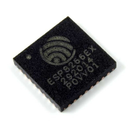
The JN5142 is an ultra low power, high performance wireless
microcontroller suitable for Remote Control, IEEE802.15.4 and Active RFID
applications. There is also a ROM variant that supports JenNet-IP Smart
Devices. The JN5142 features an enhanced 32-bit RISC processor offering
high coding efficiency through variable width instructions, a multi-stage
instruction pipeline and low power operation with programmable clock
speeds. It also includes a 2.4GHz IEEE802.15.4 compliant transceiver,
128KB of ROM, 32KB of RAM, and a comprehensive mix of analogue and
digital peripherals. The operating current is below 18mA, allowing operation
direct from a coin cell.
The peripherals support a wide range of applications. They include a 2-wire
serial interface, which operates as either master or slave, a two channel
ADC with battery and temperature sensors. A large switch matrix of up to 81
elements can be supported for remote control applications. The best in
class radio current and a 0.5µA sleep timer give excellent battery life.
Block Diagram
32-bit
RISC CPU Timer
UART
4-Chan 8-bit
ADC
Battery and,
Temp Sensors
2-Wire Serial
(Master)
SPI
128-bit AES
Encryption
Accelerator
2.4GH
z
Radio
2.4GHz
Radio
ROM
128KB
Power
Management
XTAL
O-QPSK
Modem
29-byte
OTP eFuse 2-Wire Serial
(Slave)
Sleep Counter
Watchdog
Timer
Watchdog
Timer
Voltage Supply
Monitor
RAM
32KB
IEEE802.15.4
MAC
Accelerator
Benefits
Single chip optimized for
simple applications
Very low current solution for
long battery life –over 10 yrs
RF4CE in ROM
Variant for JenNet-IP Smart
Devices
Highly featured 32-bit RISC
CPU for high performance
and low power
System BOM is low in
component count and cost
Flexible sensor interfacing
options
Applications
Robust and secure low power
wireless applications using
RF4CE
Remote Control
Toys and gaming peripherals
Active RFID tags
Point-to-point or star networks
using IEEE802.15.4
Energy harvesting, for example
self powered light switch
Smart Lighting Networks
Building Automation

2 JN-DS-JN5142 1v0 © NXP Laboratories UK 2012
Contents
1 Introduction 6
1.1 Wireless Transceiver 6
1.2 RISC CPU and Memory 6
1.3 Peripherals 7
1.4 Block Diagram 8
2 Pin Configurations 9
2.1 Pin Assignment 10
2.2 Pin Descriptions 12
2.2.1 Power Supplies 12
2.2.2 Reset 12
2.2.3 32MHz Oscillator 12
2.2.4 Radio 12
2.2.5 Analogue Peripherals 13
2.2.6 Digital Input/Output 13
3 CPU 15
4 Memory Organisation 16
4.1 ROM 16
4.2 RAM 17
4.3 OTP eFuse Memory 17
4.4 External Memory 17
4.4.1 External Memory Encryption 18
4.5 Peripherals 18
4.6 Unused Memory Addresses 18
5 System Clocks 19
5.1 16MHz System Clock 19
5.1.1 32MHz Oscillator 19
5.1.2 High-Speed RC Oscillator 20
5.2 32kHz System Clock 20
5.2.1 32kHz RC Oscillator 20
5.2.2 32kHz Crystal Oscillator 20
5.2.3 32kHz External Clock 21
6 Reset 22
6.1 Internal Brown-out Reset 22
6.2 External Reset 23
6.3 Software Reset 23
6.4 Supply Voltage Monitor (SVM) 23
6.5 Watchdog Timer 24
7 Interrupt System 25
7.1 System Calls 25
7.2 Processor Exceptions 25
7.2.1 Bus Error 25
7.2.2 Alignment 25
7.2.3 Illegal Instruction 25
7.2.4 Stack Overflow 25
7.3 Hardware Interrupts 26

© NXP Laboratories UK 2012 JN-DS-JN5142 1v0 3
8 Wireless Transceiver 27
8.1 Radio 27
8.1.1 Radio External Components 28
8.1.2 Antenna Diversity 28
8.2 Modem 30
8.3 Baseband Processor 31
8.3.1 Transmit 31
8.3.2 Reception 31
8.3.3 Auto Acknowledge 32
8.3.4 Beacon Generation 32
8.3.5 Security 32
8.4 Security Coprocessor 32
9 Digital Input/Output 33
10 Serial Peripheral Interface 35
11 Timers 38
11.1 Peripheral Timer/Counters 38
11.1.1 Pulse Width Modulation Mode 39
11.1.2 Capture Mode 39
11.1.3 Counter/Timer Mode 40
11.1.4 Delta-Sigma Mode 40
11.1.5 Example Timer/Counter Application 41
11.2 Tick Timer 41
11.3 Wakeup Timers 42
11.3.1 RC Oscillator Calibration 43
12 Pulse Counters 44
13 Serial Communications 45
13.1 Interrupts 46
13.2 UART Application 46
14 JTAG Debug Interface 48
15 Two-Wire Serial Interface (I2C) 49
15.1 Connecting Devices 49
15.2 Clock Stretching 50
15.3 Master Two-wire Serial Interface 50
15.4 Slave Two-wire Serial Interface 52
16 Random Number Generator 53
17 Analogue Peripherals 54
17.1 Analogue to Digital Converter 54
17.1.1 Operation 55
17.1.2 Supply Monitor 56
17.1.3 Temperature Sensor 56
17.2 Comparator 56
18 Power Management and Sleep Modes 57
18.1 Operating Modes 57
18.1.1 Power Domains 57

4 JN-DS-JN5142 1v0 © NXP Laboratories UK 2012
18.2 Active Processing Mode 57
18.2.1 CPU Doze 57
18.3 Sleep Mode 57
18.3.1 Wakeup Timer Event 58
18.3.2 DIO Event 58
18.3.3 Comparator Event 58
18.3.4 Pulse Counter 58
18.4 Deep Sleep Mode 58
19 Electrical Characteristics 59
19.1 Maximum Ratings 59
19.2 DC Electrical Characteristics 59
19.2.1 Operating Conditions 59
19.2.2 DC Current Consumption 60
19.2.3 I/O Characteristics 61
19.3 AC Characteristics 61
19.3.1 Reset and Supply Voltage Monitor 61
19.3.2 SPI Master Timing 63
19.3.3 Two-wire Serial Interface 64
19.3.4 Wakeup and Boot Load Timings 64
19.3.5 Bandgap Reference 65
19.3.6 Analogue to Digital Converters 65
19.3.7 Comparator 66
19.3.8 32kHz RC Oscillator 66
19.3.9 32kHz Crystal Oscillator 67
19.3.10 32MHz Crystal Oscillator 67
19.3.11 High-Speed RC Oscillator 68
19.3.12 Temperature Sensor 68
19.3.13 Radio Transceiver 69
Appendix A Mechanical and Ordering Information 75
A.1 SOT618-1 HVQFN40 40-pin QFN Package Drawing 75
A.2 Footprint information 76
A.3 Ordering Information 78
A.4 Device Package Marking 79
A.5 Tape and Reel Information 80
A.5.1 Tape Orientation and Dimensions 80
A.5.2 Reel Information: 180mm Reel 81
A.5.3 Reel Information: 330mm Reel 82
A.5.4 Dry Pack Requirement for Moisture Sensitive Material 82
Appendix B Development Support 83
B.1 Crystal Oscillators 83
B.1.1 Crystal Equivalent Circuit 83
B.1.2 Crystal Load Capacitance 83
B.1.3 Crystal ESR and Required Transconductance 84
B.2 32MHz Oscillator 85
B.3 32kHz Oscillator 87
B.4 JN5142 Module Reference Designs 89
B.4.1 Schematic Diagram 89
B.4.2 PCB Design and Reflow Profile 92
B.4.3 Moisture Sensitivity Level (MSL) 92

© NXP Laboratories UK 2012 JN-DS-JN5142 1v0 5
Related Documents 93
RoHS Compliance 93
Status Information 93
Disclaimers 94
Version Control 94
Contact Details 95

6 JN-DS-JN5142 1v0 © NXP Laboratories UK 2012
1 Introduction
The JN5142 is an IEEE802.15.4 wireless microcontroller that provides a fully integrated solution for applications
using the IEEE802.15.4 standard in the 2.4 - 2.5GHz ISM frequency band [1], including RF4CE. A ROM variant
provides support for JenNet-IP “Smart Device” applications such as lighting and building automation.
Applications that transfer data wirelessly tend to be more complex than wired ones. Wireless protocols make
stringent demands on frequencies, data formats, timing of data transfers, security and other issues. Application
development must consider the requirements of the wireless network in addition to the product functionality and user
interfaces. To minimise this complexity, NXP provides a series of software libraries and interfaces that control the
transceiver and peripherals of the JN5142. These libraries and interfaces remove the need for the developer to
understand wireless protocols and greatly simplifies the programming complexities of power modes, interrupts and
hardware functionality.
In view of the above, it is not necessary to provide the register details of the JN5142 in the datasheet.
The device includes a Wireless Transceiver, RISC CPU, on chip memory and an extensive range of peripherals.
1.1 Wireless Transceiver
The Wireless Transceiver comprises a 2.45GHz radio, a modem, a baseband controller and a security coprocessor.
In addition, the radio also provides an output to control transmit-receive switching of external devices such as power
amplifiers allowing applications that require increased transmit power to be realised very easily. Appendix B.4,
describes a complete reference design including Printed Circuit Board (PCB) design and Bill Of Materials (BOM).
The security coprocessor provides hardware-based 128-bit AES-CCM* modes as specified by the IEEE802.15.4
2006 standard. Specifically this includes encryption and authentication covered by the MIC –32/-64/-128, ENC and
ENC-MIC –32/-64/-128 modes of operation.
The transceiver elements (radio, modem and baseband) work together to provide IEEE802.15.4 (2006) MAC and
PHY functionality under the control of a protocol stack. Applications incorporating IEEE802.15.4 functionality can be
developed rapidly by combining user-developed application software with a protocol stack library.
1.2 RISC CPU and Memory
A 32-bit RISC CPU allows software to be run on-chip, its processing power being shared between the IEEE802.15.4
MAC protocol, other higher layer protocols and the user application. The JN5142 has a unified memory architecture,
code memory, data memory, peripheral devices and I/O ports are organised within the same linear address space.
The device contains 128kbytes of ROM, 32kbytes of RAM and a 29-byte One Time Programmable (OTP) eFuse
memory.

© NXP Laboratories UK 2012 JN-DS-JN5142 1v0 7
1.3 Peripherals
The following peripherals are available on chip:
Master SPI port with three select outputs
UART with support for hardware or software flow control
One programmable Timer/Counter which supports Pulse Width Modulation (PWM) and capture/compare, plus
three PWM timers which support PWM and Timer modes only.
Two programmable Sleep Timers and a Tick Timer
Two-wire serial interface (compatible with SMbus and I2C) supporting master and slave operation
Eighteen digital I/O lines (multiplexed with peripherals such as timers and UARTs)
8-bit, Analogue to Digital converter with up to four input channels
Programmable analogue comparator
Internal temperature sensor and battery monitor
Two low power pulse counters
Random number generator
Watchdog Timer and Supply Voltage Monitor
JTAG hardware debug port
User applications access the peripherals using the Integrated Peripherals API. This allows applications to use a
tested and easily understood view of the peripherals allowing rapid system development.

8 JN-DS-JN5142 1v0 © NXP Laboratories UK 2012
1.4 Block Diagram
Wireless
Transceiver
32-bit RISC CPU SPI
Master
MUX
UART0
Security Processor
Digital Baseband
Radio
Programmable
Interrupt
Controller
Timer0
2-wire
Interface
SPICLK
SPIMOSI
SPIMISO
SPISEL0
From Peripherals
RF_IN
VCOTUNE
Tick Timer
Voltage
Regulators 1.8V
VDD1
VDD2
IBAIS
VB_XX
SPISEL1
SPISEL2
TXD0
RXD0
RTS0
CTS0
TIM0CK_GT
TIM0CAP
TIM0OUT
SIF_D
SIF_CLK
Pulse
Counters PC0
PC1
JTAG
Debug
JTAG_TDI
JTAG_TMS
JTAG_TCK
JTAG_TDO
RAM
32KB ROM
128KB OTP
eFuse
Antenna
Diversity ADO
ADE
CPU and 16MHz
System Clock
32kHz Clock
Generator
XTAL_IN
XTAL_OUT
Clock
Divider/
Multiplier
High-speed
RC Osc
Watchdog
Timer
Voltage Supply
Monitor
Reset
Wakeup
Timer1
Wakeup Timer0
RESETN
32kHz Clock
Select 32KIN
Comparator1
COMP1P*
COMP1M*
ADC
M
U
X
ADC4*
ADC1
VREF/ADC2
ADC3*
Temperature
Sensor
Supply Monitor
32kHz
RC
Osc
32kHz
Clock
Gen
32KXTALIN
32KXTALOUT
PWMs
*Multiplexed with DIO pins
PWM1
PWM3
PWM2 DIO6/TXD0/JTAG_TDO/PWM2
DIO7/RXD0/JTAG_TDI/PWM3
DIO4/CTS0/JTAG_TCK/TIM0OUT
DIO5/RTS0/JTAG_TMS/PWM1/PC1
DIO17/COMP1M/SIF_D
DIO10/TIM0OUT/32KXTALOUT
DIO0/SPISEL1/ADC3
DIO3/RFTX/TIM0CAP
DIO2/RFRX/TIM0CK_GT
DIO1/SPISEL2/PC0/ADC4
DIO9/TIM0CAP/32KXTALIN
DIO8/TIM0CK_GT/PC1
DIO13/PWM3/ADE/RTS0/JTAG_TMS
DIO11/PWM1
DIO12/PWM2/ADO/CTS0/JTAG_TCK
DIO14/SIF_CLK/TXD0/JTAG_TD0/SPISEL1
DIO15/SIF_D/RXD0/JTAG_TDI/SPISEL2
DIO16/COMP1P/SIF_CLK
Figure 1: JN5142 Block Diagram

© NXP Laboratories UK 2012 JN-DS-JN5142 1v0 9
2 Pin Configurations
140 39 38 37 36 35 34 33 32 31
VSSA
2
3
4
5
6
7
8
9
10
30
29
28
27
26
25
24
23
22
21
20
1918
1716
1514
131211
DIO16/COMP1P/SIF_CLK
DIO17/COMP1M/SIF_D
RESETN
XTAL_OUT
XTAL_IN
VB_SYNTH
VCOTUNE
VB_VCO
VDD1
IBIAS
VREF/ADC2
VB_RF2
RF_IN
VB_RF1
ADC1
DIO0/SPISEL1/ADC3
DIO1/SPISEL2/PC0/ADC4
DIO2/RFRX/TIM0CK_GT
DIO3/RFTX/TIM0CAP
SPICLK
VSS1
SPIMISO
SPIMOSI
SPISELO
VB_RAM
DIO4/CTS0*/TIM0OUT
DIO5/RTS0*/PWM1/PC1
DIO6/TXD0*/PWM2
DIO7/RXD0*/PWM3
VDD2
DIO15/SIF_D/RXD0*/SPISEL2
VSS2
DIO14/SIF_CLK/TXD0*/SPISEL1
DIO13/ADE/PWM3/RTS0*
DIO12/ADO/PWM2/CTS0*
VB_DIG
DIO11/PWM1
DIO10/TIM0OUT/32KXTALOUT
DIO9/TIM0CAP/32KXTALIN/32KIN
DIO8/TIM0CK_GT/PC1
*Note: JTAG occupies UART0 pins in either position
Figure 2: 40-pin QFN Configuration (top view)
Note: Please refer to Appendix B.4 JN5142 Module Reference
Design for important applications information regarding the
connection of the PADDLE to the PCB.

10 JN-DS-JN5142 1v0 © NXP Laboratories UK 2012
2.1 Pin Assignment
Pin No
Power supplies
Signal
Type
Description
6, 8, 12,
14, 25, 35
VB_SYNTH, VB_VCO, VB_RF2, VB_RF1, VB_RAM, VB_DIG
1.8V
Regulated supply voltage
9, 30
VDD1, VDD2
3.3V
Supplies: VDD1 for analogue,
VDD2 for digital
21, 39,
Paddle
VSS1, VSS2, VSSA
0V
Grounds (see appendix A.2 for
paddle details)
General
3
RESETN
CMOS
Reset input
4,5
XTAL_OUT, XTAL_IN
1.8V
System crystal oscillator
Radio
7
VCOTUNE
1.8V
VCO tuning RC network
10
IBIAS
1.8V
Bias current control
13
RF_IN
1.8V
RF antenna
Analogue Peripheral I/O
15, 16, 17
ADC1, ADC3, ADC4
3.3V
ADC inputs
11
VREF/ADC2
1.8V
Analogue peripheral reference
voltage or ADC input 2
1, 2
COMP1P, COMP1M
3.3V
Comparator 1 inputs
Digital Peripheral I/O
Primary
Alternate Functions
20
SPICLK
CMOS
SPI Clock Output
22
SPIMISO
CMOS
SPI Master In Slave Out Input
23
SPIMOSI
CMOS
SPI Master Out Slave In Output
24
SPISEL0
CMOS
SPI Slave Select Output 0
16
DIO0
SPISEL1
ADC3
CMOS
DIO0, SPI Slave Select Output 1
or ADC input 3
17
DIO1
SPISEL2
ADC4
PC0
CMOS
DIO1, SPI Slave Select Output 2,
ADC input 4 or Pulse Counter 0
Input
18
DIO2
TIM0CK_GT
RFRX
CMOS
DIO2, Timer0 Clock/Gate Input
or Radio Receive Control Output
19
DIO3
TIM0CAP
RFTX
CMOS
DIO3, Timer0 Capture Input or
Radio Transmit Control Output
26
DIO4
CTS0
JTAG_TCK
TIM0OUT
CMOS
DIO4, UART 0 Clear To Send
Input, JTAG CLK or Timer0
PWM Output
27
DIO5
RTS0
JTAG_TMS
PWM1
PC1
CMOS
DIO5, UART 0 Request To Send
Output, JTAG Mode Select,
PWM1 Output or Pulse Counter
1 Input
28
DIO6
TXD0
JTAG_TDO
PWM2
CMOS
DIO6, UART 0 Transmit Data
Output, JTAG Data Output or
PWM2 Output
29
DIO7
RXD0
JTAG_TDI
PWM3
CMOS
DIO7, UART 0 Receive Data
Input, JTAG Data Input or PWM
3 Output
31
DIO8
TIM0CK_GT
PC1
CMOS
DIO8, Timer0 Clock/Gate Input
or Pulse Counter1 Input
32
DIO9
TIM0CAP
32KXTALIN
CMOS
DIO9, Timer0 Capture Input or
32K External Crystal Input

© NXP Laboratories UK 2012 JN-DS-JN5142 1v0 11
Digital Peripheral I/O
Primary
Alternate Functions
33
DIO10
TIM0OUT
32KXTALOUT
CMOS
DIO10, Timer0 PWM Output or
32K External Crystal Output
34
DIO11
PWM1
CMOS
DIO11 or PWM1 Output
36
DIO12
PWM2
CTS0
JTAG_TCK
ADO
CMOS
DIO12, PWM2 Output, UART 0
Clear To Send Input, JTAG
CLK or Antenna Diversity Odd
37
DIO13
PWM3
RTS0
JTAG_TMS
ADE
CMOS
DIO13, PWM3 Output, UART 0
Request To Send Output,
JTAG Mode Select or Antenna
Diversity Even
38
DIO14
SIF_CLK
TXD0
JTAG_TDO
SPISEL1
CMOS
DIO14, Serial Interface Clock,
UART 0 Transmit Data Output,
JTAG Data Output or SPI
Slave Select Output 1
40
DIO15
SIF_D
RXD0
JTAG_TDI
SPISEL2
CMOS
DIO15, Serial Interface Data,
UART 0 Receive Data Input,
JTAG Data Input or SPI Slave
Select Output 2
1
DIO16
COMP1P
SIF_CLK
CMOS
DIO16, Comparator Positive
Input or Serial Interface clock
2
DIO17
COMP1M
SIF_D
CMOS
DIO17, Comparator Negative
Input or Serial Interface Data
The PCB schematic and layout rules detailed in Appendix B.4
must be followed. Failure to do so will likely result in the
JN5142 failing to meet the performance specification detailed
herein and worst case may result in device not functioning in
the end application.

12 JN-DS-JN5142 1v0 © NXP Laboratories UK 2012
2.2 Pin Descriptions
2.2.1 Power Supplies
The device is powered from the VDD1 and VDD2 pins, each being decoupled with a 100nF ceramic capacitor. VDD1
is the power supply to the analogue circuitry; it should be decoupled to ground. VDD2 is the power supply for the
digital circuitry; and should also be decoupled to ground. In addition, a common 10µF tantalum capacitor is required
for low frequencies. Decoupling pins for the internal 1.8V regulators are provided which each require a 100nF
capacitor located as close to the device as practical. VB_SYNTH, VB_RAM and VB_DIG require only a 100nF
capacitor. VB_RF and VB_RF2 should be connected together as close to the device as practical, and require one
100nF capacitor and one 47pF capacitor. The pin VB_VCO requires a 10nF capacitor. Refer to B.4.1 for schematic
diagram.
VSSA, VSS1, VSS2 are the ground pins.
Users are strongly discouraged from connecting their own circuits to the 1.8v regulated supply pins, as the regulators
have been optimised to supply only enough current for the internal circuits.
2.2.2 Reset
RESETN is an active low reset input pin that is connected to a 300kΩinternal pull-up resistor. It may be pulled low
by an external circuit. Refer to Section 6.2 for more details.
2.2.3 32MHz Oscillator
A crystal is connected between XTALIN and XTALOUT to form the reference oscillator, which drives the system
clock. A capacitor to analogue ground is required on each of these pins. Refer to Section 5.1 for more details. The
32MHz reference frequency is divided down to 16MHz and this is used as the system clock throughout the device.
2.2.4 Radio
The radio is a single ended design, requiring a capacitor and just two inductors to match to 50Ωmicrostrip line to the
RF_IN pin.
An external resistor (43kΩ) is required between IBIAS and analogue ground to set various bias currents and
references within the radio.

© NXP Laboratories UK 2012 JN-DS-JN5142 1v0 13
2.2.5 Analogue Peripherals
The ADC requires a reference voltage to use as part of its operation. It can use either an internal reference voltage
or an external reference connected to VREF. This voltage is referenced to analogue ground and the performance of
the analogue peripherals is dependent on the quality of this reference.
There are four ADC inputs and a pair of comparator inputs. ADC1 has a designated input pin but ADC2 uses the
same pin as VREF, invalidating its use as an ADC pin when an external reference voltage is required. The remaining
2 ADC channels are shared with the digital I/Os DIO0 and DIO1 and connect to pins 16 and 17. When these two
ADC channels are selected, the corresponding DIOs must be configured as Inputs with their pull-ups disabled.
Similarly, the comparator shares pins 1 and 2 with DIO16 and DIO17, so when the comparator is selected these pins
must be configured as Inputs with their pull-ups disabled. The analogue I/O pins on the JN5142 can have signals
applied up to 0.3v higher than VDD1. A schematic view of the analogue I/O cell is shown in Figure 3. Figure 4
demonstrates a special case, where a digital I/O pin doubles as an input to analogue devices. This applies to ADC3,
ADC4, COMP1P and COMP1M.
In reset, sleep and deep sleep, the analogue peripherals are all off. In sleep, the comparator may optionally be used
as a wakeup source.
Unused ADC and comparator inputs should not be left unconnected, for example connected to analogue ground.
VDD1
Analogue
I/O Pin
VSSA
Analogue
Peripheral
Figure 3: Analogue I/O Cell
2.2.6 Digital Input/Output
Most digital I/O pins on the JN5142 can have signals applied up to 2V higher than VDD2 (with the exception of DIOs
0, 1, 9, 10, 15, 16 and 17, which are 3V tolerant) are therefore TTL-compatible with VDD2 > 3V. For other DC
properties of these pins see Section 19.2.3.
When used in their primary function all Digital Input/Output pins are bi-directional and are connected to weak internal
pull up resistors (40knominal) that can be disabled. When used in their secondary function (selected when the
appropriate peripheral block is enabled through software library calls) then their direction is fixed by the function. The
pull up resistor is enabled or disabled independently of the function and direction; the default state from reset is
enabled.
A schematic view of the digital I/O cell is in Figure 4. The dotted lines through resistor RESD represent a path that
exists only on DIO0, DIO1, DIO15, DIO16 and DIO17 which are also inputs to the ADC (ADC3, ADC4) and
Comparator (COMP1P, COMP1M) respectively. To use these DIO pins for their analogue functions, the DIO must be
set as an Input with its pull-up resistor, RPU, disabled.

14 JN-DS-JN5142 1v0 © NXP Laboratories UK 2012
O
VDD2
VSS
Pu
RPU
OE
DIO[x] Pin
RESD
ADC or
COMP1 Input
I
IE
RPROT
VSS
Figure 4: DIO Pin Equivalent Schematic
In reset, the digital peripherals are all off and the DIO pins are set as high-impedance inputs. During sleep and deep
sleep, the DIO pins retain both their input/output state and output level that was set as sleep commences. If the DIO
pins were enabled as inputs and the interrupts were enabled then these pins may be used to wake up the JN5142
from sleep.

© NXP Laboratories UK 2012 JN-DS-JN5142 1v0 15
3 CPU
The CPU of the JN5142 is a 32-bit load and store RISC processor. It has been architected for three key
requirements:
Low power consumption for battery powered applications
High performance to implement a wireless protocol at the same time as complex applications
Efficient coding of high-level languages such as C provided with the Software Developers Kit
It features a linear 32-bit logical address space with unified memory architecture, accessing both code and data in the
same address space. Registers for peripheral units, such as the timers, UART and the baseband processor are also
mapped into this space.
The CPU has access to a block of 15 32-bit General-Purpose (GP) registers together with a small number of special
purpose registers which are used to store processor state and control interrupt handling. The contents of any GP
register can be loaded from or stored to memory, while arithmetic and logical operations, shift and rotate operations,
and signed and unsigned comparisons can be performed either between two registers and stored in a third, or
between registers and a constant carried in the instruction. Operations between general or special-purpose registers
execute in one cycle while those that access memory require a further cycle to allow the memory to respond.
The instruction set manipulates 8, 16 and 32-bit data; this means that programs can use objects of these sizes very
efficiently. Manipulation of 32-bit quantities is particularly useful for protocols and high-end applications allowing
algorithms to be implemented in fewer instructions than on smaller word-size processors, and to execute in fewer
clock cycles. In addition, the CPU supports hardware Multiply that can be used to efficiently implement algorithms
needed by Digital Signal Processing applications.
The instruction set is designed for the efficient implementation of high-level languages such as C. Access to fields in
complex data structures is very efficient due to the provision of several addressing modes, together with the ability to
be able to use any of the GP registers to contain the address of objects. Subroutine parameter passing is also made
more efficient by using GP registers rather than pushing objects onto the stack. The recommended programming
method for the JN5142 is by using C, which is supported by a software developer kit comprising a C compiler, linker
and debugger.
The CPU architecture also contains features that make the processor suitable for embedded, real-time applications.
In some applications, it may be necessary to use a real-time operating system to allow multiple tasks to run on the
processor. To provide protection for device-wide resources being altered by one task and affecting another, the
processor can run in either supervisor or user mode, the former allowing access to all processor registers, while the
latter only allows the GP registers to be manipulated. Supervisor mode is entered on reset or interrupt; tasks starting
up would normally run in user mode in a RTOS environment.
Embedded applications require efficient handling of external hardware events. Exception processing (including reset
and interrupt handling) is enhanced by the inclusion of a number of special-purpose registers into which the PC and
status register contents are copied as part of the operation of the exception hardware. This means that the essential
registers for exception handling are stored in one cycle, rather than the slower method of pushing them onto the
processor stack. The PC is also loaded with the vector address for the exception that occurred, allowing the handler
to start executing in the next cycle.
To improve power consumption a number of power-saving modes are implemented in the JN5142, described more
fully in Section 18. One of these modes is the CPU doze mode; under software control, the processor can be shut
down and on an interrupt it will wake up to service the request. Additionally, it is possible under software control, to
set the speed of the CPU to 1, 2, 4, 8, 16 or 32MHz. This feature can be used to trade-off processing power against
current consumption.

16 JN-DS-JN5142 1v0 © NXP Laboratories UK 2012
4 Memory Organisation
This section describes the different memories found within the JN5142. The device contains ROM, RAM, OTP eFuse
memory, the wireless transceiver and peripherals all within the same linear address space.
0x00000000
0x00020000
RAM
(32KB)
0xF0000000
0xFFFFFFFF
Unpopulated
ROM
(128KB)
0xF0008000
RAM Echo
0x04000000
Peripherals
0x02000000
Figure 5: JN5142 Memory Map
4.1 ROM
The ROM is 128k bytes in size, and can be accessed by the processor in a single CPU clock cycle. The ROM
contents include bootloader to allow external Flash memory contents to be bootloaded into RAM at runtime, a default
interrupt vector table, an interrupt manager, IEEE802.15.4 MAC and APIs for interfacing on-chip peripherals. The
operation of the boot loader is described in detail in Application Note [9]. The interrupt manager routes interrupt calls
to the application‟s soft interrupt vector table contained within RAM. Section 7 contains further information regarding
the handling of interrupts. ROM contents are shown in Figure 6.
Interrupt Vectors
Interrupt Manager
Boot Loader
IEEE802.15.4
Stack
0x00000000
0x00020000
APIs
Spare
Network Stack
Figure 6: Typical ROM Contents

© NXP Laboratories UK 2012 JN-DS-JN5142 1v0 17
4.2 RAM
The JN5142 contains 32KBytes of high speed RAM. It can be used for both code and data storage and is accessed
by the CPU in a single clock cycle. At reset, a boot loader controls the loading of segments of code and data from an
external memory connected to the SPI port, into RAM. Software can control the power supply to the RAM allowing
the contents to be maintained during a sleep period when other parts of the device are un-powered. Typical RAM
contents are shown in Figure 7.
MAC Data
Interrupt Vector Table
Application
CPU Stack
(Grows Down)
0x04000000
0x04008000
MAC Address
Figure 7: Typical RAM Contents
4.3 OTP eFuse Memory
The JN5142 contains a total of 29bytes of eFuse memory; this is a One Time Programmable (OTP) memory that can
be used to support a 40-bit MAC ID (For a 64-bit MAC ID, the 24 bit company ID, OUI, can be stored in the external
memory) and a 128-bit AES security key. A limited number of bits are available for customer use for storage of
configuration information; configuration of these is made through use of software APIs.
For further information on how to program and use the eFuse memory, please contact technical support via the on-
line tech-support system.
Alternatively, NXP can provide an eFuse programming service for customers that wish to use the eFuse but do not
wish to undertake this for themselves. For further details of this service, please contact your local NXP sales office.
4.4 External Memory
An external memory with an SPI interface may be used to provide storage for program code and data for the device
when external power is removed. The memory is connected to the SPI interface using select line SPISEL0; this
select line is dedicated to the external memory interface and is not available for use with other external devices. See
Figure 8 for connection details.
JN5142 Serial
Memory
SPISEL0
SPIMISO
SPIMOSI
SPICLK
SS
SDO
SDI
CLK
Figure 8: Connecting External Serial Memory

18 JN-DS-JN5142 1v0 © NXP Laboratories UK 2012
At reset, the contents of this memory are copied into RAM by the software boot loader. The Flash and EEPROM
memory devices that are supported as standard through the JN5142 bootloader are given in Table 1. NXP
recommends that where possible one of these devices should be selected.
Manufacturer
Part Number
Size
Type
Micron
(Numonyx)
M25P10A
M25P05A
1 Mbit
512 kbit
Flash
Flash
Winbond
W25X20B
W25X10B
2 Mbit
1 Mbit
Flash
Flash
Microchip
25AA080
25AA160
25AA320
8 kbit
16 kbit
32 kbit
EEPROM
EEPROM
EEPROM
Table 1: Supported Flash and EEPROM Memories
Applications wishing to use an alternate Flash memory device should refer to Application Note [2]. This application
note provides guidance on developing an interface to an alternate device.
4.4.1 External Memory Encryption
The contents of the external serial memory may be encrypted. The AES security processor combined with a user
programmable 128-bit encryption key is used to encrypt the contents of the external memory. The encryption key is
stored in eFuse.
When bootloading program code from external serial memory, the JN5142 automatically accesses the encryption key
to execute the decryption process. User program code does not need to handle any of the decryption process; it is
transparent.
With encryption enabled, the time taken to boot code from external flash is increased.
4.5 Peripherals
All peripherals have their registers mapped into the memory space. Access to these registers requires 3 clock
cycles. Applications have access to the peripherals through the software libraries that present a high-level view of
the peripheral‟s functions through a series of dedicated software routines. These routines provide both a tested
method for using the peripherals and allow bug-free application code to be developed more rapidly. For details, see
[5].
4.6 Unused Memory Addresses
Any attempt to access an unpopulated memory area will result in a bus error exception (interrupt) being generated.

© NXP Laboratories UK 2012 JN-DS-JN5142 1v0 19
5 System Clocks
Two system clocks are used to provide timing references into the on-chip subsystems of the JN5142. A 16MHz clock,
generated by a crystal-controlled 32MHz oscillator, is used by the transceiver, processor, memory and digital and
analogue peripherals. A 32kHz clock is used by the sleep timer and is generated by one of two on-chip oscillators or
can be supplied externally.
5.1 16MHz System Clock
The 16MHz system clock is used by the digital and analogue peripherals and the transceiver. A scaled version
(1,2,4,8,16 or 32MHz) of this clock is also used by the processor and memories. For most operations it is necessary
to source this clock from the 32MHz oscillator.
Crystal oscillators are generally slow to start. Hence to provide a faster start-up following a sleep cycle a fast RC
oscillator is provided that can be used as the source for the 16MHz system clock. The oscillator starts very quickly
and can run at 27MHz or 32MHz (calibrated), giving system clock speeds of either 13.5MHz or 16MHz. Using the
oscillator at 27MHz scales down the speed of the processor and any peripherals in use. For the SPI interface this
causes no functional issues as the generated SPI clock is slightly slower and is used to clock the external SPI slave.
Use of the radio or UART is not possible when using the high-speed RC oscillator, as even after calibration there is a
+/- 7.5% tolerance. Additionally, timers should be used with care as the exact frequency will not be known.
On wake-up from sleep, the JN5142 uses the Fast RC oscillator. It can then either:
Automatically switch over to use the 32MHz clock source when it has started up.
Continue to use the fast RC oscillator until software triggers the switch-over to the 32MHz clock source, for
example when the radio is required.
Continue to use the RC oscillator until the device goes back into one of the sleep modes.
Compared to the JN5148, the use of the fast RC Oscillator at wake-up means, there is no need to wait for the 32MHz
crystal oscillator to start, if it is necessary to download code from the external memory. Consequently, in this
situation, application code will start executing earlier, with a typical improvement of 550µsec.
5.1.1 32MHz Oscillator
The JN5142 contains the necessary on chip components to build a 32MHz reference oscillator with the addition of an
external crystal resonator and two tuning capacitors. The schematic of these components are shown in Figure 9.
The two capacitors, C1 and C2, should typically be 15pF and use a COG dielectric. Due to the small size of these
capacitors, it is important to keep the traces to the external components as short as possible. The on chip
transconductance amplifier is compensated for temperature variation, and is self-biasing by means of the internal
resistor R1. This oscillator provides the frequency reference for the radio and therefore it is essential that the
reference PCB layout and BOM are carefully followed. The electrical specification of the oscillator can be found in
Section 19.3.10. Please refer to Appendix B for development support with the crystal oscillator circuit.
XTALOUT
C2
C1
R1
XTALIN
JN5142
Figure 9: 32MHz Crystal Oscillator Connections

20 JN-DS-JN5142 1v0 © NXP Laboratories UK 2012
5.1.2 High-Speed RC Oscillator
An on-chip High-Speed RC oscillator is provided, capable of running at either 27MHz typical or 32MHz typical once
calibrated, using the software API function. No external components are required for this oscillator. The electrical
specification of the oscillator can be found in Section 19.3.11.
5.2 32kHz System Clock
The 32kHz system clock is used for timing the length of a sleep period (see Section 18). The clock can be selected
from one of three sources through the application software:
32kHz RC Oscillator
32kHz Crystal Oscillator
32kHz External Clock
Upon a chip reset or power-up the JN5142 defaults to using the internal 32kHz RC Oscillator. If another clock source
is selected then it will remain in use for all 32kHz timing until a chip reset is performed.
5.2.1 32kHz RC Oscillator
The internal 32kHz RC oscillator requires no external components. The internal timing components of the oscillator
have a wide tolerance due to manufacturing process variation and so the oscillator runs nominally at 32kHz ±30%. To
make this useful as a timing source for accurate wakeup from sleep, a frequency calibration factor derived from the
more accurate 16MHz clock may be applied. The calibration factor is derived through software, details can be found
in Section 11.3.1. Software must check that the 32kHz RC oscillator is running before using it. For detailed electrical
specifications, see Section 19.3.8.
5.2.2 32kHz Crystal Oscillator
In order to obtain more accurate sleep periods, the JN5142 contains the necessary on-chip components to build a
32kHz oscillator with the addition of an external 32.768kHz crystal and two tuning capacitors. The crystal should be
connected between 32KXTALIN and 32KXTALOUT (DIO9 and DIO10), with two equal capacitors to ground, one on
each pin. Due to the small size of the capacitors, it is important to keep the traces to the external components as
short as possible.
The electrical specification of the oscillator can be found in Section 19.3.9. The oscillator cell is flexible and can
operate with a range of commonly available 32.768kHz crystals with load capacitances from 6 to 12.5pF. However,
the maximum ESR of the crystal and the supply current are both functions of the actual crystal used, see Appendix
B.1 for more details.
32KXTALOUT32KXTALIN
JN5142
Figure 10: 32kHz Crystal Oscillator Connections
Table of contents