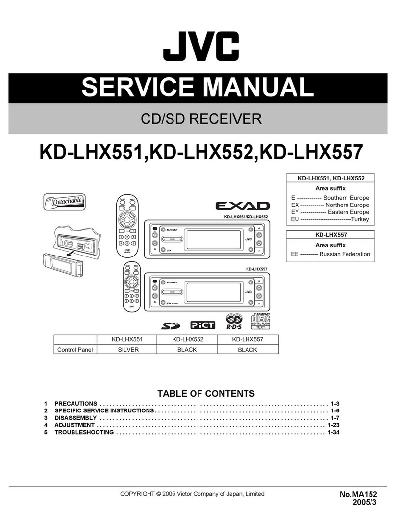
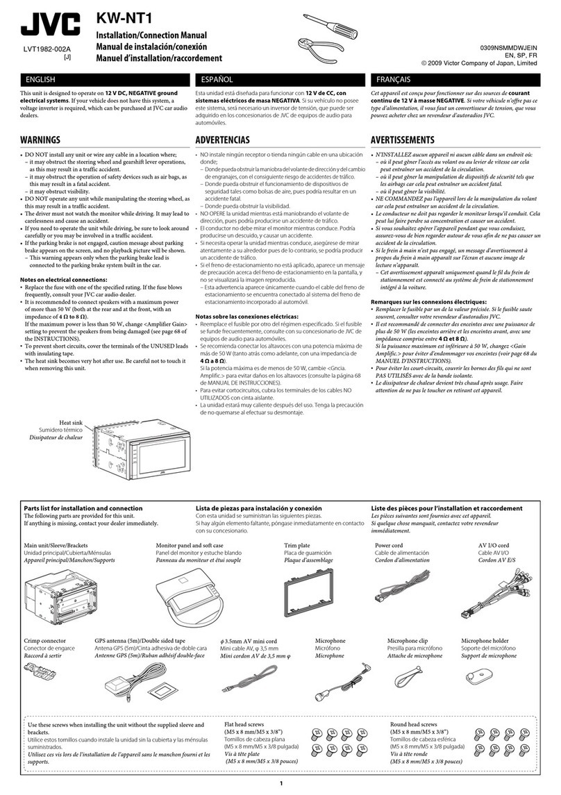
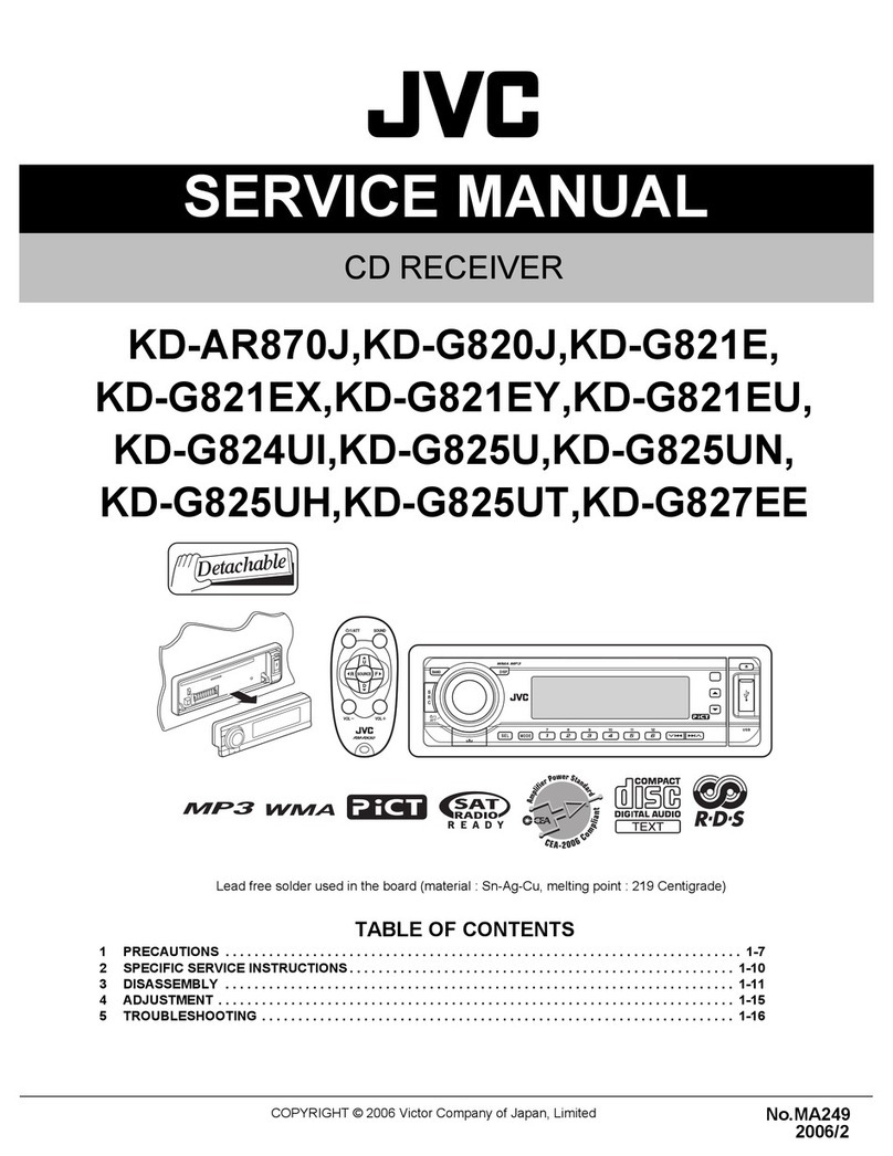
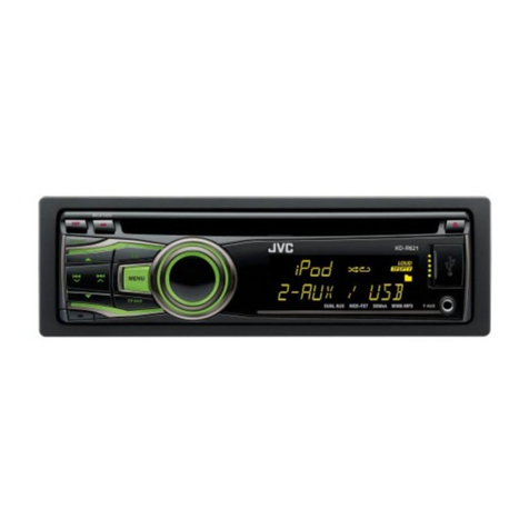
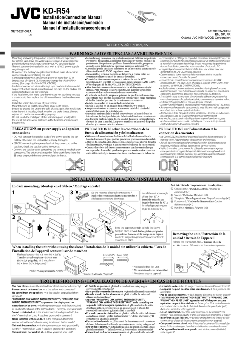
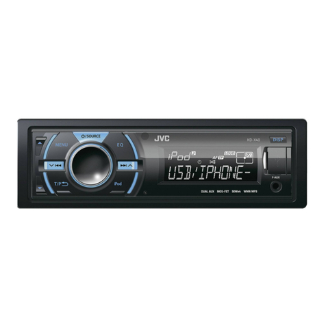
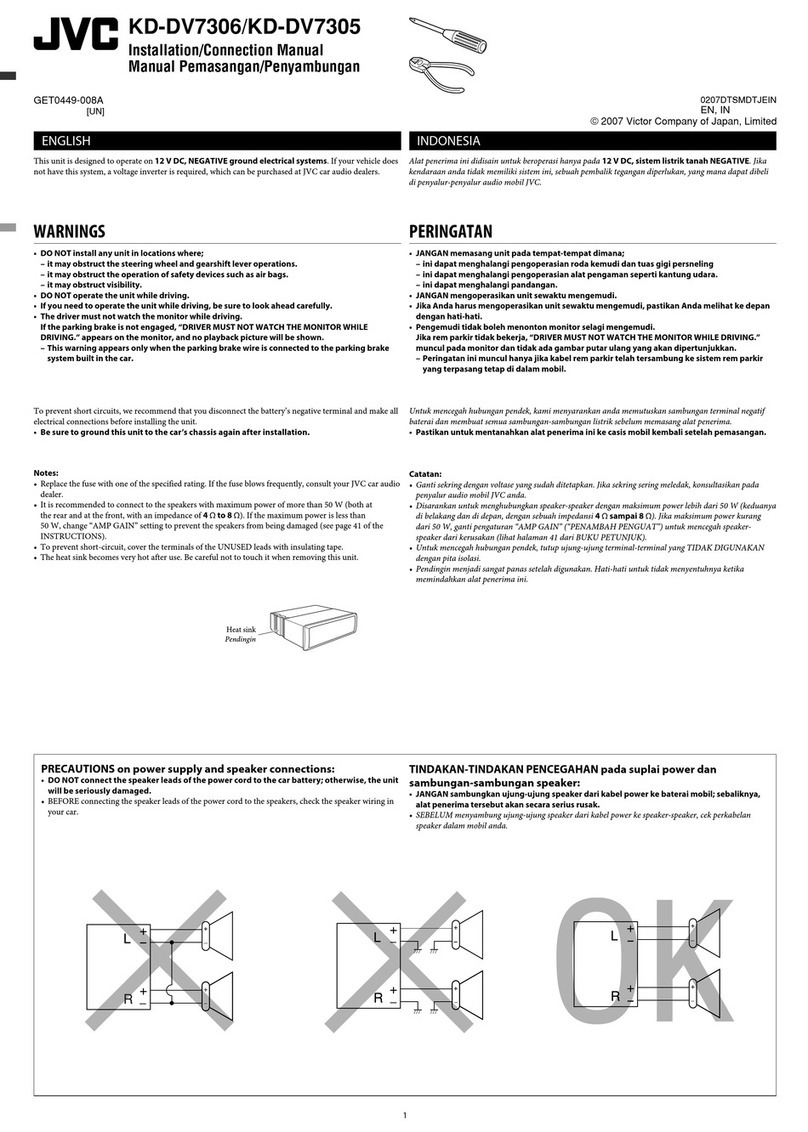
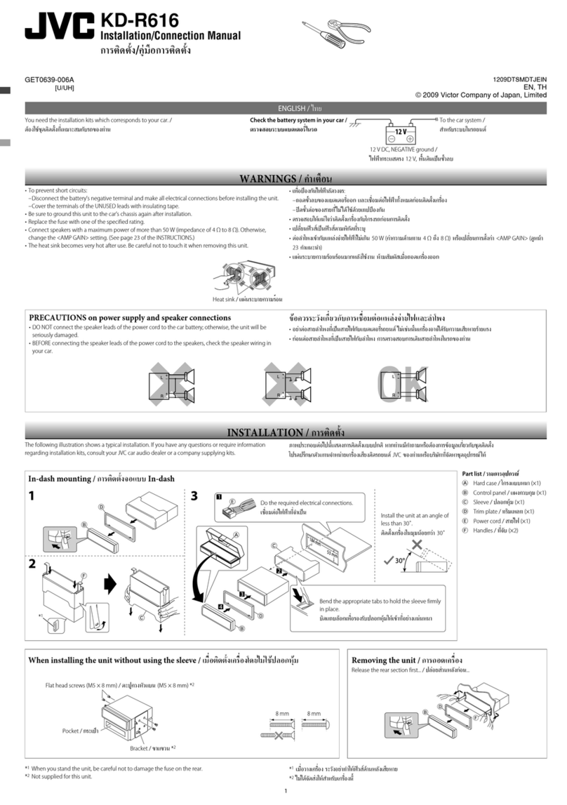
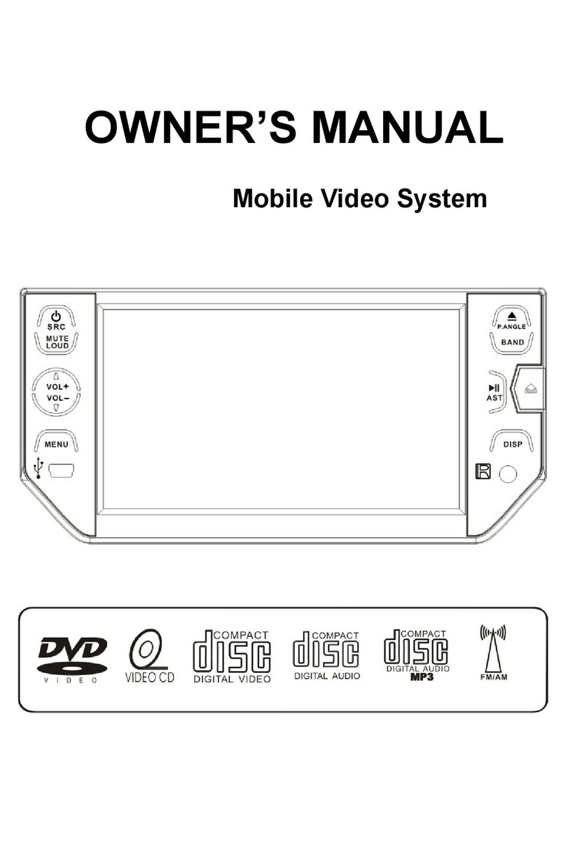
JVC KD-AV7100JW User manual

SERVICE MANUAL
COPYRIGHT © 2008 Victor Company of Japan, Limited No.MA425<Rev.001>
2008/12
DVD RECEIVER WITH MONITOR
MA425<Rev.001>200812SERVICE MANUAL
KD-AV7100JW, KD-AV7100EU,
KD-AV7100EE, KD-AV7100U,
KD-AV7100US, KD-AV7100A
COPYRIGHT © 2008 Victor Company of Japan, Limited
Lead free solder used in the board (material : Sn-Cu, melting point : 230 Centigrade)
TABLE OF CONTENTS
1 PRECAUTION. . . . . . . . . . . . . . . . . . . . . . . . . . . . . . . . . . . . . . . . . . . . . . . . . . . . . . . . . . . . . . . . . . . . . . . . . 1-4
2 SPECIFIC SERVICE INSTRUCTIONS . . . . . . . . . . . . . . . . . . . . . . . . . . . . . . . . . . . . . . . . . . . . . . . . . . . . . . 1-6
3 DISASSEMBLY . . . . . . . . . . . . . . . . . . . . . . . . . . . . . . . . . . . . . . . . . . . . . . . . . . . . . . . . . . . . . . . . . . . . . . . 1-7
4 ADJUSTMENT . . . . . . . . . . . . . . . . . . . . . . . . . . . . . . . . . . . . . . . . . . . . . . . . . . . . . . . . . . . . . . . . . . . . . . . 1-11
5 TROUBLESHOOTING . . . . . . . . . . . . . . . . . . . . . . . . . . . . . . . . . . . . . . . . . . . . . . . . . . . . . . . . . . . . . . . . . 1-14

1-2 (No.MA425<Rev.001>)
SPECIFICATION
AMPLIFIER
Maximum Power Output Front/Rear 50 W per channel
Continuous Power Output (RMS) Front/Rear 20 W per channel into 4 Ω, 40 Hz to 20 000 Hz at no more
than 0.8% total harmonic distortion
Load Impedance 4 Ω(4 Ωto 8 Ωallowance)
Tone Control Range Bass ±14 dB (60 Hz, 80 Hz, 100 Hz, 200 Hz)
Treble ±14 dB (10 kHz, 12.5 kHz, 15 kHz, 17 kHz)
Q (Q-slope) Q1.0, Q1.25, Q1.5, Q2.0
Signal-to-Noise Ratio 70 dB
Audio Output Level FRONT/
REAR/ CENTER/ SUB WOOFER
Line-Out Level/Impedance 4.0 V/20 kΩload (full scale)
Output Impedance 1 kΩ
Color System NTSC/PAL*1
for Spanish NTSC
Video Output (composite) 1 Vp-p/75Ω
Other Terminals Input AV IN, CAMERA, AUX (auxiliary) input jack, USB input
terminal, Aerial input
Output AV OUT
Others iPod, OE REMOTE*2
FM/AM TUNER
Frequency Range USA FM 87.5 MHz - 107.9 MHz/200 kHz
AM 530 kHz - 1 710 kHz/10 kHz
S-Amer1 FM 87.5 MHz - 107.9 MHz/100 kHz
AM 530 kHz - 1 710 kHz/10 kHz
Europe FM 87.50 MHz - 108.00 MHz/50 kHz
AM 522 kHz - 1 620 kHz/9 kHz
Other FM 87.50 MHz - 108.00 MHz/50 kHz
AM 531 kHz - 1 602 kHz/9 kHz
FM Tuner Usable Sensitivity 11.3 dBf (1.0 µV/75 Ω)
50 dB Quieting Sensitivity 16.3 dBf (1.8 µV/75 Ω)
Alternate Channel Selectivity (400 kHz) 65 dB
Frequency Response 40 Hz to 15 000 Hz
Stereo Separation 35 dB
AM Tuner Sensitivity/Selectivity 20 µV/35 dB
DVD/CD
Signal Detection System Non-contact optical pickup (semiconductor laser)
Frequency Response DVD, fs=48 kHz 16 Hz to 22 000 Hz
VCD/CD 16 Hz to 20 000 Hz
Dynamic Range 93 dB
Signal-to-Noise Ratio 95 dB
Wow and Flutter Less than measurable limit
(No.MA425<Rev.001>)1-3
*1 Use an external monitor which can switch the color system (NTSC/PAL) automatically. ( A, EU/US, U, EE )
*2 Not used for this unit. ( A, EU/US, U, JW )
Design and specifications are subject to change without notice.
SD
Compatible File System FAT 32
Capacity 2 Gbytes
Data Transfer Rate Maximum 10 Mbps
USB
USB Standards USB 1.1
Data Transfer Rate Full Speed: Maximum 12 Mbytes
Low Speed: Maximum 1.5 Mbytes
Compatible Device Mass storage class
Compatible File System FAT 32/16/12
Max. Current Less than 500 mA/5 V
MONITOR
Screen Size 7 inch wide liquid crystal display
Number of Pixel 336 960 pixels: 480 x 3 (horizontal) ×234 (vertical)
Drive Method TFT (Thin Film Transistor) active matrix format
Color System NTSC/PAL
for Spanish NTSC
Aspect Ratio 16:9 (wide)
GENERAL
Power Requirement Operating Voltage DC 14.4 V (11 V to 16 V allowance)
Grounding System Negative ground
Allowable Storage Temperature -10°C to +60°C
Allowable Operating Temperature 0°C to +50°C
Dimensions (W ×H ×D):
With trim plate and sleeve at-
tached
Installation Size (approx.) 182 mm ×53 mm ×159 mm
Panel Size (approx.) 188 mm ×58 mm ×13 mm
Detachable Panel Size (approx.) 134 mm ×22 mm ×19 mm
Mass (approx.) 2.5 kg (including trims and sleeve)

1-4 (No.MA425<Rev.001>)
SECTION 1
PRECAUTION
1.1 Safety Precautions
1.2 Preventing static electricity
Electrostatic discharge (ESD), which occurs when static electricity stored in the body, fabric, etc. is discharged, can destroy the laser
diode in the traverse unit (optical pickup). Take care to prevent this when performing repairs.
1.2.1 Grounding to prevent damage by static electricity
Static electricity in the work area can destroy the optical pickup (laser diode) in devices such as CD players.
Be careful to use proper grounding in the area where repairs are being performed.
(1) Ground the workbench
Ground the workbench by laying conductive material (such as a conductive sheet) or an iron plate over it before placing the
traverse unit (optical pickup) on it.
(2) Ground yourself
Use an anti-static wrist strap to release any static electricity built up in your body.
(3) Handling the optical pickup
• In order to maintain quality during transport and before installation, both sides of the laser diode on the replacement optical
pickup are shorted. After replacement, return the shorted parts to their original condition.
(Refer to the text.)
• Do not use a tester to check the condition of the laser diode in the optical pickup. The tester's internal power source can easily
destroy the laser diode.
1.3 Handling the traverse unit (optical pickup)
(1) Do not subject the traverse unit (optical pickup) to strong shocks, as it is a sensitive, complex unit.
(2) Cut off the shorted part of the flexible cable using nippers, etc. after replacing the optical pickup. For specific details, refer to the
replacement procedure in the text. Remove the anti-static pin when replacing the traverse unit. Be careful not to take too long a
time when attaching it to the connector.
(3) Handle the flexible cable carefully as it may break when subjected to strong force.
(4) It is not possible to adjust the semi-fixed resistor that adjusts the laser power. Do not turn it.
!Burrs formed during molding may be left over on some parts of the chassis. Therefore,
pay attention to such burrs in the case of preforming repair of this system.
!Please use enough caution not to see the beam directly or touch it in case of an
adjustment or operation check.
1M
(caption)
Anti-static wrist strap
Conductive material
(conductive sheet) or iron plate

(No.MA425<Rev.001>)1-5
1.4 Important for laser products
1.CLASS 1 LASER PRODUCT
2.CAUTION :
(For U.S.A.) Visible and/or invisible class II laser radiation
when open. Do not stare into beam.
(Others) Visible and/or invisible class 1M laser radiation
when open. Do not view directly with optical instruments.
3.CAUTION : Visible and/or invisible laser radiation when
open and inter lock failed or defeated. Avoid direct
exposure to beam.
4.CAUTION : This laser product uses visible and/or invisible
laser radiation and is equipped with safety switches which
prevent emission of radiation when the drawer is open and
the safety interlocks have failed or are defeated. It is
dangerous to defeat the safety switches.
5.CAUTION : If safety switches malfunction, the laser is able
to function.
6.CAUTION : Use of controls, adjustments or performance of
procedures other than those specified here in may result in
hazardous radiation exposure.
REPRODUCTION AND POSITION OF LABELS and PRINT
!Please use enough caution not to
see the beam directly or touch it
in case of an adjustment or operation
check.
WARNING LABEL and PRINT

1-6 (No.MA425<Rev.001>)
SECTION 2
SPECIFIC SERVICE INSTRUCTIONS
This service manual does not describe SPECIFIC SERVICE INSTRUCTIONS.

(No.MA425<Rev.001>)1-7
SECTION 3
DISASSEMBLY
3.1 Main body (Used figure are KD-AV7100E)
3.1.1 Removing the Top chassis (See Fig.1 to 7)
(1) Remove the two screws Aattaching the FPC cover. (See
Fig.1)
(2) Disconnect the FPC wire connected to connector CON11
and CON19 of the Main board. (See Fig.2)
(3) Remove the two screws Battaching the Top chassis. (See
Fig.3)
(4) Remove the four screws Cattaching the both side of the
Top chassis. (See Fig.4)
(5) Remove the two screws Dattaching the both side of the
Front chassis. (See Fig.4)
(6) Disengage two hooks aengaged both side of the Front
chassis. (See Fig.5)
(7) Disconnect the connector wire from Front chassis connect-
ed to connector CON2 of the USB board. (See Fig.6)
(8) Tear off an FPC from a CD mechanism and then remove
the Top chassis. (See Fig.7)
Fig.1
Fig.2
Fig.3
Fig.4
Fig.5
Fig.6
Fig.7
A
FPC cove
r
CON11
CON19
B
C
D
hook a
CON2
FPC

1-8 (No.MA425<Rev.001>)
3.1.2 Removing the USB board (See Fig.8)
(1) Disconnect the connector wire from Main board connected
to connector CON1 of the USB board.
(2) Remove the two screws Eattaching the USB board.
Fig.8
3.1.3 Removing the CD mechanism (See Fig.9, 10)
(1) Remove the four screws Fattaching the CD mechanism.
(See Fig.9)
(2) Disconnect the FPC from CD mechanism connected to
connector CON16 of the Main board. (See Fig.10)
Fig.9
Fig.10
3.1.4 Removing the Main board (See Fig.11 to 13)
(1) Remove the Signal cables from Bottom chassis. (See
Fig.11)
(2) Remove the two screws Gattaching the FAN. (See Fig.11)
(3) Remove the two screws Hattaching the FAN cover. (See
Fig.11)
(4) Remove the two screws Jattaching the Heat sink with IC
bracket. (See Fig.12)
(5) Remove the two screws Kattaching the Main board. (See
Fig.13)
Fig.11
Fig.12
Fig.13
CON1
USB board
E
FF
CON16
CD mechanism FPC
Signal cables
FAN cover
G
HH
JHeat sink
IC bracket inside
Main board
K

(No.MA425<Rev.001>)1-9
3.1.5 Removing the Key board (See Fig.14)
(1) Remove the Volume knob.
(2) Remove the six screws Lattaching the Rear cover.
Fig.14
3.1.6 Removing the LCD monitor (See Fig.15 to 18)
There are two ways of methods to exclude monitor block.
Method 1: Press [OPEN] button.
Method 2: After remove the Top chassis, supply voltage approx
3.0V to Motor (See Fig.15)
(1) Remove the two screws Mattaching the FPC cover. (See
Fig.16)
(2) Remove the two screws Nand two screws Pattaching the
L panel cover. (See Fig.16)
(3) Disconnect the FPC from drive unit connected to connector
CON1 of the TFT board. (See Fig.17)
(4) Remove the six screws Qattaching the both side of the
Screen panel. (See Fig.18)
Fig.15
Fig.16
Fig.17
Fig.18
L
L
Motorapprox 3.0V
MM
N
PP
N
L panel cover
FPC cover
CON1
FPC
Q

1-10 (No.MA425<Rev.001>)
3.1.7 Removing the TFT board (See Fig.19)
(1) Disconnect the FPC from LCD connected to connector
CON2 and CON4 of the TFT board.
(2) Disconnect the card wire from LCD board connected to
connector CON7404 of the TFT board.
(3) Disconnect the card wire from CCLF board connected to
connector CON5 of the TFT board.
(4) Disconnect the FPC from LCD lens connected to connector
CON20 of the TFT board.
(5) Remove the two screws Rattaching the PCB bracket.
(6) Remove the three screws Sattaching the PCB bracket.
Fig.19
3.1.8 Removing the CCLF board (See Fig.20)
(1) Disconnect the connector wire from LCD lens connected to
connector CON102 of the CCLF board.
(2) Remove the one screw Tattaching the CCLF board.
Fig.20
R
S
SS
R
PCB bracket
PCB bracket
CON2
CON5
CON4
CON7404
CON20
CON102CCLF board
LCD lens
T

(No.MA425<Rev.001>)1-11
SECTION 4
ADJUSTMENT
4.1 ADJUSTMENT
4.1.1 Test instruments required for adjustment
(1) Digital oscilloscope (100MHz)
(2) Digital tester
(3) Test Disc
(4) Extension cable : EXTAV70X-50PF
4.1.2 Standard volume position
Balance and Bass &Treble volume : lndication"0"
Loudness : OFF
4.1.3 Standard measuring conditions
Power supply voltage DC14.4V(10.5 to 16V)
Load impedance 20K ohm (2 Speakers connection)
Output Level Line out 2.5V (Vol. MAX)
4.1.4 Dummy load
Exclusive dummy load should be used for AM,and FM. For FM
dummy load,there is a loss of 6dB between SSG output and an-
tenna input.The loss of 6dB need not be considered since direct
reading of figures are applied in this working standard.
4.1.5 How to connect the extension cable for adjusting
Be sure to attach the heat sink and rear bracket onto the power amplifier IC and regulator IC respectively, before supply the power.
If voltage is applied without attaching these parts, the power amplifier IC and regulator IC will be destroyed by heat.
Extension cable
EXTAV70X-50PF

1-12 (No.MA425<Rev.001>)
4.1.6 Service mode
• When adjusting, switch on the main unit and insert a test disc (VT-501). And play the test disc and pause it.
(1) Power ON
(2) Use the remote controller (RM-RK253).
(3) Push the button of remote controller with the following order.
[SRC] button →[ 1 ] button →[ 2 ] button
(4) Exchanging it operate a menu of a service mode with the [ ] button and [ ] button.
(5) Change data with the [ ]/[ ] buttons.
(6) Write data with a [INFO ] button of the main body.
Indication Minimum value Maximum
value
Reference
register value
Detail
1 Data - - - - Only factory use
2 Version - - - - Only factory use
3 Sch - - - - Only factory use
4 Pcb - - - - Only factory use
5 KeyCode - - - - Only factory use
6 Counter - - - - Only factory use
7 Count MSB - - - - Only factory use
8 Count LSB - - - - Only factory use
9 FM LOC *1 00 FF 40 Adjust STOP sensitivity adjustment of FM LOC mode
10 AM LOC 00 FF A0 Adjust STOP sensitivity adjustment of AM LOC mode No use
11 FM DX *1 00 FF 40 Adjust STOP sensitivity adjustment of FM DX mode
12 AM DX *1 00 FF 50 Adjust STOP sensitivity adjustment of AM DX mode
17 CTRST 00 7F 60 Adjust Contrast control
Power save
18 CLOR 80 FF A0 Adjust Color control
Chroma trap filter for Y input
19 TINT 00 FF A0 Adjust Tint control (Base Band TINT)
RGB input coupling mode
20 SHAP 00 FF 30 Adjust Comb filter for base-band color signal of NTSC
CW out mode
Sharpness control
21 BRT 00 FF 98 Adjust Brightness control
22 SUBC 00 FF 60 Adjust Auto Brightness Limiter start point
Auto Brightness Limiter off
Auto Brightness Limiter Gain
Controls the Y amplitude
23 W/BLIM 00 FF FA Adjust White clipping voltage for RGB signal exceeding over white
Limit voltage for RGB signal exceeding below black
24 GM1 10 FF A8 Adjust Correction peak point
25 GM2 10 FF 50 Adjust Boost gain correction peak point
26 SUBT-RB 00 FF A8 Adjust Sub brightness control for R output singal
Sub brightness control for B output signal
27 DRVR 00 FF 1A Adjust Mute switch for RGB output signal
Insert fixed level blue signal for RGB output
Gain control for R video signal
28 DRVG 00 FF 18 Adjust Relative amplitude of R-Y color difference signal
Relative phase of R-Y color difference signal
Gain control for G video signal
29 DRVB 00 FF 18 Adjust Relative amplitude of G-Y color difference signal
Relative phase of G-Y color difference signal
Gain control for B video signal

(No.MA425<Rev.001>)1-13
*1 Seek stop sensitivity SSG setting
FM
AM
30 V-SW 00 FF AA Adjust Synchronization mode
Polarity cobtrol for the WIDEBLK input signal
Video switch
31 COMA 00 FF A3 Adjust Common Pulse Amplitude
32 COMDC 00 FF 26 Adjust Reference DC output
33 VFRE 00 FF 00 Fix Force Dotclk for T-Con stopping
AFC2 Phase control
Driving ability of pulse output stage
34 SINHI 00 FF 00 Fix SECAM Inhibit
Low pass filter for Y input
Dot clock PLL
Polarity switch of video signal inverter
Polarity switch of common pulse inverter
35 PDCK 00 FF A7 Fix Polarity control for Compare Pulse input signal
Polarity control for VD output signal
Polarity control for HD output signal
Control the Divider for the Dot clock output signal
DOTCLK adjustment
36 PADJ 10 FF 20 Fix VD phase phase
DOTCLK adjustment
37 VPHASE 00 07 00 Adjust VD out Phase
37 HPHASE 00 1F 11 Adjust HD out Phase
38 GM2RGB 00 FF 00 Adjust Gamma2 Gain extension for R,G,B
39 T1 00 FF 00 Fix For IC testing at plant
40 T2 00 FF 00 Fix For IC testing at plant
41 SID_S 00 FF 02 Fix SECAM Gate pulse phase
SECAM ID sensitivity
SECAM ID mode
Enhance the higher side of SECAM Bell filter
PAL/NTSC ID sensitivity for digital comb filter
Select chroma BPF frequency response
ABCL SW
42 S_BLK 10 FF 88 Fix R-Y Black level adjust for SECAM
B-Y Black level adjust for SECAM
97.9MHz or 98.1MHz LOC: 33dBuV (min.) 43dBuV (max.) 38dBuV (normal)
400Hz (sig.) 22.5kHz (Dev.) DX : 18dBuV (min.) 28dBuV (max.) 23dBuV (normal)
Indication Minimum value Maximum
value
Reference
register value
Detail
999kHz or 1000kHz 24dBuV (min.) 34dBuV (max.) 29dBuV (noemal)
400Hz (Sig.) 30%

1-14 (No.MA425<Rev.001>)
SECTION 5
TROUBLESHOOTING
5.1 16 PIN CORD DIAGRAM (for JW,U,A)
YL
WH/BK
RD
VI
BK
VI/BK
GY
11
1
13
4
16
12
3
VI/WH
5
WH/BK
10 GN
9GN/BK
GY/BK
OR/WH
15
14
7
BL/WH
Black
RD
BK
Red
BL
Blue
WH
White
GN
Green
GY
Gray
Yellow
VI
Violet
YL
Orange
OR
9
10
11
12
8
7
5
13
14
15
16
4
3
2
1
BK
RD
WH
GN
VI GY
BL/WH
GN/BK
VI/WH
GY/BK
YL
BL
WH/BK
NC 6
OR/WH
VI/BK
2WH
8

(No.MA425<Rev.001>)1-15
5.2 16 PIN CORD DIAGRAM (for EU,EE,US)
YL
BR
RD
VI
BK
VI/BK
GY
11
6
1
8
2
4
16
12
WH
3
VI/WH
5
WH/BK
10 GN
9GN/BK
GY/BK
OR/WH
15
14
7
BL/WH
9
10
11
12
8
7
5
13
14
15
16
4
3
2
1
BK
RD
WH
GN
VI GY
BL/WH
GN/BK
VI/WH
GY/BK
YL
NC
WH/BK
BR 6
OR/WH
VI/BK
1
3
5
7
2
4
6
8
NC
BL/WH
YL
RD BK
NC BR
OR/WH
Black
RD
BK
Red
BL
Blue
WH
White
GN
Green
GY
Gray
Yellow
VI
Violet
YL
Brown
BR
Orange
OR
1
3
5
7
2
4
6
8
GY
WH
GY/BK
GN
GN/BK
VI
VI/BK
WH/BK

(No.MA425<Rev.001>)
VPT
Printed in Japan
Victor Company of Japan, Limited
Mobile Entertainment Division 10-1,1chome,Ohwatari-machi,Maebashi-city,371-8543,Japan
This manual suits for next models
5
Table of contents
Other JVC Car Receiver manuals