KV-DV7
1-3
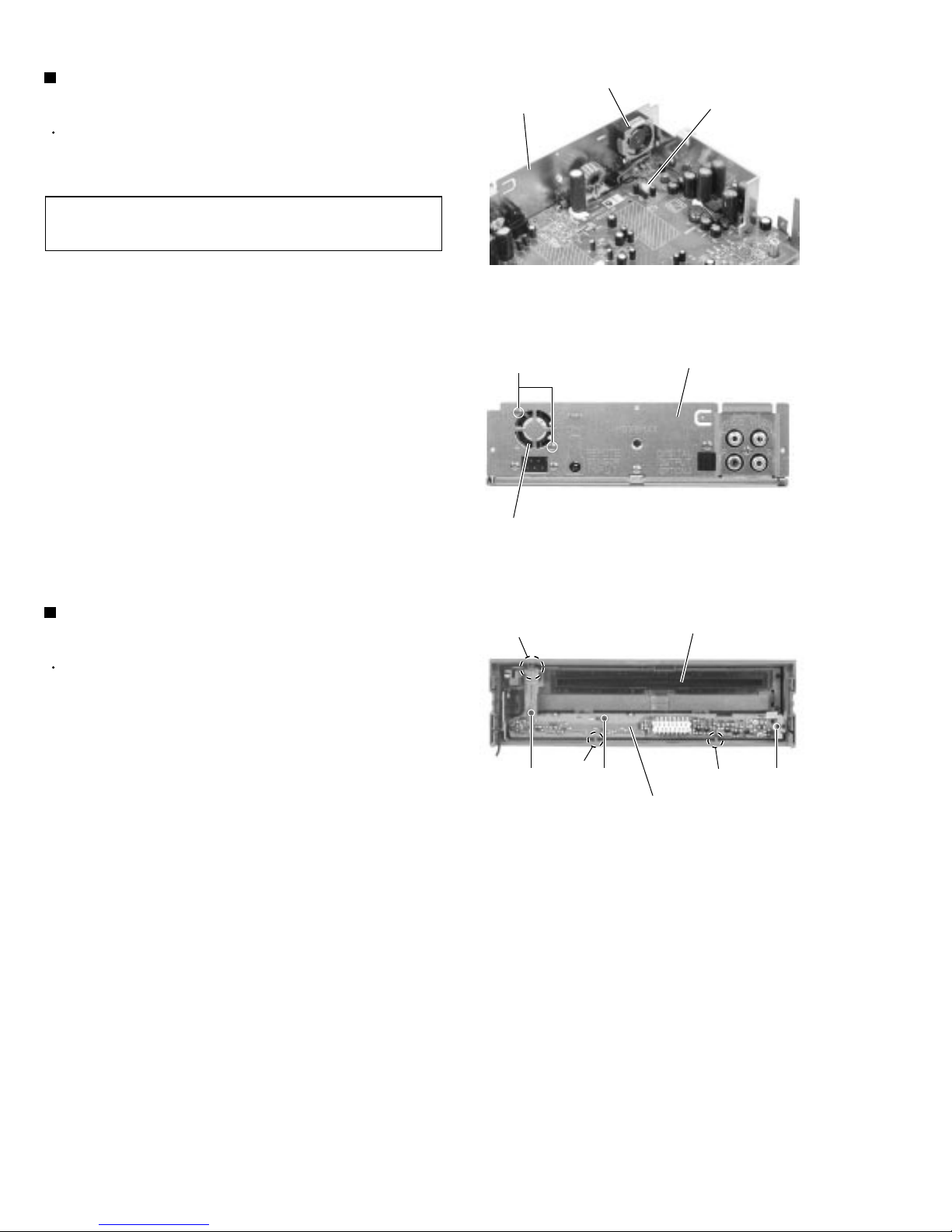
Important for laser products
1.CLASS 1 LASER PRODUCT
2.DANGER : Invisible laser radiation when open and inter
lock failed or defeated. Avoid direct exposure to beam.
3.CAUTION : There are no serviceable parts inside the
Laser Unit. Do not disassemble the Laser Unit. Replace
the complete Laser Unit if it malfunctions.
4.CAUTION : The compact disc player uses invisible
laserradiation and is equipped with safety switches
whichprevent emission of radiation when the drawer is
open and the safety interlocks have failed or are de
feated. It is dangerous to defeat the safety switches.
5.CAUTION : If safety switches malfunction, the laser is able
to function.
6.CAUTION : Use of controls, adjustments or performance of
procedures other than those specified herein may result in
hazardous radiation exposure.
VARNING : Osynlig laserstrålning är denna del är öppnad
och spårren är urkopplad. Betrakta ej strålen.
VARO : Avattaessa ja suojalukitus ohitettaessa olet
alttiina näkymättömälle lasersäteilylle.Älä katso
säteeseen.
ADVARSEL : Usynlig laserstråling ved åbning , når
sikkerhedsafbrydere er ude af funktion. Undgå
udsættelse for stråling.
ADVARSEL : Usynlig laserstråling ved åpning,når
sikkerhetsbryteren er avslott. unngå utsettelse
for stråling.
REPRODUCTION AND POSITION OF LABELS
WARNING LABEL
!
CAUTION
Please use enough caution not to
see the beam directly or touch it
in case of an adjustment or operation
check.
CLASS 1
LASER PRODUCT
DANGER : Invisibie laser radiation
when open and interlock or
defeated.
AVOID DIRECT EXPOSURE TO
BEAM (e)
VARNING : Osynlig laserstrålning är
denna del är öppnad och spårren är
urkopplad. Betrakta ej strålen. (s)
VARO : Avattaessa ja suojalukitus
ohitettaessa olet alttiina
näkymättömälle lasersäteilylle.Älä
katso säteeseen. (d)
ADVARSEL :Usynlig laserstråling
ved åbning , når
sikkerhedsafbrydere er ude af
funktion. Undgå udsættelse for
stråling. (f)