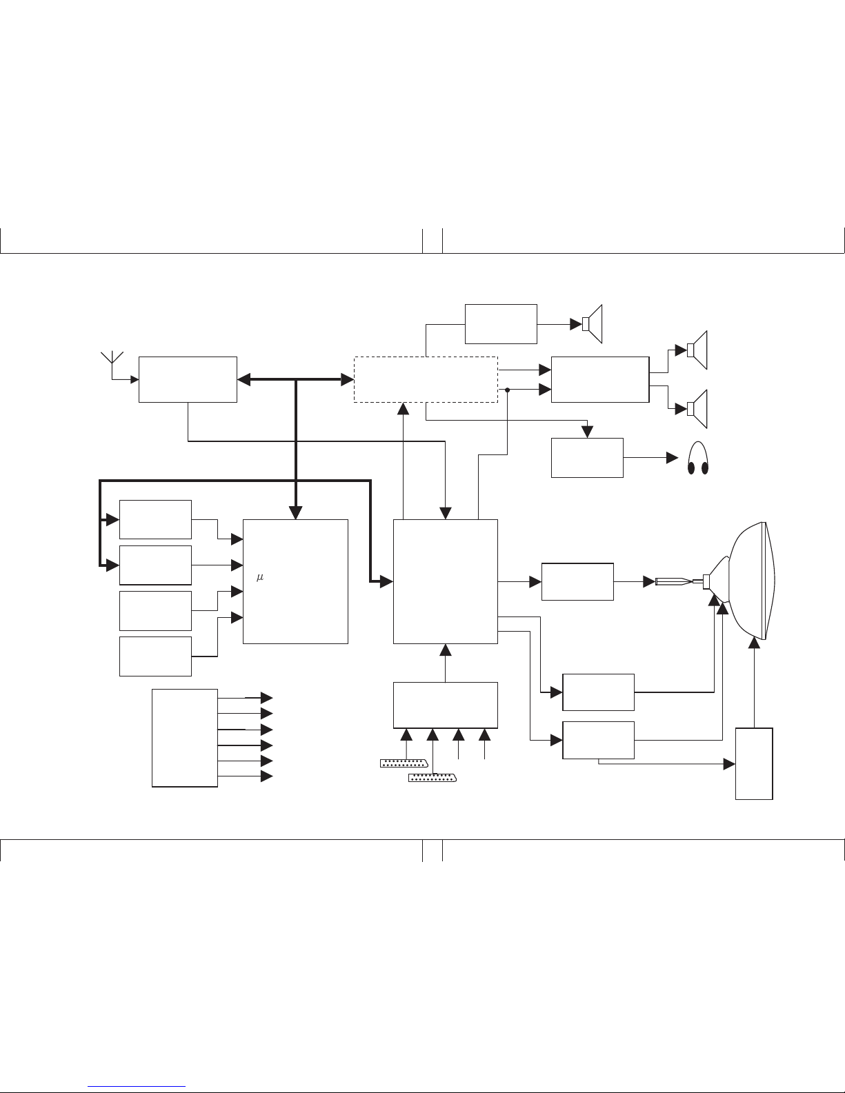
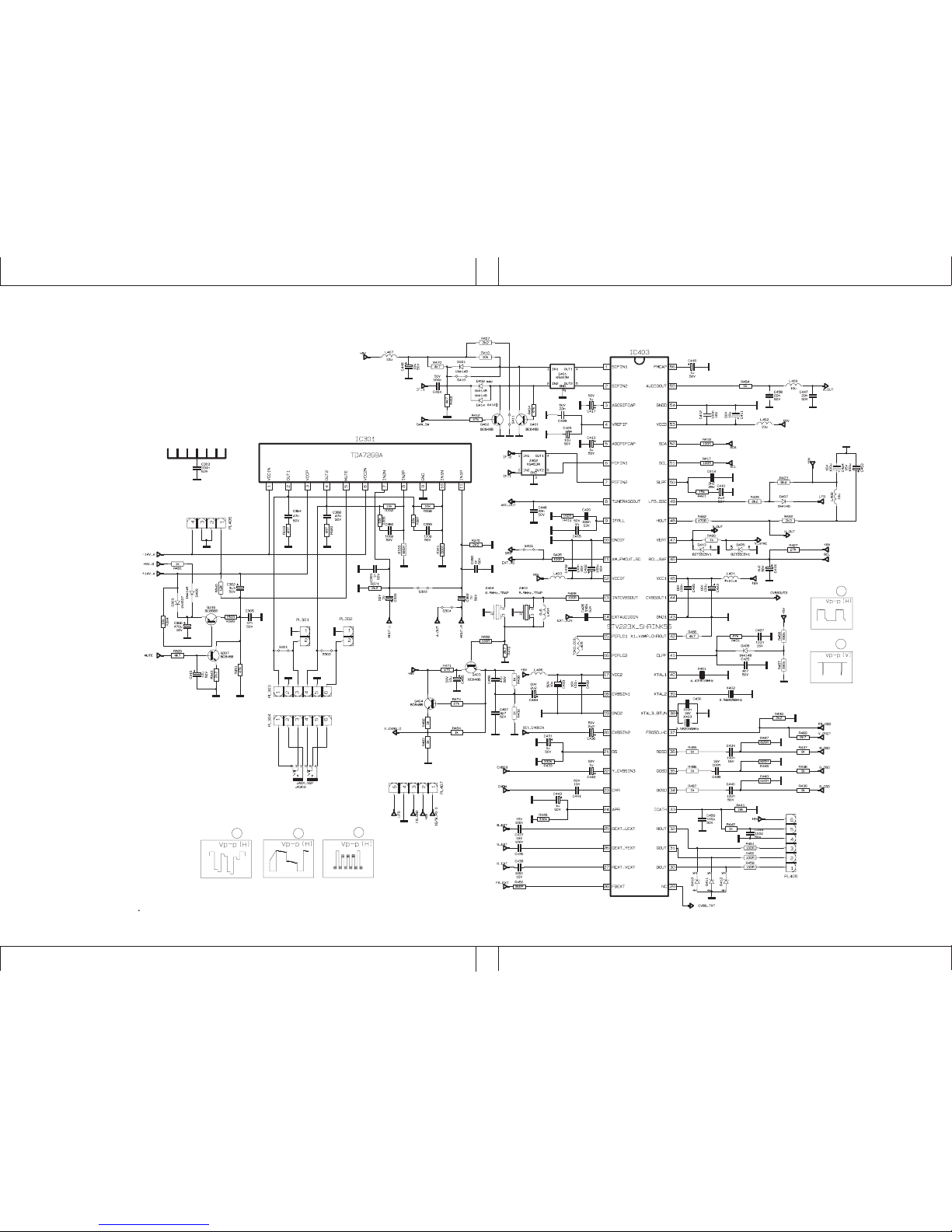
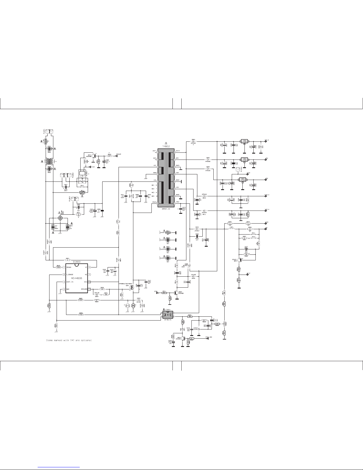
STANDARD CIRCUIT DIAGRAM
NOTE ON USING CIRCUIT DIAGRAMS
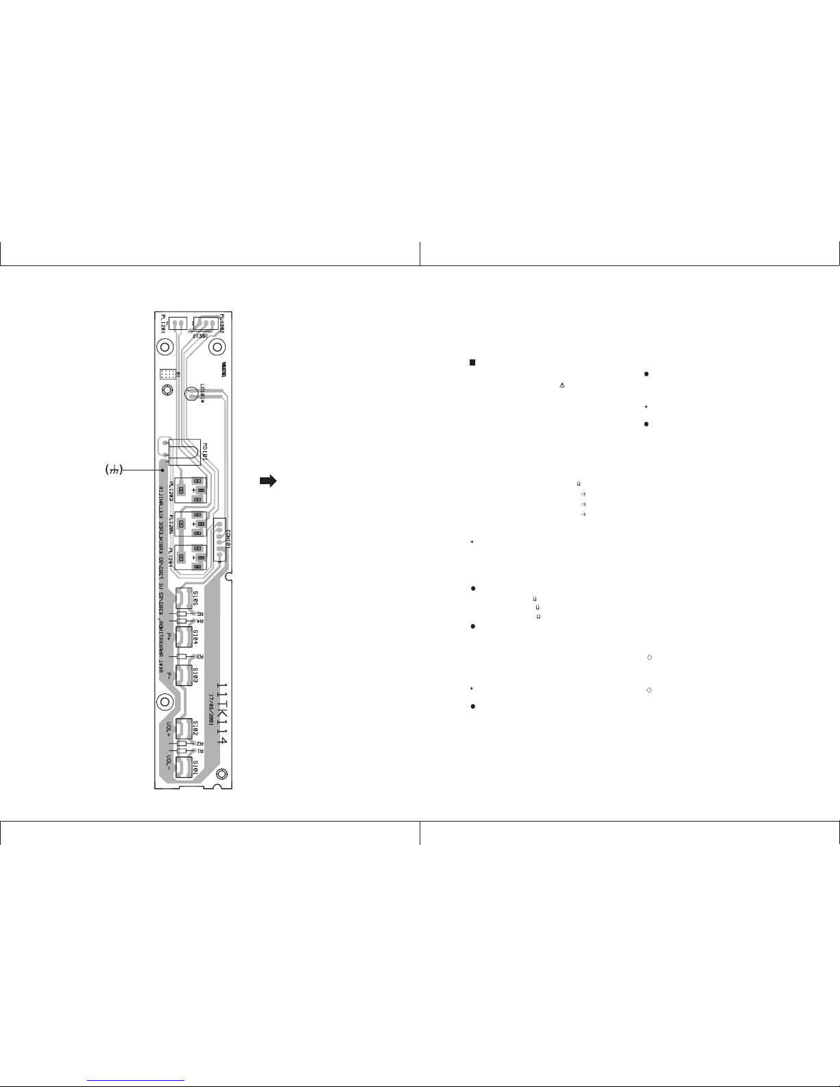
1.SAFETY
The components identified by the symbol and shading are
critical for safety. For continued safety replace safety critical
components only with manufactures recommended parts.
2.SPECIFIED VOLTAGE AND WAVEFORM VALUES
The voltage and waveform values have been measured under the
following conditions.
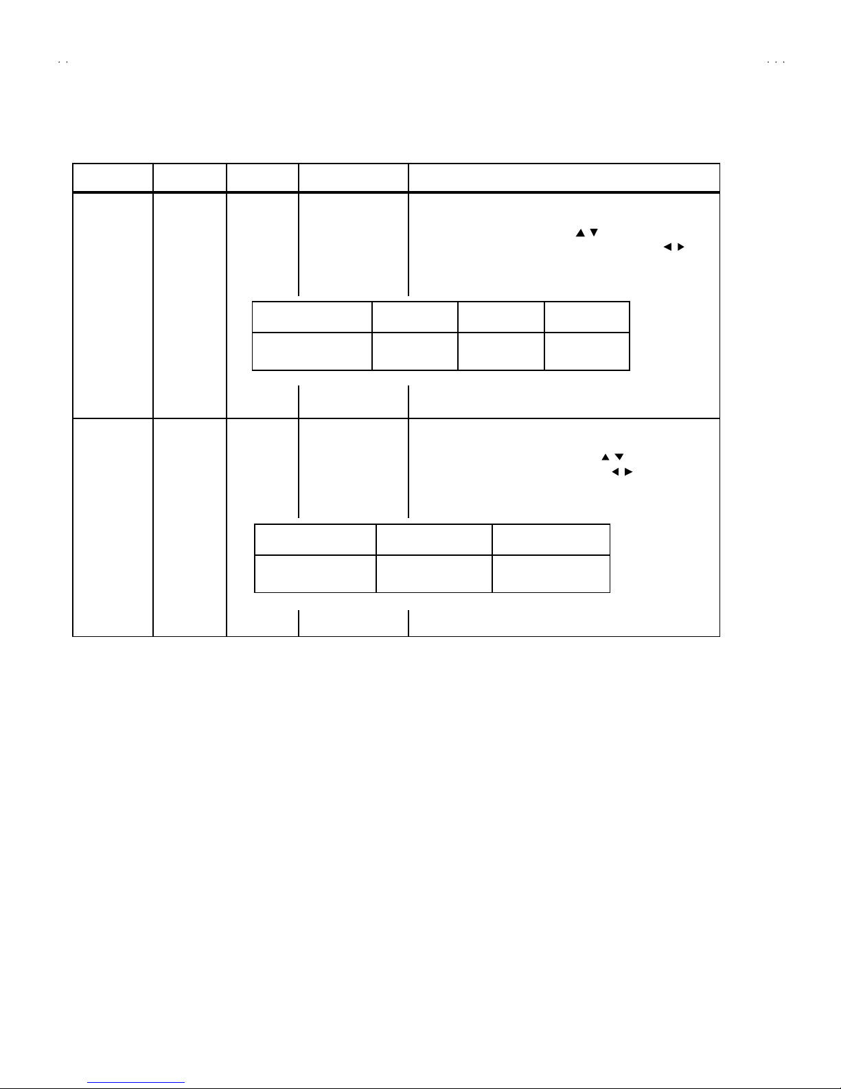
(1)Input signal : Colour bar signal
(2)Setting positions of
each knob/button and
variable resistor
(3)Internal resistance of tester :DC 20k /V
(4)Oscilloscope sweeping time :H 20µS/div
:V 5mS/div
:Others Sweeping time is
specified
(5)Voltage values :All DC voltage values
Since the voltage values of signal circuit vary to some extent
according to adjustments, use them as reference values.
3.INDICATIONS ON THE CIRCUIT DIAGRAM
(1)Resistors
Resistance value
No unit :[ ]
K:[K ]
M
Type
No indication :Carbon resistor
OMR :Oxide metal film resistor
MFR :Metal film resistor
MPR :Metal plate resistor
UNFR :Uninflammable resistor
FR :Fusible resistor
Composition resistor 1/2 [W] is specified as 1/2S or Comp.
(2)Capacitors
: Original setting position
when shipped
4.NOTE FOR REPAIRING SERVICE
This model's power circuit is partly different in the GND. The
difference of the GND is shown by the LIVE side GND and the
ISOLATED(NEUTRAL) side GND.Therefore, care must be
taken for the following points.
(1)Do not touch the LIVE side GND or the LIVE side GND and the
ISOLATED(NEUTRAL) side GND simultaneously. If the above
caution is not respected, an electric shock may be caused.
Therefore, make sure that the power cord is surely removed from
the receptacle when, for example, the chassis is pulled out.
(2)Do not short between the LIVE side GND and ISOLATED(NEUTRAL)
side GND or never measure with a measuring apparatus measure
with a measuring apparatus ( oscilloscope, etc.) the LIVE side GND
and ISOLATED(NEUTRAL) side GND at the same time.
Ifthe aboveprecaution isnot respected ,a fuse or any parts will be broken.
Since the circuit diagram is a standard one, the circuit and
circuit constants may be subject to change for improvement
without any notice.
NOTE
Due improvement in performance, some part numbers show
in the circuit diagram may not agree with those indicated in
the part list.
When ordering parts, please use the numbers that appear
in the Parts List.
Type
MM :Metalized mylar capacitor
PP :Polypropylene capacitor
MPP :Metalized polypropylene capacitor
MF :Metalized film capacitor
TF :Thin film capacitor
BP :Bipolar electrolytic capacitor
TAN :Tantalum capacitor
(3)Coils
No unit :[ µH]
Others :As specified
:[M ]
Capacitance value
1 or higher :[pF]
less than 1 :[µF]
Withstand voltage
No indication :DC50[V]
Others :DC withstand voltage [V]
AC indicated :AC withstand voltage[V]
Electrolytic Capacitors
47/50[Example]:Capacitance value [µF]/withstand voltage[V]
No indication :Ceramic capacitor
AV-25BT6ENS, AV-25BT6ENB