TH-D72A/D72E
7
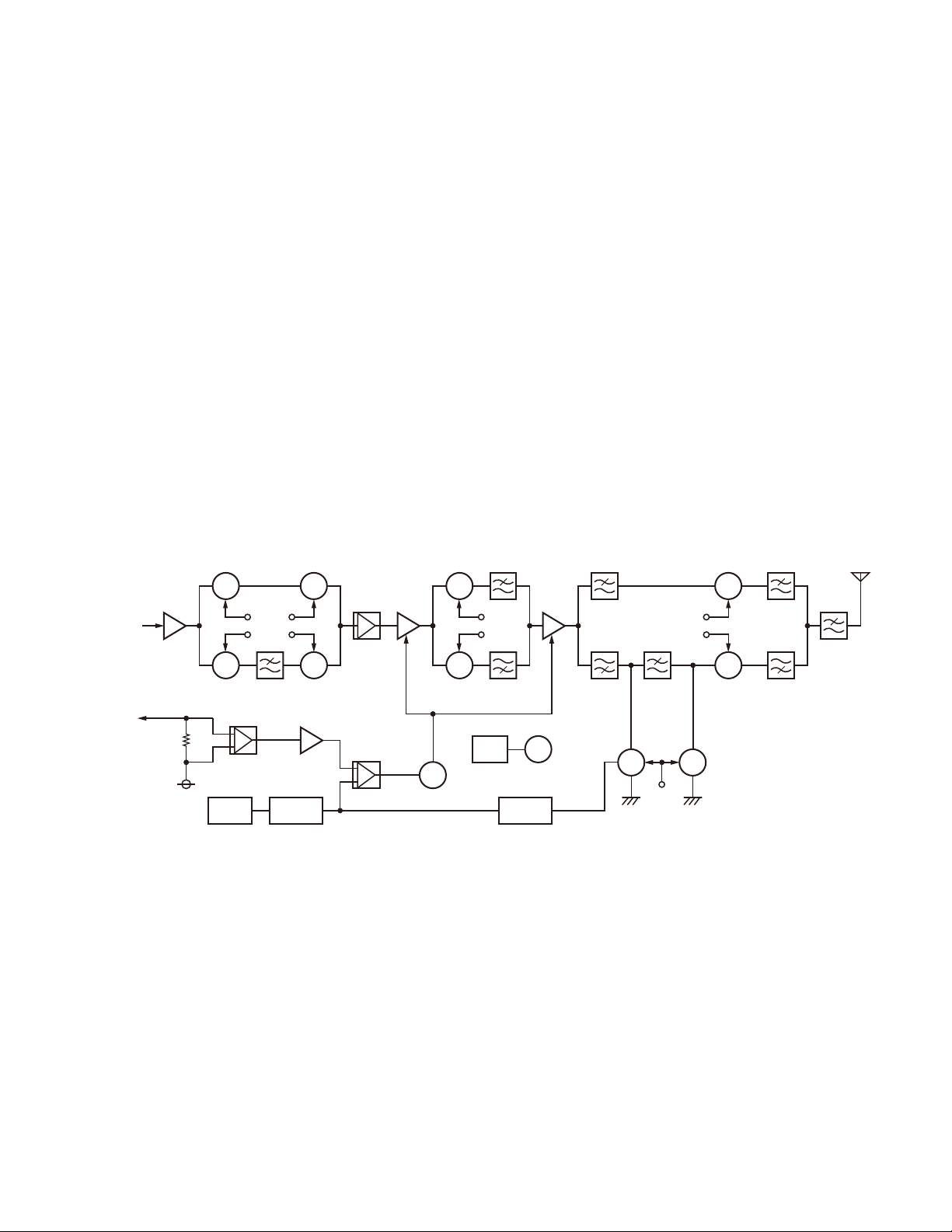
Figure 3 Transmitter circuit
RF
SW RF
SW
RF
SW RF
SW
D201 D204
RF
SW
Q212
D202
Q201
D205
IC202 Q214
VHF
LPF
430T
144T
RF
SW
RF
SW
RF
SW RF
SW
D217
D220,D222
D215,D216
D219,D221
430T
144T
144T
RF
SW
RF
SW
D212
D211
UHF
HPF
UHF
HPF
UHF
LPF
VHF
LPF
VHF
LPF
UHF
HPF
UHF
LPF
VHF
LPF
430T
144T
Q215
IC201 Q207
From
VCO B
To
Q214
Q215 R216
R217 Sub
MCU TH
TH201IC611
–
+IC203
–
+
IC721
E-
Volume
D225,D226
Voltage
shift
IC737
Main
MCU
+B
D214
D223
D227
D228
4. Transmitter System
4-1. Transmitter circuit
The VHF TX signal of the VCO B output through the RF
amplifier (Q201) passes through the band switches (D202,
D205), is amplified with the Pre-drive amplifier (IC202) and
Drive amplifier (Q214), passes through the band switch
(D211) and is amplified to the final output level with the
Final amplifier (Q215). The signal then passes through the
antenna switch (D215, D216), Duplexer and LPF, and is fed
to the antenna.
The UHF TX signal of the VCO B output through the RF
amplifier (Q201) passes through the band switches (D201,
D204), is amplified with the Pre-drive amplifier (IC202) and
Drive amplifier (Q214), passes through the band switch
(D212) and is amplified to the final output level with the
Final amplifier (Q215). The signal then passes through the
antenna switch (D217), Duplexer and LPF, and is fed to the
antenna.
4-2. APC circuit
The Automatic transmission Power Control (APC) is a cir-
cuit to obtain a steady TX Power, and controls the TX Power
detecting the drain current of the Drive amplifier (Q214) and
Final amplifier (Q215). The voltage difference generated by
the drain current in the resisters (R216, R217) is amplified
with the OP-Amplifier (IC201) and DC Amplifier (Q207), and
the detecting voltage is obtained. The control voltage output
from E-volume (IC721) controlled with the Main MCU (IC737)
according to each band and TX Power is prepared. These
two obtained voltages are compared with the OP-Amplifier
(IC203) and obtains the APC voltage. The Gate voltage
of the Drive amplifier (Q214) and Final amplifier (Q215) is
changed depending on this APC voltage and the TX Power
is controlled.
4-3. Thermal protection circuit
The Sub MCU (IC611) observes the detecting voltage
by the Thermistor (TH201) arranged to prevent the thermal
fracture of the Final amplifier (Q215). The APC voltage is
changed when the preset temperature is exceeded, and
excessive generation of heat is prevented by controlling the
TX Power.
5. VCO-PLL Circuit
5-1. Oscillator circuit
The reference frequency (16.800MHz) generated with
the TCXO (X431) of the Band A oscillation circuit is divided
frequency in the PLL IC (IC431) and obtains the comparison
frequencies of 5kHz or 6.25kHz. Similarly, the reference
frequency (16.800MHz) generated with the TCXO (X511) of
the Band B oscillation circuit is divided frequency in the PLL
IC (IC513) and obtains the comparison frequencies of 5kHz
or 6.25kHz. The reference oscillator of Band A generated to
three times with the RF amplifier (Q357) is used also for the
second-local oscillator for the reception of Band A.
The Band A VCO oscillates and is amplified with oscilla-
tion amplifier (Q435), and output to the F-in amplifier (Q434)
and F-out amplifier (Q437) through the Buffer amplifier
(Q436). The Band B VCO oscillates and is amplified with
two oscillation amplifiers (Q522, Q523), and output to the
F-in amplifier (Q521) and F-out amplifier (Q201) through the
Buffer amplifier (Q524). To improve the modulation charac-
teristics of the DCS and 9600bps packet signal, the modula-
tion is put on the TCXO (X431) of Band B.
5-2. Phase comparator
The PLL ICs (IC431, IC513) of the pulse-swallow method
divides the input oscillator frequency and reference fre-
quency according to the PLL Data from the Sub MCU (IC611),
and achieves the PLL synthesizer corresponding to the step
frequency by comparing phases.
CIRCUIT DESCRIPTION


 User manual")


 User manual")