Kenwood NEXEDGE NX-411 User manual

SERVICE MANUAL
This product complies with the RoHS directive for the European market.
© 2011-12 PRINTED IN JAPAN
B53-7002-00 (Y)330
NX-411
900MHz DIGITAL TRANSCEIVER
GENERAL..................................................................2
SYSTEM SET-UP.......................................................3
REALIGNMENT......................................................... 3
INSTALLATION..........................................................6
DISASSEMBLY FOR REPAIR...................................8
CIRCUIT DESCRIPTION .........................................12
COMPONENTS DESCRIPTION..............................19
PARTS LIST............................................................. 21
EXPLODEDVIEW....................................................31
PACKING .................................................................32
TROUBLE SHOOTING............................................33
ADJUSTMENT.........................................................36
TERMINAL FUNCTION ...........................................56
Does not come with antenna. Antenna is available
as an option.
PC BOARD
DISPLAY UNIT (X54-3770-10)............................ 64
TX-RX UNIT (X57-8120-10)................................68
INTERCONNECTION DIAGRAM.............................72
SCHEMATIC DIAGRAM ..........................................74
BLOCK DIAGRAM ..................................................86
LEVEL DIAGRAM ...................................................89
OPTIONAL ACCESSORIES
KNB-32N (Ni-MH Battery Pack) ........................ 90
KNB-33L (Li-ion Battery Pack) .........................90
KNB-54N (Ni-MH Battery Pack) ........................ 90
KSC-32 (Rapid Charger) ...................................90
KBP-6 (Battery Case) ........................................ 90
SPECIFICATIONS....................................................91
CONTENTS
Knob (Selector)
(K29-9305-03)
Knob (Volume)
(K29-9304-03)
Main cabinet (18 key)
(A02-4076-11)
Whip antenna
(KRA-38: option)
Badge
(B43-1606-04)
Knob (PTT)
(K29-9302-33)
Packing (18 key)
(G53-1823-11)
This product uses Lead Free solder.

NX-411
2
GENERAL
Document Copyrights
Copyright 2011 by JVC KENWOOD Corporation. All
rights reserved.
No part of this manual may be reproduced, translated,
distributed, or transmitted in any form or by any means,
electronic, mechanical, photocopying, recording, or other-
wise, for any purpose without the prior written permission of
JVC KENWOOD Corporation.
Disclaimer
While every precaution has been taken in the preparation
of this manual, JVC KENWOOD Corporation assumes no
responsibility for errors or omissions. Neither is any liability
assumed for damages resulting from the use of the informa-
tion contained herein. JVC KENWOOD Corporation reserves
the right to make changes to any products herein at any time
for improvement purposes.
Firmware Copyrights
The title to and ownership of copyrights for firmware
embedded in Kenwood product memories are reserved for
JVC KENWOOD Corporation. Any modifying, reverse en-
gineering, copy, reproducing or disclosing on an Internet
website of the firmware is strictly prohibited without prior
written consent of JVC KENWOOD Corporation. Further-
more, any reselling, assigning or transferring of the firmware
is also strictly prohibited without embedding the firmware in
Kenwood product memories.
Transceivers containing AMBE+2™ Vocoder:
The AMBE+2™ voice coding technology is embedded in
the firmware under the license of Digital Voice Systems, Inc.
INTRODUCTION
SCOPE OFTHIS MANUAL
This manual is intended for use by experienced techni-
cians familiar with similar types of commercial grade com-
munications equipment. It contains all required service infor-
mation for the equipment and is current as of the publication
date. Changes which may occur after publication are cov-
ered by either Service Bulletins or Manual Revisions. These
are issued as required.
ORDERING REPLACEMENT PARTS
When ordering replacement parts or equipment informa-
tion, the full part identification number should be included.
This applies to all parts : components, kits, or chassis. If the
part number is not known, include the chassis or kit number
of which it is a part, and a sufficient description of the re-
quired component for proper identification.
PERSONAL SAFETY
The following precautions are recommended for personal
safety:
• DO NOT transmit until all RF connectors are verified se-
cure and any open connectors are properly terminated.
• SHUT OFF and DO NOT operate this equipment near
electrical blasting caps or in an explosive atmosphere.
• This equipment should be serviced by a qualified techni-
cian only.
SERVICE
This transceiver is designed for easy servicing. Refer to
the schematic diagrams, printed circuit board views, and
alignment procedures contained within.
NOTE
• You must use KPG-111D version 2.80 or later for this
transceiver. KPG-111D versions earlier than version 2.80
will not work properly.
• You must use firmware version 2.80 or later for this
transceiver. Firmware versions earlier than version 2.80
will not work properly.

NX-411
3
SYSTEM SET-UP
REALIGNMENT
1. Modes
User mode
Panel test mode
Firmware version information
Panel tuning mode
Data programming mode
PC test mode PC tuning mode
PC mode
Clone mode
Firmware
programming mode
Mode Function
User mode For normal use.
Panel test mode Used by the dealer to check the fundamen-
tal characteristics.
Panel tuning mode Used by the dealer to tune the transceiver.
PC mode Used for communication between the trans-
ceiver and PC.
Data programming
mode Used to read and write frequency data and
other features to and from the transceiver.
PC test mode Used to check the transceiver using the PC.
This feature is included in the FPU.
Firmware program-
ming mode Used when changing the main program of
the flash memory.
Clone mode Used to transfer programming data from one
transceiver to another.
Firmware version
information Used to confirm the internal firmware ver-
sion.
Are you using the optional antenna?
Are you using the speaker microphone?
YES KRA-38
Optional antenna
NO
NO
(Option)
(Option)
YES
KMC-41/KMC-42W
Speaker microphone
or
KMC-47GPS
GPS speaker microphone
Are you using the voice guide & storage unit?
NO (Option)
See page 6.
YES VGS-1
Delivery
Merchandise received
License and frequency allocated by FCC
Choose the type of transceiver
Transceiver programming
A personal computer, programming interface (KPG-36A/36U),
USB adapter (KCT-53U), and programming software
(KPG-111D: ver. 2.80 or later) are required for programming.
(The frequency, and signaling data are programmed for the transceiver.)
Frequency range (MHz) RF power Type
RX 935~941
TX 896~902
935~941 2.5W NX-411 K2

NX-411
4
2. How to Enter Each Mode
Mode Operation
User mode Power ON
Panel test mode [ ] + Power ON
PC mode Received commands from PC
Panel tuning mode [Panel test mode] + [ ]
Firmware programming
mode [] + Power ON
Clone mode [ ] + Power ON
Firmware version
information [Side1] + Power ON
3. PanelTest Mode
Setting method refer to ADJUSTMENT.
4. PanelTuning Mode
Setting method refer to ADJUSTMENT.
5. PC Mode
5-1. Preface
The transceiver is programmed by using a personal com-
puter, programming interface (KPG-36A/36U), USB adapter
(KCT-53U) and programming software (KPG-111D: ver. 2.80
or later).
The programming software can be used with a PC. Fig-
ure 1 shows the setup of a PC for programming.
MIC
PC
KPG-111D
(ver.2.80 or later)
KPG-36A or KPG-36U or
KPG-36A + KCT-53U
KPG-36A
Transceiver
PC
D-SUB
(9-pin)
Transceiver
PC
KPG-36U
Transceiver
PC
KPG-36A
KCT-53U
USBUSB
Fig. 1
5-2. Connection procedure
1. Connect the transceiver to the computer using the inter-
face cable and USB adapter (When the interface cable is
KPG-36A, the KCT-53U can be used.)
Note:
• You must install the KPG-36U driver in the computer to
use the USB programming interface cable (KPG-36U).
• You must install the KCT-53U driver in the computer to
use the USB adapter (KCT-53U).
• When using the USB adapter (KCT-53U) for the first time,
plug the KCT-53U into a USB port on the computer with
the computer power ON.
REALIGNMENT
2. When the POWER is switched on, you can immediately
enter user mode. When the PC sends a command, the
transceiver enters PC mode, and “PROGRAM” is dis-
played on the LCD.
When data is transmitting from the transceiver, the red
LED lights.
When data is receiving by the transceiver, the green LED
lights.
Note:
The data stored in the computer must match the “Model
Name” when it is written into the flash memory.
5-3. KPG-36A description
(PC programming interface cable: Option)
The KPG-36A is required to interface the transceiver to
the computer. It has a circuit in its D-sub connector case that
converts the RS-232C logic level to the TTL level.
The KPG-36A connects the universal connector of the
transceiver to the RS-232C serial port of the computer.
5-4. KPG-36U description
(USB programming interface cable: Option)
The KPG-36U is a cable which connects to a USB port
on a computer.
When using the KPG-36U, install the supplied CD-ROM
(with driver software) in the computer. The KPG-36U driver
runs under Windows XP, Vista or 7.
5-5. KCT-53U description (USB adapter: Option)
The KCT-53U is a cable which connects the KPG-36A to
a USB port on a computer.
When using the KCT-53U, install the supplied CD-ROM
(with driver software) in the computer. The KCT-53U driver
runs under Windows 2000, XP or Vista (32-bit).
5-6. Programming software KPG-111D description
The KPG-111D is the programming software for the
transceiver supplied on a CD-ROM. This software runs un-
der Windows XP, Vista or 7 on a PC.
The data can be input to or read from the transceiver and
edited on the screen.The programmed or edited data can be
printed out. It is also possible to tune the transceiver.

NX-411
5
6. Firmware Programming Mode
6-1. Preface
Flash memory is mounted on the transceiver. This al-
lows the transceiver to be upgraded when new features are
released in the future. (For details on how to obtain the firm-
ware, contact Customer Service.)
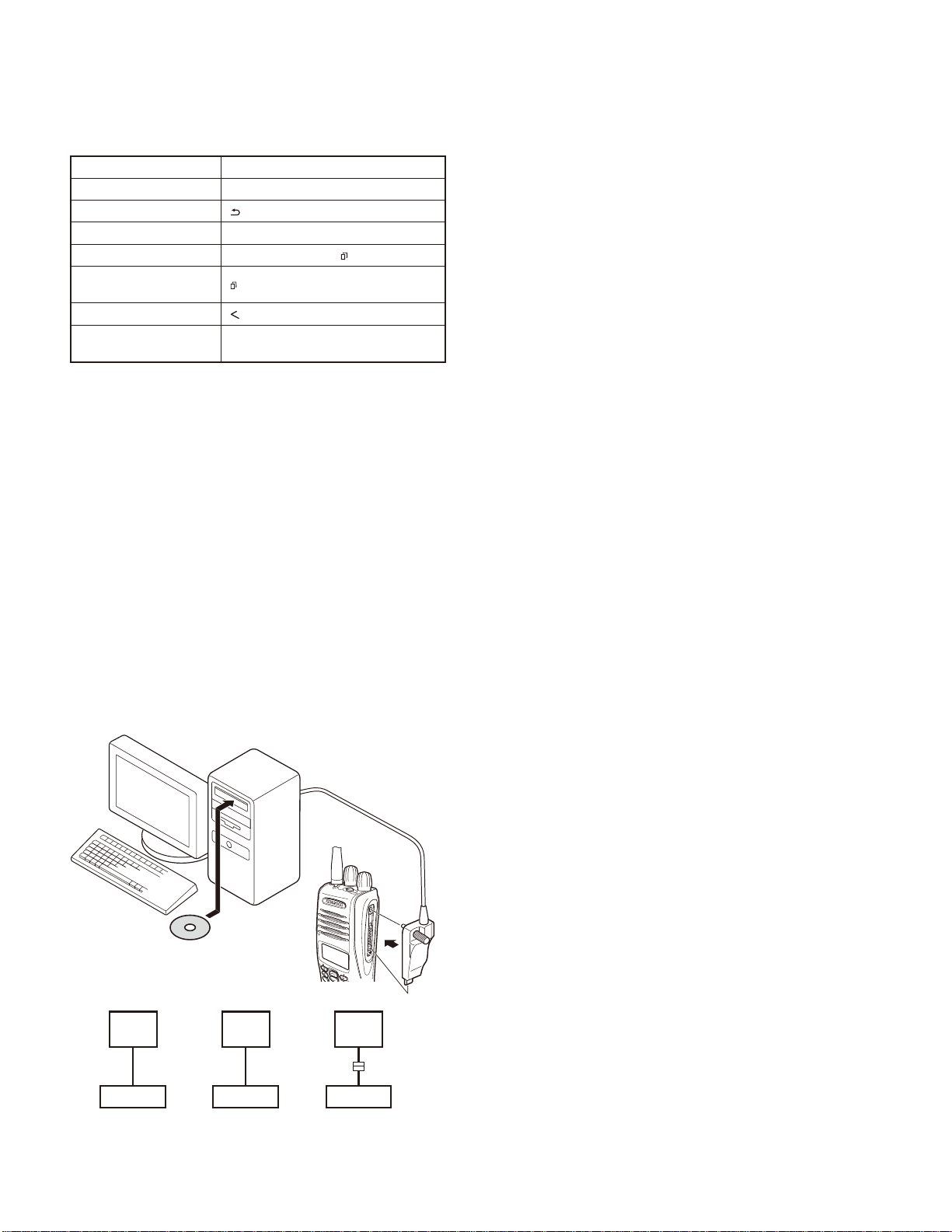
6-2. Connection procedure
Connect the transceiver to the personal computer using
the interface cable (KPG-36A/36U) and USB adapter (KCT-
53U: when the interface cable is KPG-36A, the KCT-53U can
be used.). (Connection is the same as in the PC Mode.)
6-3. Programming
1. Start up the firmware programming software (Fpro.exe
(ver. 6.10 or later)). The Fpro.exe exists in the KPG-111D
installed folder.
2. Set the communications speed (normally, 115200 bps)
and communications port in the configuration item.
3. Set the firmware to be updated by File name item.
4. Press and hold the [ ] key while turning the transceiver
power ON. Then, the orange LED on the transceiver
lights and “PROGRAM 115200” is displayed.
5. Check the connection between the transceiver and the
personal computer, and make sure that the transceiver is
in the Program mode.
6. Press “write” button in the window. When the transceiver
starts to receive data, the [LOADING] display lights.
7. If writing ends successfully, the checksum is calculated
and a result is displayed.
8. If you want to continue programming other transceivers,
repeat steps 4 to 7.
Note:
This mode cannot be entered if the Firmware Program-
ming mode is set to Disable in the Programming soft-
ware.
6-4. Function
1. If you press the [Side2] key while “PROGRAM 115200”
is displayed, the display changes to “PROGRAM 19200”
(The LED blinks green) to indicate that the write speed
is low speed (19200 bps). If you press the [Side2] key
again while “PROGRAM 19200” is displayed, the display
changes to “PROGRAM 38400” (The LED lights red
and orange alternatively). If you press the [Side2] key
again while “PROGRAM 38400” is displayed, the display
changes to “PROGRAM 57600” (The LED blinks orange).
If you press the [Side2] key again while “PROGRAM
57600” is displayed, the display returns to “PROGRAM
115200” (The LED lights orange).
2. If you press the [Side1] key while “PROGRAM 115200”
is displayed, the checksum is calculated, and a result is
displayed. If you press the [Side1] key again while the
checksum is displayed, “PROGRAM 115200” is redis-
played.
Note:
Normally, write in the high-speed mode.
7. Clone Mode
Programming data can be transferred from one transceiv-
er to another by connecting them via their external universal
connectors. The operation is as follows (the transmit trans-
ceiver is the source and the receive transceiver is a target).
The following data cannot be cloned.
• Tuning data
• Embedded message with password
• Model name data
• ESN (Electronic Serial Number) data
Note:
The following data can be cloned.
• Fleet (own)/ID (own) for FleetSync
• Unit ID (own) for NXDN
Key guide on the Read authorization password input screen.
• CONFRM ([ ] key):The password confirmation
• DELETE ([ ] key): Delete the least digit from the current
password number (Press and hold to delete all password
numbers)
• SELECT ([ ] key): Determine the least digit of the pass-
word number
1. Press and hold the [ ] key while turning the transceiver
power ON. If the Read authorization password is set to
the transceiver, the transceiver displays “CLONE LOCK”.
If the password is not set, the transceiver displays “CLONE
MODE”.
2. When you enter the correct password, and “CLONE
MODE” is displayed, the transceiver can be used as the
cloning source. The following describes how to enter the
password.
3.
• How to enter the password using the keypad;
If one of keys 0 to 9 is pressed while the “CLONE LOCK”
is displayed, the pressed number is displayed on the
LCD.
Each press of the key shifts the display in order to the
left.
When you enter the password and press the [ ] or [ ]
key, “CLONE MODE” is displayed if the entered password
is correct. If the password is incorrect, “CLONE LOCK” is
redisplayed.
• How to enter the password using the [ ] and [ ]
keys;
If the [ ] / [ ] key is pressed while “CLONE LOCK” is
displayed, the Read authorization password input screen
is displayed.
If the [ ] key or [ ] key is pressed while the Read
authorization password input screen is displayed, the
number (0 to 9) blinks on the LCD. When you press the
[] key, the currently selected number is determined. If
you press the [ ] key after entering the password in this
procedure, “CLONE MODE” is displayed if the entered
password is correct. If the password is incorrect, “CLONE
LOCK” is redisplayed.
4. Power ON the target transceiver.
REALIGNMENT

NX-411
6
5. Connect the cloning cable (part No. E30-3325-05) to the
universal connectors on the source and target.
6. Press the [ ] key on the source while the source displays
“CLONE MODE”. The data of the source is sent to the
target. While the target is receiving the data, “PROGRAM”
is displayed. When cloning of data is completed, the
source displays “END”, and the target automatically oper-
ates in the User mode. The target can then be operated
by the same program as the source.
7. The other target can be continuously cloned. When the
[] key on the source is pressed while the source displays
“END”, the source displays “CLONE MODE”. Carry out
the operation in step 4 to 6.
Note:
• Cannot be cloned if the password (overwrite password) is
programmed to the target.
• “Model Name” must be same to clone the transceiver.
REALIGNMENT
Cloning cable
(E30-3325-05)
MIC
MIC
Fig. 2
8. FirmwareVersion Information
Press and hold the [Side1] key while turning the trans-
ceiver power ON and then keep pressing and holding the
[Side1] key, the firmware version information appears on the
LCD.
INSTALLATION
Voice Guide & Storage Unit (VGS-1: Option)
■Installing theVGS-1 (Voice Guide & Storage
Unit) in the transceiver
1. Remove the two screws from the cover.
2. Remove the cover by inserting the tip of a pair of twee-
zers into the screw hole of the cover and prying it open.
Note:
Take care that the tip of tweezers is not inserted into the
screw hole of the chassis.
The tip of tweezers must come in contact with the surface
of the chassis.
3. Remove the OPTION PCB from the connector (CN321)
of the TX-RX PCB.
CN321
OPTION PCB

NX-411
7
INSTALLATION
4. Attach the cushion (G13-1974-04) to the VGS-1 as
shown in the figure.
Note:
Be sure to not cover the VGS-1 connector with the cush-
ion.
5. Insert the VGS-1 connector into the connector (CN321)
of the TX-RX PCB.
Cushion
(G13-1974-04)
21x21x1.0mm
VGS-1
VGS-1
CN321
6. Insert the flat spring (G02-1853-03) between the VGS-1
and the chassis as shown in the figure.
7. Attach the cushion (G13-1995-04) on theVGS-1 so that it
is attached to a part (shaded region) of the flat spring.
Note:
Be sure not to cover the spring part of the flat spring with
the cushion.
Spring part
Be sure not to cover the spring part
of the flat spring with the cushion.
VGS-1
Cushion
(G13-1995-04)
20x30x1.0mm
Flat spring
(G02-1853-03)
8. Reinstall the cover using the two screws removed in step
1.

NX-411
8
1. Precautions forWaterproof
• The orange packing material on the reverse side of the
transceiver is important with respect to the waterproof ef-
ficiency of the transceiver. Do not place stickers or other
materials on or around the packing material shown in the
figure, or on the reverse side of the battery pack. Doing
so will impair the waterproof efficiency of the transceiver
and may cause it to break down. Additionally, in order to
prevent damage to the packing material, do not allow it to
come in contact with foreign materials.
2. Precautions for Disassembly
■Removing theTX-RX unit from the chassis
1. Remove the Cord ASSY from the connector (CN301) of
the TX-RX unit a.
2. Remove the Speaker lead wire from the connector (CN5)
of the TX-RX unit b.
3. Remove the VOL/CH FPC from the connector (CN201) of
the TX-RX unit c.
4. Remove the Universal connector FPC from the connector
(CN4) of the TX-RX unit d.
5. Remove the PTT FPC from the connector (CN6) of the
TX-RX unit e.
6. Remove the 14 screws f.
7. Anchor the screw hole of the TX-RX unit using the tip of a
pair of tweezers as shown in the figure. Then, lift the TX-
RX unit to remove it from the chassis g.
Cord ASSY
CN201
CN6
VOL/CH FPC
Universal
Connector FPC
CN5
CN301
CN4
PTT FPC
TX-RX unit
b
ac
d
e
DISASSEMBLY FOR REPAIR
f
f
f
f
f
f
f
g
■Removing theTOP packing (G53-1600-12)
1. Pull the TOP packing to the left to remove the packing
that is fit into the left groove of the chassis a.
2. Pull the TOP packing to the right to remove the packing
that is fit into the right groove of the chassis b.
3. Turn back theTOP packing as shown in the figure c.
4. Remove theTOP packing d.
a
b
c
d
3. Precautions for Reassembly
■Mounting the Display unit onto the chassis
Insert the tab of the speaker holder into the hole in the
upper part of the chassis.
Speaker holder

NX-411
9
DISASSEMBLY FOR REPAIR
■Inserting the rubber spacer (J30-1279-04) onto
the rear panel
1. Bend the two convex parts of the rubber spacer inward a,
then fit the sheet into the space b.
Next, bend the one convex part of the rubber spacer in-
ward c, and insert the sheet into the rubber spacer.
2. Press the rubber spacer, using your fingers, to insert it
between the rubber spacer and the rear panel without
crevice.
Apply the bond (W05-0019-00) or “THREE BOND 1401B”
around the inside of the circle nut before tightening the
circle nut.
Circle nut
Rubber spacer (J30-1279-04)
Sheet (G11-4493-04)
■Mounting the chassis onto the case
1. Place the key top on the chassis. Then, fit the chassis
tightly into the groove of the key top a.
Note:
Confirm that the entire groove of the key top fits to the
chassis tightly.
2. Press the microphone part of the key top using your fin-
ger b.
Note:
Confirm that the microphone part of the key top fits tightly
with the element microphone.
3. Mount the chassis onto the case c.
Note:
After mounting the chassis onto the case, if the 18-key
part on the key top or the Auxiliary (Orange) key part of
the VOL/CH packing gets stuck inside the case as shown
in the figure, return it to the normal position using a soft
tipped item (e.g., your finger) d.
Prying it with a pointed metal tool such as forceps, may
damage the key top or packing.
c
18-key part
Auxiliary
(Orange) key
b
a
d
■Removing the lithium cell (W09-0971-05)
Insert a non-conductive screwdriver to groove of one side
of the socket (CN204) and pry the lithium cell up from the
socket.
■Installing the lithium cell (W09-0971-05)
Insert a lithium cell into one side of the socket (CN204).
Push the lithium cell to insert the lithium cell into the
socket.

NX-411
10
DISASSEMBLY FOR REPAIR
■Forming the Cord ASSY
Form the Cord ASSY according to the procedure shown
in the figure.
TX-RX
J87-0005 S
CONT
TX-RX
J87-0005 S
CONT
CONT
Fold it so that the end of the “TX-RX”
side fit the “
-
” silk screen line.
Turn over the cord ASSY.
Fold it so that the bent part of “TX-RX”
side fit the connector outline of "CONT"
side.
Turn over the cord ASSY.
Fold it so that the bent part of “CONT”
side fits the end of “TX-RX”side.
Cord ASSY is rotated by 180 degrees.
Cord ASSY
Cord ASSY
CN301
TX-RX
unit
■Correspondence when replacing the case
(A02-4076-11)
Apply the dry-surf (410-0019-05) around the LCD and
18-key part of the case when replacing the case.

NX-411
11
DISASSEMBLY FOR REPAIR
■Assembly information (Sheet/Cushion)
When “Main Parts” is changed (ordered), “Assembled Sheet/Cushion” should also be changed (ordered) together.
The Sticker and Sheet etc are non-reusable parts. It requires the new one to get the radio’s performance after repairs.
For example, when “Main Cabinet (A02-4076-11)” is changed, “Sticker (B42-7296-04)”, “Badge (B43-1606-04)” and “Fibrous
Sheet (G10-1400-04)” should be ordered and changed together because Sticker (B42-7296-04), Badge (B43-1606-04) and
Fibrous Sheet (G10-1400-04) are non-reusable.
Main Parts Assembled Sheet/ Cushion
Part Name Part Number Part Name Part Number Remark
Main Cabinet A02-4076-11
Sticker B42-7296-04 “NEXEDGE” is printed.
Badge B43-1606-04 “KENWOOD” is printed.
Fibrous Sheet (SP) G10-1400-04
LCD ASSY B38-0923-05 Adhesive Sheet (LCD) J99-0714-04
Used for fixing the LCD ASSY on the Illumination Guide
(LCD).
Also used for fixing the Illumination Guide (LCD) on the
Control Unit.
Speaker T07-0749-25 Rubber Cushion (SP) G11-4272-14
Chassis A10-4132-03 Rubber Sheet (FET) G11-4308-24 Used for stabilizing the radiation performance of the FET.
Illumination Guide (LCD) B11-1854-02 Sheet (LCD-Holder) G11-4495-14
Packing (18-key) G53-1823-11 Sheet (18-key Pack-
ing) G11-4494-04

NX-411
12
CIRCUIT DESCRIPTION
1. Overview
The NX-411 is an 900MHz Portable transceiver designed
to operate in the frequency range of 896 to 941MHz.
The unit consists of receiver, transmitter, phase-locked
loop (PLL) frequency synthesizer, baseband parts, power
supply, and control circuits.
2. Frequency Configuration
The receiver is a double-conversion superheterodyne us-
ing the first intermediate frequency (IF) of 58.05MHz and the
second IF of 450kHz. Incoming signals from the antenna are
mixed with the local signal from the PLL circuit to produce
the first IF of 58.05MHz.This is then mixed with the 57.6MHz
second local oscillator output to produce the 450kHz second
IF. The transmit signal frequency is generated by the PLL
VCO, and modulated by the signal from the DSP. It is then
amplified and fed to the antenna.
Fig. 2 RF and IF circuit
3. Receiver System
3-1. RF Circuit
An incoming RF signal from the antenna terminal is
passed through the antenna switch (D605, D606, D607 and
D608) and then the band-pass filter (L830).
The signal is amplified by an RF amplifier (Q804), and
passed through the band-pass filter (L820). The resulting
signal is applied to the first mixer (IC804), where it is mixed
with the first local oscillator signal output from the frequency
synthesizer to produce the first IF (58.05MHz).
3-2. IF Circuit
The first IF signal is passed through a four-pole mono-
lithic crystal filter (XF801) to reject adjacent channel signals.
The filtered first IF signal is amplified by the first IF amplifier
(Q802) and then applied to the lF system IC (IC802). The
IF system IC provides a second mixer, AGC amplifier, and
RSSI (Received Signal Strength Indicator).
The second mixer mixes the first IF signal with the
57.6MHz of the second local oscillator output and produces
the second IF signal of 450kHz.
The second IF signal is passed through the ceramic filter
(CF801) to reject the adjacent channel signal. The filtered
second IF signal is amplified by the AGC amplifier.
The signal from the AGC amplifier is input to the ASIC
(IC309) through the ceramic filter (CF802) and operational
amplifier (IC801).
x3
ANT
SW LNA 2nd Mixer
IF AMP
PLL
VCO
ANT
58.05MHz
19.2MHz
993.05~
999.05MHz
896~902MHz (TX)
935~941MHz (RX/TX)
896~902MHz
935~941MHz
MCF
TCXO
ASIC
A/D
D/A
DSP
CF
450kHz
AF
AMP
PA
AMP TX
AMP MIC
AMP
TX/RX
SW
1st Mixer SP
MIC
Fig. 1 Frequency configuration
ANT
SW LNABPF FM IC
D605, D606
D607, D608 L830
BPF
L820
BPF
CF802
AMP
IC801
ASIC
IC309
BPF
XF801
TCXO
X501
BPF
CF801
IF
AMP
Q802
AMP
(x3)
Q801
IC802
1st
Mixer
IC804
1st Lo
Q804

NX-411
13
CIRCUIT DESCRIPTION
3-3. Audio Amplifier Circuit
Audio processing (high-pass filter, low-pass filter, de-
emphasis, etc.) at FM mode and decoding at NXDN mode
are processed by the DSP.The audio signal from IC309 and
IC304 goes through the amplifier (IC2).The signal then goes
through a mute switch (IC7), amplifier (IC10), electronic vol-
ume control (IC3), and AF amplifier (IC13).
While busy, AMT becomes Low to turn on IC2, and the
signal is fed to the AF switch. While INAMT is High, the AF
switch (IC15) selects the internal speaker, and the audio
signal is fed to the internal audio power amplifier (IC17),
AMPASIC
DSP
SP
Drive AMP
IC309
IC304
SW
IC7
AMT
VOL
IC3 IC13
AMP
IC10IC2
IC15
Q7
Q11
Shut down
Shut down
Vdd
IC17
IC19
INAMT
B
EXAMT
INT. SP
EXT. SP
and is then output to the internal speaker. While EXAMT is
High, the AF switch (IC15) selects the external speaker, and
the audio signal is fed to the external audio power amplifier
(IC19), and is then output to the external speaker.The power
supply for IC17 and IC19 is turned on while INAMT or EX-
AMT is High.
The speaker is switched by the logic of the speaker
switching terminal SSW on the universal connector. When
the SP-MIC is not attached, SSW becomes High. IC309
detects the logic of SSW and activates either INAMT or EX-
AMT.
Fig. 3 Audio amplifier circuit
3-4. Squelch Circuit
It amplifies the demodulated noise signal from IC309
after filtering through the BPF circuit. The amplified signal is
then converted to a DC signal by the detection circuit. The
converted signal is fed back to IC309.
LPFDET
IC309
HPF
IC16
RECT
D7
AMP
IC16
AMP
Q12IC11
Fig. 4 Squelch circuit

NX-411
14
CIRCUIT DESCRIPTION
4.Transmitter System
4-1. Audio Band Circuit
The signal from the internal microphone goes through
the mute switch (Q9). When the SP-MIC is not attached, the
microphone switching terminal (MSW) on the universal con-
nector becomes High, and the mute switch (Q9) is turned
on. When the SP-MIC is attached, MSW is connected to
GND inside of the SP-MIC. For this reason, Q8 is turned off,
the internal microphone is muted, and only the input of the
external microphone is supplied to the microphone ampli-
fier. The signal from the microphone goes through the mute
switch (Q6), and is amplified by IC14 and limited by the AGC
circuit which is composed of D1, D2, Q3 and Q4.
SW
Q9
Q8
MSW
INT. MIC
EXT. MIC
LPF
IC1
AMP
IC5
DAC
IC3
AMP
IC505
VCO
SW
MM
Q6
SW
SCSW
IC8
AMP
AGC
Q3, Q4
D1, D2
IC14
AMP
IC5
TCXO
X501
LPF
IC4
PLL
IC503
ASIC
IC309
DSP
IC304
4-2. Baseband Circuit
The audio signal from the audio band circuit is converted
to digital data with a sampling frequency of 48kHz with ASIC
(IC309). This digital data is sent to the DSP (IC304), and
voice signals of 300Hz or lower and frequencies of 3kHz or
higher are cut off and an audio range of 300Hz to 3kHz is
extracted.
In FM mode, the audio signal is pre-emphasized and
combined with signals, such as QT and DQT, as required.
In Digital mode, the audio signal is converted to the
4-Level FSK baseband signal. The baseband signals of
DTMF and MSK are also generated by the DSP.
The processed baseband signal is output from IC304
and IC309. The signal from IC304 deviates the frequency of
the PLL IC (IC503).The signal from IC309 is filtered with the
LPF (IC1), and adjusts the level with DAC (IC3), and devi-
ates the frequency of the VCO.
Fig. 5 Audio band and Baseband circuit

NX-411
15
CIRCUIT DESCRIPTION
4-3.VOX
IC14 amplifies the audio signal captured in the micro-
phone. The signal is then converted into DC voltage, and is
rectified by D3. The DC voltage activates the ASIC (IC309),
and the VOX starts.
4-4. Drive and Final Amplifier
The signal from the T/R switch (D601 is on) is amplified
by the drive amplifier (Q610, Q601 and Q602) to 23~26dBm.
The output of the drive amplifier is amplified by the RF
power amplifier (Q604) to 2.5W (1W when the power is low).
The RF power amplifier is a MOS FET. The output of the RF
power amplifier is then passed through the harmonic filter
(LPF) and antenna switch (D605 and D606 are on) and ap-
plied to the antenna terminal.
TX/RX
SW
D513, D601
+B R650
R651
VDD
VGG
REF Vol
(IC505)
AMP
Q610 Drive
AMP
Q602
Pre-Drive
AMP
Q601 Final
AMP
Q604
IC601
(2/2)
IC601
(1/2)
ANT
SW
D605, D606
D607, D608
LPF
ANT
4-5. APC Circuit
The APC circuit always monitors the current flowing
through the RF power amplifiers (Q604 and Q602) and
keeps a constant current. The voltage drop at R650 and
R651 is caused by the current flowing through the RF power
amplifiers. This voltage is applied to the differential amplifier
(IC601 1/2).
IC601 (2/2) compares the output voltage of IC601 (1/2)
with the reference voltage from IC505, and the output of
IC601 (2/2) controls the VGG of Q601, Q602 and Q604 to
make both voltages the same.The change of power high/low
is carried out by the change of the reference voltage. Q606,
Q608 and Q609 are turned on and Q605 is turned off during
transmission and the APC circuit is active.
Fig. 6 Drive and final amplifier and APC circuit
5. PLL Frequency Synthesizer
5-1.TCXO (X501)
TCXO (X501) generates a reference frequency of
19.2MHz for the PLL frequency synthesizer. This reference
frequency is applied to pin 9 of the PLL IC (IC503) and is
connected to the IF circuit as a 2nd local signal through the
Tripler (Q801). The oscillation frequency of TCXO is deter-
mined by the DC voltage of the VC terminal.The VC voltage
is fixed to 1.65V by R501 and R502.
The frequency adjustment is achieved by switching the
ratio of dividing frequency that is not adjusted by the DC
voltage impressed toVC.
5-2.VCO
There are two VCOs (RX VCO and TX VCO).
RX VCO (Q507) generates the 1st local signal for the re-
ceiver.
TX VCO (Q504) generates a carrier for the transmitter
and a carrier for the transmitter ofTA (Talk Around).
The oscillation frequency of the VCO is half of the carrier
or 1st local signal.The VCO oscillates from 448 to 470.5MHz
during transmit, and from 496.525 to 499.525MHz during
reception.
The VCO oscillation frequency is determined by one sys-
tem of operation switching terminal “/T_R” and two systems
of voltage control terminals “CV” and “ASSIST”.
The operation switching terminal, “/T_R”, is controlled by
the control line (/T_R) output from the ASIC (IC309). When
the /T_R logic is low, TX VCO is activated, and when the /T_
R logic is high, RX VCO is activated.
The voltage control terminals, “CV” and “ASSIST”, are
controlled by the PLL IC (IC503) and ASIC (IC309) and the
output frequency changes continuously according to the
applied voltage. For the modulation input terminal, “VCO_
MOD”, the output frequency changes according to the ap-
plied voltage.This is used to modulate the VCO output.

NX-411
16
CIRCUIT DESCRIPTION
5-3. PLL IC (IC503)
The PLL IC compares the differences in phases of the
VCO oscillation frequency and the TCXO reference fre-
quency, returns the difference to the VCO CV terminal and
realizes the “Phase Locked Loop” for the return control. This
allows the VCO oscillation frequency to accurately match
(lock) the desired frequency.
When the frequency is controlled by the PLL, the fre-
quency convergence time increases as the frequency differ-
ence increases when the set frequency is changed. To sup-
plement this, the ASIC is used before control by the PLL IC
to bring the VCO oscillation frequency close to the desired
frequency. As a result, the VCO CV voltage does not change
and is always stable at approximately 2.8V at the time of re-
ceive mode. At the time of transmitit mode, it is always stable
at approximately 3.0V.
The desired frequency is set for the PLL IC by the ASIC
(IC309) through the 3-line “SDO1”, “SCK1”, “/PCS_RF” se-
rial bus.Whether the PLL IC is locked or not is monitored by
the ASIC through the “PLD” signal line. If the VCO is not the
desired frequency (unlock), the “PLD” logic is low.
“PLLMOD” receives the modulation data from the DSP
(IC304).
5-4. Doubler (Q509)
The doubler (Q509) extracts the twice harmonic com-
ponent from the signal from the VCO. This twice harmonic
components is fed into the PLL (IC503) and buffer (Q510)
through a band-pass filter.
5-5. Local Switch (D513, D601)
The destination of the signal from the buffer amplifier
(Q510) is changed with the diode switch (D601) that is con-
trolled by the transmission power supply, 50T, and the diode
switch (D513) that is controlled by the receive power supply,
50R. If the 50T logic is high, it is connected to a send-side
pre-drive (Q610). If the 50T logic is low, it is connected to a
receive-side mixer (IC804).
Fig. 7 PLL block diagram
Ripple
filter
Q503 Q505
Q506
5C
/T_R
Ripple
filter
PLL IC
TCXO
IC503
X501
DAC
Q504, Q507
RX VCO
TX VCO
Q501
ASIC
SD1, SCK1, PLD
CV
PLL MOD
IC309
DSP
IC304
TX/RX
SW
D513, D601
IC3
IC504
Q502
BUF
Q508
BUFBUF
IC505
VCO_MOD
BUF
Q510
BUF
Q509
x2

NX-411
17
CIRCUIT DESCRIPTION
6. Control Circuit
The control circuit consists of the ASIC (IC309) and its
peripheral circuits.IC309 mainly performs the following;
1) Switching between transmission and reception by PTT
signal input.
2) Reading system, zone, frequency, and program data from
the memory circuit.
3) Sending frequency program data to the PLL.
4) Controlling squelch on/off by the DC voltage from the
squelch circuit.
5) Controlling the audio mute circuit by decode data input.
6-1. ASIC
The ASIC (IC309) is a 32-bit RISC processor, equipped
with peripheral function and ADC/DAC.
This ASIC operates at 18.432MHz clock and 3.3V/1.5V
DC. It controls the flash memory, SRAM, DSP, receiver cir-
cuit, transmitter circuit, control circuit, and display circuit and
transfers data to or from an external device.
6-2. Memory Circuit
The memory circuit consists of the ASIC (IC309), the
SRAM (IC305), and the flash memory (IC303).
The flash memory has a capacity of 32M-bit that contains
the transceiver control program for the ASIC and stores the
data. It also stores the data for transceiver channels and op-
erating parameters that are written by the FPU.This program
can be easily written from external devices. The SRAM has
a capacity of 1M-bit that contains work area and data area.
■Flash memory
Note: The flash memory stores the data that is written by
the FPU (KPG-111D), tuning data (Deviation, Squelch, etc.),
and firmware program (User mode,Test mode, Tuning mode,
etc.). This data must be rewritten when replacing the flash
memory.
■SRAM (Static memory)
Note: The SRAM has a temporary data area and work area.
When the power supply is off, it is backed up by an internal
secondary lithium battery. Therefore, the saved data is not
lost.
■Real-time clock
The clock function is based on a real-time clock IC (IC308).
When the power supply is off, it is backed up by an internal
secondary lithium battery.
6-3. LCD
The LCD is controlled using the bus lines on the con-
nector (CN301) of the Display unit (X54-377). It corrects the
LCD contrast voltage using IC102.
6-4.Temperature Detection Circuit
The temperature detection circuit detects the temperature
using a temperature IC (IC502) and corrects the thermal
characteristic change of the squelch or LCD.
6-5. Key Detection Circuit
Keys are detected using a key scan circuit in IC309. The
/KEYI*signals that are normally pulled down go high when
any key is pressed.
6-6. Low BatteryWarning
The battery voltage is divided using R224 and R225 and
is detected by the ASIC (IC309). When the battery voltage
falls below the voltage set by the Low battery warning ad-
justment, the red LED blinks to notify the operator that it is
time to replace the battery. If the battery voltage falls even
more (approx. 5.8V), a beep sounds and transmission stops.
Low battery warning Battery condition
The red LED blinks during
transmission. The battery voltage is low but
the transceiver is still usable.
The red LED blinks and the
warning tone beeps while the
PTT switch is pressed.
The battery voltage is low and
the transceiver is not usable to
make calls.
6-7. DSP
The DSP circuit consists of a DSP (IC304) and process-
es the baseband signal. The DSP operates on an external
clock of 18.432MHz (the same as IC309), the I/O section
operates at 3.3V and the core section operates at 1.5V. The
DSP carries out the following processes:
• 4 Level FSK processing
• Analog FM pre-emphasis/de-emphasis
• Vocoder processing between audio codec and modula-
tion/demodulation
• CAI processing, such as error correction encoding
• QT/DQT encoding/decoding
• LTR encoding/decoding
• DTMF encoding/decoding
• MSK encoding/decoding
• Compressor/expander processing
• Voice scrambler processing
• Transmit/receive audio filtering processing
• Microphone amplifier AGC processing
• Audio mute processing
• Modulation level processing
7. Power Supply Circuit
The battery voltage (+B) is provided from the battery ter-
minal on the TX-RX unit (X57). The battery voltage passes
through the 2.5A fuse (F201), and goes to the RF final am-
plifier, AVR ICs (IC204, IC205, IC210, IC18), DC/DC (IC206)
and voltage detector IC (IC209).
The voltage detector watches the battery voltage. If the
battery voltage is 5.6V or higher, the detector outputs High.
While the output of IC209 is High, IC210 and Q208 provide
3.1V (31BU) to the backup-section.
When the VOL SW is turned on, SB1 becomes high (bat-
tery voltage). The DC/DC (IC206) operates if both SB1 and
the output of the detector are high. IC206 outputs 3.8V and
activates IC203 (33M), IC202 (15M), and IC201 (33A). As a
result, the ASIC and DSP operate.

NX-411
18
The SBC signal becomes High after the ASIC operates,
and IC204 (5A) and Q201 (SB2) are turned on. IC207 oper-
ates by turning on these AVR ICs and FET switches.
The 5UC signal becomes High when an option is in-
stalled on the universal connector. Then IC18 (50U) oper-
ates.
When the /SAVE signal becomes High, IC205 (50C) op-
erates.The output of IC205 is connected to two FET switch-
es (Q207, Q205). When the SBC signal becomes High,
IC207 (33C) operates. The FET switches are controlled by
the ASIC. Q207 (50T) is turned on in transmit mode. Q205
(50R) is turned on in receive mode.
When the VOL SW is turned off, the /PSW signal be-
comes Low. After detecting the /PSW signal, the ASIC
changes the SBC signal to Low. Then the power supplies
except IC210 (31BU) stop.
IC205
AVR IC
IC309
ASIC
+B
50C
50T
50R
SB2
5A
–10V
50U
31BU
33C
33M
15M
33A
RX circuit
Option
LCD bias
Universal
SRAM, RTC
PLL, VCO
ASIC, DSP I/O,
FLASH, LCD DRV
RF Final AMP
APC
/SAVE
/5TC
/5RC
5UC
SBC
VCO
TX circuit
Backlight,
Key Light,
TX/Busy LED
ASIC, DSP core
ASIC Analog,
Audio
/PSW
/BINT
F201
Q207
50T SW
IC105
DC/DC
Q205
50R SW
Q208
31BU
Q203
Lvl Conv
Q206
AND D213
OR
VoL SW
SBC
SB1
Q201
SB2 SW
IC210
AVR IC
IC18
AVR IC
IC207
AVR IC
IC206
DC/DC
IC209
Detect
IC203
AVR IC
IC202
DC/DC
IC201
AVR IC
Q204
Lvl Conv
D212
OR
IC204
AVR IC
Fig. 8 Power supply circuit
8. Signaling Circuit
8-1. Encode (QT/DQT/LTR/DTMF/MSK)
Each signaling data signal of QT, DQT, LTR, DTMF and
MSK is generated by the DSP circuit, superimposed on a
modulation signal and output from the DSP (IC304) and
ASIC (IC309). The modulation balance of the QT/DQT/LTR
signal is adjusted by the D/A converter (IC3) and the result-
ing signal is routed to the modulation input of the VCO and
PLL IC (IC503). Each deviation of the TX QT, DQT, LTR,
DTMF and MSK tone is adjusted by changing the output lev-
el of IC304 and the resulting signal is routed to the VCO and
PLL IC (IC503). The RX DTMF tone is routed to the receive
audio signal system, and is output from the speaker.
8-2. Decode (QT/DQT/LTR/DTMF/MSK)
The audio signal is removed from the FM detection signal
sent to the DSP circuit and the resulting signal is decoded.
9. Compander Circuit
The term “compander” means compressor and expander.
The compander reduces noise by utilizing a compressor
and an expander.The transceiver contains a DSP (IC304) to
perform this operation. The transceiver compander can be
turned on or off using the FPU.
CIRCUIT DESCRIPTION

NX-411
19
Display unit (X54-3770-10)
Ref. No. Part Name Description
IC102 IC LCD contrast
IC105 IC Voltage doubling inverter
D1~4 LED 6key backlight
D5~10 LED 12key backlight
D11~14 Diode 12key control
D15~18 LED LCD backlight
COMPONENTS DESCRIPTION
TX-RX unit (X57-8120-10)
Ref. No. Part Name Description
IC1,2 IC OP AMP (AF)
IC3 IC DA converter
IC4 IC OP AMP (MIC)
IC5 IC OP AMP (AF)
IC6,7 IC Logic switch (AF)
IC8 IC Logic switch (MIC)
IC9 IC Logic switch (AF)
IC10 IC OP AMP (AF)
IC11 IC OP AMP (RF control)
IC12~14 IC OP AMP (AF)
IC15 IC Logic switch (AF)
IC16 IC OP AMP (AF)
IC17 IC SP AMP
IC18 IC AVR (50U)
IC19 IC SP AMP
IC20 IC Logic AND
IC21,22 IC Voltage level conversion
IC201 IC AVR (33A)
IC202 IC DC/DC converter (15M)
IC203 IC AVR (33M)
IC204 IC AVR (5A)
IC205 IC AVR (50C)
IC206 IC DC/DC converter (3.8V)
IC207 IC AVR (33C)
IC208 IC OP AMP (50T)
IC209 IC Voltage detector
IC210 IC AVR (Backup)
Ref. No. Part Name Description
IC301,302 IC Bus switch (LCD)
IC303 IC Flash memory
IC304 IC DSP
IC305 IC SRAM
IC306 IC Reset
IC307 IC Logic AND
IC308 IC RTC
IC309 IC ASIC
IC310 IC Buffer AMP (18.432MHz)
IC311 IC I/O expander
IC312 IC Logic AND
IC502 IC Temperature detection
IC503 IC PLL IC
IC504 IC OP AMP (PLL)
IC505 IC OP AMP (RF control)
IC601 IC APC AMP
IC801 IC Buffer AMP (RX)
IC802 IC IF IC
IC803 IC OP AMP (RF control)
IC804 IC Mixer (RX)
Q1 FET DC switch
Q3,4 Transistor MIC AGC
Q5 FET DC switch
Q6 FET DC switch (MIC)
Q7,8 FET DC switch
Q9 FET DC switch (MIC)
Q10,11 Transistor DC switch
Q12 Transistor Noise AMP
Q13 FET DC switch
Q201~205 FET DC switch
Q206~208 Transistor DC switch
Q209,210 FET DC switch
Q211~214 Transistor DC switch
Q301~303 Transistor DC switch
Q304 FET DC switch
Q305 Transistor DC switch
Q306 FET DC switch
Q501 Transistor DC switch
Q502 FET Buffer AMP (CV)
Q503 Transistor DC switch
Q504 FET VCO
Q505 FET DC switch
Q506 FET DC switch (VCO)
Q507 FET VCO
Q508~510 Transistor Buffer AMP (VCO)

NX-411
20
COMPONENTS DESCRIPTION
Ref. No. Part Name Description
Q601 FET Buffer AMP (TX)
Q602 FET Drive AMP
Q604 FET Final AMP
Q605 FET DC switch
Q606,607 Transistor DC switch
Q608 FET DC switch
Q609 Transistor DC switch
Q610 Transistor Buffer AMP (TX)
Q801 Transistor Buffer AMP (2nd Local)
Q802 Transistor IF AMP
Q804 FET Buffer AMP (LNA)
D1,2 Diode MIC AGC
D3,4 Diode Speed up diode
D5,6 Diode Reverse current prevention
D7 Diode Squelch rectification
D8~15 Diode Reverse current prevention
D16,17 Zener diode Surge absorption
D18,19 Diode Surge absorption
D20~23 Zener diode Surge absorption
D201,202 Diode Speed up diode
D204 Diode Protect of DC power
D205 Diode Logic OR
D206 Diode Reverse current prevention
D207 Diode DC/DC converter
D208 Diode Reverse current prevention
D209 Diode Speed up diode
D210,211 Diode Reverse current prevention
D212,213 Diode Logic OR
D214 Diode Reverse current prevention
D215 LED TX/RX LED
D301,302 Diode Reverse current prevention
D501,502 Diode Speed up diode
D504 Diode Speed up diode
D505~512 Variable
capacitance
diode VCO (Frequency control)
D513 Diode TX/RX RF switch
D601 Diode TX/RX RF switch
D604 Zener diode Voltage limiting
D605~608 Diode TX/RX RF switch
D801 Diode Protect of RF power
Table of contents
Other Kenwood Transceiver manuals

Kenwood
Kenwood TK-5710(H) User manual

Kenwood
Kenwood NEXEDGE NX-720 User manual

Kenwood
Kenwood TH-26A User manual

Kenwood
Kenwood TK-2400 User manual

Kenwood
Kenwood TM-251A User manual

Kenwood
Kenwood TS-950SDX User manual

Kenwood
Kenwood TH-22A User manual

Kenwood
Kenwood TS-990S User manual

Kenwood
Kenwood TS-780 User manual

Kenwood
Kenwood TH-G71A User manual

Kenwood
Kenwood TK-2302 User manual

Kenwood
Kenwood TK-2140 User manual

Kenwood
Kenwood NX-5200E User manual

Kenwood
Kenwood TK-6110 User manual

Kenwood
Kenwood TK-3170 E3 User manual

Kenwood
Kenwood TK-D200G User manual

Kenwood
Kenwood TK-2317 User manual

Kenwood
Kenwood TK-752 User manual

Kenwood
Kenwood TK-3312 User manual

Kenwood
Kenwood TK-7360 User manual