bw
INTRODUCTION
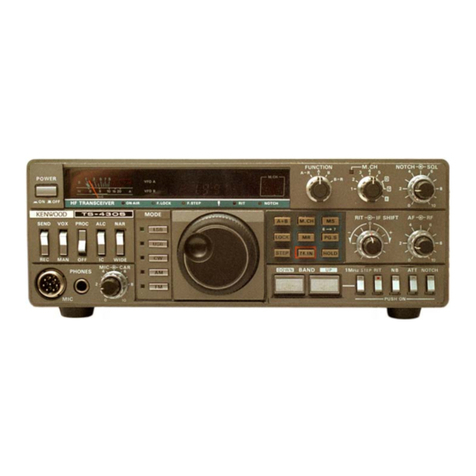
The TS-830s 1s a dual conversion transceiver using two in-
termediate frequencies, 8.83 MHz and 455 kHz. However.
this differs from transceivers of the 'socalled Colllns type(such
as the TS-520) in that the bandwidth of both intermediate
frequencies
IS
narrowed for perforrr~ingVBT operation
Therefore, the TS-830s can basically be considered a single
conversion transcelver wlth an 8.83 MHz IF
Operation of the transmitter is opposite In process to the
receiver AN SSB signal generated at 455 kHz
IS
con-
.-
-.
-
.
-
-. -.
verted to 8.83MHz, and is then m~xedwith the PLL (local0s-
Table 2. Crystalfilter (L71-0222-05)
YK88S1 (IFunit, XFI)
cillator output) to produce the final transrriission frequency
Item
Center frequency lo
Centerfrequency dev~ation
Pass bandw~dth
Attenuation bandwidth
Ripple
Loss
Guaranteed attenuation
(lo
+lOkHzto!o+l MHz)
Inputand output
impedance
The circuitry is hybrid with vacuum tubes used only in the
drlver
(
12BY7A) and flnal-stage power amplifier (6146B's)
The PLL circu~tgeneraies a heterodyne frequency for each
band, a counter reference signal, and a 25 kHz marker, all
Ratlng
8831.5
kHz
W~th~n
r250Hz
at
6
dB
+3
0 kHz
or
more
at
6
dB
f
6kHz
or lessat
60
dB
?
10kHz
or less at
80
dB
2
dB or less
3
dB w~thin
t2
dB
.
80
dB or more
600!1//15PF
from
a
single crystal oscillator
The TS-830s Incorporates an IF SHIFT circuit, VBT, VOX
Table
3.
Crystalfilter (L71-0223-05)
YK-88A (IF unit. XF2)
(also used for CW seml break-in),slde tone circuit, RF speech
processor, -transmiss~onmonitor clrcuit, nolse blanker, XTAL
calibrator, notch filter, and etc.
RECEIVER CIRCUIT
The signal comlng from the antenna is routed through step-
up antenna coil via an RF ATT switch and IF trap. MOS FET
(Q1 3SK73) amplifies this slgnal Approximately 9 dB of
negatlve feedback is applied to -the RF amplifier to reduce
nolse and expand the amplifiers range of linear
operation
The signal passes through a buffer amplifier (Q2 2SK125)
and is m~xedwith the PLL VCO output by a balanced mixer
((23, Q4 2SK125) The signal is now converted to the first
lntermedlate frequency, 8.83 MHz. Entering the IF unit, this
signal is amplif~edby Q1 (2SK125),passes through ceramic
filter CF1 and the NB gatlng circult, and is applled to crystal
filter XF1 whose center frequency is 8.83 MHz. The signal
leaving the crystal filter is mixed wlth the VBT local oscillator
output at 8.375 MHz by a balanced mixer (Q2,03 3SK73)
where it
IS
converted to the second Intermediate frequency,
455
kHz. The signal then passes through ceramic filter CF2
whose center frequency is 455 kHz, and is amplified by 04
(3SK73) It then
IS
fed to the notch circuit, Q5 through Q7
(2SC1815) After being amplified by Q8 (3SK73), it is
demodulated to an audio srgnal by the product detector
(D20--D23, IN60 X4)
In the AF unit, the audio s~gnal is amplified by Q3
(2SC2240), passes through the AF GAIN control and after
belng arnpllf~edby the power amplif~erQ4 (HA1368R).
drives the speaker
Table 4. Ceramic filter (L72-0314-15)
CFJ455K5 (IFunit, CF2)
L
Item
Center frequencyfo
3
dB bandwidth
30
dB
bandwidth
Input level (at
80
dBp output)
Ripple (within3 dB handwidth)
Spurious response
Input and output impedance
TRANSMITTER CIRCUIT
Item
Centerfrequency
6
dB bandwidth
--
60
dB bandw~dth
Rating
8.830
MHz
fo
f
5
kHz
or more. total
25
kHz
or more
100
kHz
or less
93.5dB or less
1
dB or less
20
dB or more
within fo
+
1.5
MHz
330R
Audlo input picked up by the m~crophonecomes to the IF
unit and
IS
amplif~edby Q19-21 The input circuit adapts
to any m~crophoneimpedance of from 500 ohms to 50k
ohms. This ampl~f~edoutput
IS
converted to a DSB signal by
the balanced modulator D29-32
(1N60
X
4),passes through
buffer
amplifier
Q22 (2SK1
9),
a 455kHz ceramic filter, and
the output appears as a SSB slgnal This signal passes either
buffer amplifier Q23 (2SC1815), or the speech processor
consisting
of Q24, 26, and 27 Then the first transmit mixer
(Q28 3SK73) converts thls to an 8.83 MHz SSB signal
After passing the 8.83 MHz crystal filter and being amplified
by Q29 (3SK73),the signal is applied to the second transmit
mixer in the RF unit. This. double balanced mixer (Q6,
Q7 3SK73), mlxes the slgnal with the PLL VCO output to
convert to the final Transmlt frequency Output is amplif~ed
by the driver tube (V1 12BY7A)and then by the final power
amplifier (two 6146B's) and is applied to the antenna via
a
T-matching network.
Guaranteed attenuat~on
6
dB or less
Guaranteed attenuat~on
60
dB or more
(lo
+
100kHz1
impedance
LOSS
6
d~
Table 5. Ceramic filter (L72-0322-05)
Inputand output ~mpedance
2
k!2
CFW456.5HT (IFunit, CF 3)
Item
Centerfrequency lo
6
dB bandw~dth
50
dB bandw~dth
R~pple(io
+2kHz)
Rat~ng
455 kHz
+
0 2 kHz
2
7
kHz
or more
4 5 kHz
or less
PLL
CIRCUIT
The PLL s~gnalis synthesized from the VFO, CAR, and VCO
outputs. The TS-830s .employs a programmable divider in
the PLL to synthesize the heterodyne frequency from the
standard reference oscillator frequency This simplifies the
Rating
456.5 kHz
t
3
kHz
or more
+9
kHz
or less
2
dB or less
PLL circuitry by eliminatin'gthe need for a separate HET
XTAL for each band
---
Table 1. Ceramic filter pair (L72-0310-05)
2
pcs.
SFA8.83MF combined (IF unit, CF1A&
B)


