Lattice Semiconductor OpenLDI/FPD-LINK/LVDS User manual

OpenLDI/FPD-LINK/LVDS Receiver
Interface IP
User Guide
FPGA-IPUG-02021-1.1
April 2019

OpenLDI/FPD-LINK/LVDS Receiver Interface IP
User Guide
© 2017-2019 Lattice Semiconductor Corp. All Lattice trademarks, registered trademarks, patents, and disclaimers are as listed at www.latticesemi.com/legal.
All other brand or product names are trademarks or registered trademarks of their respective holders. The specifications and information herein are subject to change without notice.
2 FPGA-IPUG-02021-1.1
Contents
1. Introduction..................................................................................................................................................................5
1.1. Quick Facts ..........................................................................................................................................................5
1.2. Features...............................................................................................................................................................6
1.3. Conventions.........................................................................................................................................................6
1.3.1. Nomenclature.................................................................................................................................................6
1.3.2. Data Ordering and Data Types .......................................................................................................................6
1.3.3. Signal Names ..................................................................................................................................................6
2. Functional Descriptions ................................................................................................................................................7
2.1. Interface and Timing Diagrams ...........................................................................................................................9
2.2. Clock, Reset and Initialization ...........................................................................................................................17
2.2.1. Reset and Initialization .................................................................................................................................17
2.2.2. Clock Domains and Clock Domain Crossing..................................................................................................17
2.3. Design and Module Description ........................................................................................................................18
2.3.1. FPD-Link Rx Wrapper Module ......................................................................................................................18
2.3.2. FPD-Link Rx Module......................................................................................................................................19
2.3.3. LVDS71 DDR Group Module .........................................................................................................................22
2.3.4. GDDR SYNC Module .....................................................................................................................................23
2.3.5. BW ALIGN Module........................................................................................................................................24
2.3.6. CLKDIV ..........................................................................................................................................................24
2.3.7. ECLKSYNC......................................................................................................................................................24
2.3.8. GPLL..............................................................................................................................................................25
2.3.9. LVDS71 Pixel Map Module ...........................................................................................................................25
2.3.10. Test Mode Module .......................................................................................................................................26
2.3.11. Synchronizer Module....................................................................................................................................28
3. Compiler Directives and Parameter Settings..............................................................................................................29
3.1. Parameters Settings ..........................................................................................................................................29
3.2. Compiler Directives ...........................................................................................................................................30
4. Debug Features...........................................................................................................................................................31
4.1. Test Mode .........................................................................................................................................................31
5. IP Generation and Evaluation .....................................................................................................................................32
5.1. Licensing the IP..................................................................................................................................................32
5.2. Getting Started..................................................................................................................................................32
5.3. Generating IP in Clarity Designer ......................................................................................................................33
5.4. Generated IP Directory Structure and Files.......................................................................................................35
5.5. Running Functional Simulation .........................................................................................................................37
5.6. Simulation Strategies ........................................................................................................................................38
5.7. Simulation Environment....................................................................................................................................38
5.8. Instantiating the IP ............................................................................................................................................39
5.9. Synthesizing and Implementing the IP..............................................................................................................39
5.10. Hardware Evaluation.........................................................................................................................................40
5.10.1. Enabling Hardware Evaluation in Diamond..................................................................................................40
5.11. Updating/Regenerating the IP...........................................................................................................................40
5.11.1. Regenerating an IP in Clarity Designer .........................................................................................................40
References ..........................................................................................................................................................................41
Technical Support Assistance .............................................................................................................................................41
Appendix A. Resource Utilization .......................................................................................................................................42
Appendix B. What is Not Supported...................................................................................................................................43
Revision History ..................................................................................................................................................................44

OpenLDI/FPD-LINK/LVDS Receiver Interface IP
User Guide
© 2017-2019 Lattice Semiconductor Corp. All Lattice trademarks, registered trademarks, patents, and disclaimers are as listed at www.latticesemi.com/legal.
All other brand or product names are trademarks or registered trademarks of their respective holders. The specifications and information herein are subject to change without notice.
FPGA-IPUG-02021-1.1 3
Figures
Figure 1.1. Sample OpenLDI/FPD-LINK/LVDS Receiver interfaced to MIPI DSI System Diagram .........................................5
Figure 2.1. Top Level Block Diagram.....................................................................................................................................7
Figure 2.2. OpenLDI/FPD-LINK/LVDS Input Bus Waveform..................................................................................................9
Figure 2.3. Single Channel OpenLDI/FPD-LINK/LVDS Input Bus Waveform for RGB888 Format........................................10
Figure 2.4. Dual Channel OpenLDI/FPD-LINK/LVDS Input Bus Waveform for RGB888 Format..........................................11
Figure 2.5. Single Channel OpenLDI/FPD-LINK/LVDS Input Bus Waveform for RGB666 Format........................................11
Figure 2.6. Dual Channel OpenLDI/FPD-LINK/LVDS Input Bus Waveform for RGB666 Format..........................................12
Figure 2.7. Input to Output Waveform for Single Channel OpenLDI/FPD-LINK/LVDS, Rx Gear 7.......................................13
Figure 2.8. Input to Output Waveform for Single Channel OpenLDI/FPD-LINK/LVDS, Rx Gear 14.....................................13
Figure 2.9. Input to Output Waveform for Dual Channel OpenLDI/FPD-LINK/LVDS, Rx Gear 7.........................................14
Figure 2.10. Input to Output Waveform for Dual Channel OpenLDI/FPD-LINK/LVDS, Rx Gear 14.....................................15
Figure 2.11. Output Pixel Data RGB Arrangement..............................................................................................................15
Figure 2.12. Output Pixel Data Arrangement for Single Channel OpenLDI/FPD-LINK/LVDS ..............................................16
Figure 2.13. Output Pixel Data Arrangement for Dual Channel OpenLDI/FPD-LINK/LVDS.................................................16
Figure 2.14. Clock Domain Crossing Block Diagram ...........................................................................................................17
Figure 2.15. FPD-Link Rx Wrapper Block Diagram ..............................................................................................................18
Figure 2.16. FPD-Link Rx Block Diagram .............................................................................................................................19
Figure 2.17. LVDS71 DDR Group Block Diagram.................................................................................................................22
Figure 2.18. GDDR_SYNC Block Diagram ............................................................................................................................23
Figure 2.19. BW_ALIGN Block Diagram ..............................................................................................................................24
Figure 2.20. CLKDIV Block Diagram.....................................................................................................................................24
Figure 2.21. ECLKSYNC Block Diagram................................................................................................................................24
Figure 2.22. GPLL Block Diagram ........................................................................................................................................25
Figure 2.23. LVDS71 Pixel Map Block Diagram ...................................................................................................................25
Figure 2.24. Test Mode Block Diagram...............................................................................................................................27
Figure 2.25. Synchronizer Block Diagram ...........................................................................................................................28
Figure 2.26. Synchronizer Timing Diagram .........................................................................................................................28
Figure 5.1. Clarity Designer Window ..................................................................................................................................32
Figure 5.2. Starting Clarity Designer from Diamond Design Environment .........................................................................33
Figure 5.3. Configuring OpenLDI/FPD-LINK/LVDS Receiver Interface IP in Clarity Designer ..............................................34
Figure 5.4. Configuration Tab in IP Interface......................................................................................................................35
Figure 5.5. OpenLDI/FPD-LINK/LVDS Receiver Interface IP Directory Structure ................................................................35
Figure 5.6. Simulation Environment Block Diagram ...........................................................................................................38
Figure 5.7. Two Rx Channels Configuration........................................................................................................................38
Figure 5.8. One Rx Channel Configuration..........................................................................................................................39
Figure 5.9. IP Regeneration in Clarity Designer ..................................................................................................................40

OpenLDI/FPD-LINK/LVDS Receiver Interface IP
User Guide
© 2017-2019 Lattice Semiconductor Corp. All Lattice trademarks, registered trademarks, patents, and disclaimers are as listed at www.latticesemi.com/legal.
All other brand or product names are trademarks or registered trademarks of their respective holders. The specifications and information herein are subject to change without notice.
4 FPGA-IPUG-02021-1.1
Tables
Table 1.1. OpenLDI/FPD-LINK/LVDS Receiver Interface IP Quick Facts ................................................................................5
Table 1.2. OpenLDI/FPD-LINK/LVDS Receiver Interface IP Features Summary ....................................................................6
Table 2.1. OpenLDI/FPD-LINK/LVDS Receiver Interface IP Pin Function Description ...........................................................7
Table 2.2. Output Pixel Data Summary...............................................................................................................................16
Table 2.3. Clock Domain Crossing.......................................................................................................................................17
Table 2.4. FPD-Link Rx Pin List Summary ............................................................................................................................20
Table 2.5. FPD-Link Rx Parameter List ................................................................................................................................21
Table 2.6. LVDS71 DDR Group Module Pin List...................................................................................................................23
Table 2.7. LVDS71 DDR Group Parameter List....................................................................................................................23
Table 2.8. LVDS71 Pixel Map Pin List Summary ..................................................................................................................26
Table 2.9. LVDS71 Pixel Map Parameter List ......................................................................................................................26
Table 2.10. Test Mode Pin List Summary............................................................................................................................27
Table 2.11. Test Mode Parameter List................................................................................................................................27
Table 2.12. Synchronizer Pin List Summary ........................................................................................................................28
Table 2.13. Synchronizer Parameter List ............................................................................................................................28
Table 3.1. OpenLDI/FPD-LINK/LVDS Receiver Interface IP Non-packaged Parameter Settings..........................................29
Table 3.2. OpenLDI/FPD-LINK/LVDS Receiver Interface IP Parameter Settings..................................................................29
Table 3.3. OpenLDI/FPD-LINK/LVDS Receiver Interface IP Non-packaged Compiler Directives.........................................30
Table 5.1. Files Generated in Clarity Designer....................................................................................................................36
Table 5.2. Testbench Compiler Directives ..........................................................................................................................37
Table A.1. Resource Utilization1.........................................................................................................................................42

OpenLDI/FPD-LINK/LVDS Receiver Interface IP
User Guide
© 2017-2019 Lattice Semiconductor Corp. All Lattice trademarks, registered trademarks, patents, and disclaimers are as listed at www.latticesemi.com/legal.
All other brand or product names are trademarks or registered trademarks of their respective holders. The specifications and information herein are subject to change without notice.
FPGA-IPUG-02021-1.1 5
Introduction
The Lattice Semiconductor OpenLDI/FPD-LINK/LVDS Receiver Interface IP translates video streams from a processor
with an OpenLDI/FDP-Link/LVDS interface connection to pixel clock domain. This can be used to connect with other
application interfaces, such as the Mobile Industry Processor Interface (MIPI®) Display Serial Interface (DSI) by
integrating it with Pixel-to-Byte Converter and CSI-2/DSI D-PHY Transmitter Submodule IPs.
The increasing demand for better displays makes bridging applications very popular. The Flat Panel Display Link
(FPD-Link) is a common application interface. Applications such as Channel Link, FPD-Link, and Camera Link use LVDS
interface for physical layer.
The Low Voltage Differential Signaling (LVDS) standard is commonly used for high-speed differential interface in
consumer devices, industrial control, medical, and automotive. The LVDS interface offers low voltage, low power and
improved signal integrity advantages over single-ended technology.
The 7:1 LVDS interface is a popular standard for source synchronous interfaces which consist of multiple data bits and
clocks. Typically, 1 channel of 7:1 LVDS interface consists of five LVDS pairs (1 clock and 4 data) depending on the data
type it supports.
This document describes the use of Lattice FPGA technology for applications requiring LVDS interface and how to use
the IP. This design can be used in multiple configurations.
This document is for OpenLDI/FPD-LINK/LVDS Receiver Interface IP design version 1.x.
Application
Processor
DCK0
MIPI DSILVDS
DCK0
D[0:3] D0-D3
DCK1
D[4:7]
DCK1
D4-D7
Figure 1.1. Sample OpenLDI/FPD-LINK/LVDS Receiver interfaced to MIPI DSI System Diagram
1.1. Quick Facts
Table 1.1 provides quick facts about the OpenLDI/FPD-LINK/LVDS Receiver Interface IP for CrossLink™device.
Table 1.1. OpenLDI/FPD-LINK/LVDS Receiver Interface IP Quick Facts
OpenLDI/FPD-LINK/LVDS Receiver Interface IP Configuration
1x7 Rx, RGB888
Configuration
2x7 Rx, RGB888
Configuration
1x14 Rx, RGB888
Configuration
2x14 Rx, RGB888
Configuration
IP
Requirements
FPGA Families
Supported
CrossLink
Resource
Utilization
Targeted Device
LIF-MD6000-6MG81I
Data Path Width
28-bit input,
parallel output
56-bit input (28-bit
per Rx channel),
parallel output
28-bit input,
parallel output
56-bit input (28-bit
per Rx channel),
parallel output
LUTs
233
237
318
390
sysMEM™EBRs
0
0
0
0
Registers
119
143
176
248
HW MIPI Block
0
0
0
0
Programmable
I/O
34
62
58
110
Design Tool
Support
Lattice
Implementation
Lattice Diamond®3.9
Synthesis
Lattice Synthesis Engine
Synplify Pro® L-2016.09L
Simulation
Aldec®Active HDL™ 10.3 Lattice Edition

OpenLDI/FPD-LINK/LVDS Receiver Interface IP
User Guide
© 2017-2019 Lattice Semiconductor Corp. All Lattice trademarks, registered trademarks, patents, and disclaimers are as listed at www.latticesemi.com/legal.
All other brand or product names are trademarks or registered trademarks of their respective holders. The specifications and information herein are subject to change without notice.
6 FPGA-IPUG-02021-1.1
1.2. Features
The key features of the OpenLDI/FPD-LINK/LVDS Receiver Interface IP include:
Compliant with Open LVDS Display Interface (OpenLDI) v0.95 specifications
Transmits in OpenLDI unbalanced operating mode format
Supports RGB888 and RGB666 video formats
Supports receiving in Dual Channel Flat Panel Display Link Protocol (7:1 LVDS)
Supports 3-4 LVDS data lanes per channel
Supports 1, 2, or 4 output pixels per pixel clock
Supports interfacing up to 9.6 Gb/s
Table 1.2. OpenLDI/FPD-LINK/LVDS Receiver Interface IP Features Summary
IP Configuration
Options
Number of Channels
1, 2
Data Type
RGB666, RGB888
Number of Rx Lanes per Channel1
3, 4
DDR Gear2
7, 14
Notes:
1. The Number of Rx Lanes per Channel is automatically set depending on the Data Type.
2. For interface bandwidth greater than 900 Mb/s, it is recommended to use Gear 14, otherwise use Gear 7.
1.3. Conventions
1.3.1. Nomenclature
The nomenclature used in this document is based on Verilog HDL. This includes radix indications and logical operators.
1.3.2. Data Ordering and Data Types
The most significant bit within the pixel data is the highest index.
1.3.3. Signal Names
Signal names that end with:
_n are active low
_i are input signals
_o are output signals
_io are bidirectional signals

OpenLDI/FPD-LINK/LVDS Receiver Interface IP
User Guide
© 2017-2019 Lattice Semiconductor Corp. All Lattice trademarks, registered trademarks, patents, and disclaimers are as listed at www.latticesemi.com/legal.
All other brand or product names are trademarks or registered trademarks of their respective holders. The specifications and information herein are subject to change without notice.
FPGA-IPUG-02021-1.1 7
Functional Descriptions
The OpenLDI/FPD-LINK/LVDS Receiver Interface IP converts a standard OpenLDI serial video interface into pixel clock
domain. The input interface for the design consists of a data bus, vertical and horizontal sync flags, a data enable and a
clock in OpenLDI (LVDS 7:1) interface format. Output interface consists of the RGB control signals, pixel clock, up to
four pixel data per pixel clock, and debug signals.
clk_ch0_p_i/n_i
d1_ch0_p_i/n_i
d2_ch0_p_i/n_i
d3_ch0_p_i/n_i
d0_ch0_p_i/n_i
d1_ch1_p_i/n_i
d2_ch1_p_i/n_i
d3_ch1_p_i/n_i
d0_ch1_p_i/n_i
clk_ch1_p_i/n_i
rst_n_i FPD-Link Rx Wrapper
Interface IP
tstmode_en_i
pix_clk_o
pix_data0_o
pix_data1_o
pix_data2_o
pix_data3_o
hsync_o
vsync_o
de_o
pll_lock_o
gddr_rdy_o
bw_rdy_o
bit_lock_o
word_lock_o
tstmode_err_o
Figure 2.1. Top Level Block Diagram
Table 2.1. OpenLDI/FPD-LINK/LVDS Receiver Interface IP Pin Function Description
Pin Name
Direction
Function Description
Reset
rst_n_i
I
Asynchronous active low system reset.
0 –System on reset
OpenLDI/FPD-LINK Interface
clk_ch0_p_i
I
Positive LVDS Input clock to LVDS 7:1 Rx Wrapper channel 0.
For dual LVDS channel configuration, only channel 0 clock is used as reference clock for the
system.

OpenLDI/FPD-LINK/LVDS Receiver Interface IP
User Guide
© 2017-2019 Lattice Semiconductor Corp. All Lattice trademarks, registered trademarks, patents, and disclaimers are as listed at www.latticesemi.com/legal.
All other brand or product names are trademarks or registered trademarks of their respective holders. The specifications and information herein are subject to change without notice.
8 FPGA-IPUG-02021-1.1
Pin Name
Direction
Function Description
clk_ch0_n_i
I
Negative LVDS Input clock to LVDS 7:1 Rx Wrapper channel 0, complement of clk_ch0_p_i. Not
available in netlist, because this is automatically set to complement by the synthesis tool.
For dual LVDS channel configuration, only channel 0 clock is used as reference clock for the
system.
clk_ch1_p_i
I
Positive LVDS Input clock to LVDS 7:1 Rx Wrapper channel 1.
For dual LVDS channel configuration, only channel 0 clock is used as reference clock for the
system, channel 1 clock is unused.
clk_ch1_n_i
I
Negative LVDS Input clock to LVDS 7:1 Rx Wrapper channel 1, complement of clk_ch1_p_i. Not
available in netlist, because this is automatically set to complement by the synthesis tool.
For dual LVDS channel configuration, only channel 0 clock is used as reference clock for the
system, channel 1 clock is unused.
d0_ch0_p_i
I
Positive LVDS Input data lane 0 to LVDS 7:1 Rx Wrapper channel 0.
d0_ch0_n_i
I
Negative LVDS Input data lane 0 to LVDS 7:1 Rx Wrapper channel 0, complement of d0_ch0_p_i.
Not available in netlist, because this is automatically set to complement by the synthesis tool.
d1_ch0_p_i
I
Positive LVDS Input data lane 1 to LVDS 7:1 Rx Wrapper channel 0.
d1_ch0_n_i
I
Negative LVDS Input data lane 1 to LVDS 7:1 Rx Wrapper channel 0, complement of d1_ch0_p_i.
Not available in netlist, because this is automatically set to complement by the synthesis tool.
d2_ch0_p_i
I
Positive LVDS Input data lane 2 to LVDS 7:1 Rx Wrapper channel 0.
d2_ch0_n_i
I
Negative LVDS Input data lane 2 to LVDS 7:1 Rx Wrapper channel 0, complement of d2_ch0_p_i.
Not available in netlist, because this is automatically set to complement by the synthesis tool.
d3_ch0_p_i1
I
Positive LVDS Input data lane 3 to LVDS 7:1 Rx Wrapper channel 0
d3_ch0_n_i1
I
Negative LVDS Input data lane 3 to LVDS 7:1 Rx Wrapper channel 0, complement of d3_ch0_p_i.
Not available in netlist, because this is automatically set to complement by the synthesis tool.
d0_ch1_p_i2
I
Positive LVDS Input data lane 0 to LVDS 7:1 Rx Wrapper channel 1.
d0_ch1_n_i2
I
Negative LVDS Input data lane 0 to LVDS 7:1 Rx Wrapper channel 1, complement of d0_ch1_p_i.
Not available in netlist, because this is automatically set to complement by the synthesis tool.
d1_ch1_p_i2
I
Positive LVDS Input data lane 1 to LVDS 7:1 Rx Wrapper channel 1.
d1_ch1_n_i2
I
Negative LVDS Input data lane 1 to LVDS 7:1 Rx Wrapper channel 1, complement of d1_ch1_p_i.
Not available in netlist, because this is automatically set to complement by the synthesis tool.
d2_ch1_p_i2
I
Positive LVDS Input data lane 2 to LVDS 7:1 Rx Wrapper channel 1.
d2_ch1_n_i2
I
Negative LVDS Input data lane 2 to LVDS 7:1 Rx Wrapper channel 1, complement of d2_ch1_p_i.
Not available in netlist, because this is automatically set to complement by the synthesis tool.
d3_ch1_p_i1,2
I
Positive LVDS Input data lane 3 to LVDS 7:1 Rx Wrapper channel 1.
d3_ch1_n_i1,2
I
Negative LVDS Input data lane 3 to LVDS 7:1 Rx Wrapper channel 1, complement of d3_ch1_p_i.
Not available in netlist, because this is automatically set to complement by the synthesis tool.
Pixel Domain Interface
pix_clk_o
O
Output pixel clock.
pix_data0_o
O
Output pixel data 0. Bus width depends on the data type selected.
24 - RGB888
18 - RGB666
pix_data1_o3,6
O
Output pixel data 1. Bus width depends on the data type selected.
24 - RGB888
18 - RGB666
pix_data2_o3
O
Output pixel data 2. Bus width depends on the data type selected.
24 - RGB888
18 - RGB666
pix_data3_o3,6
O
Output pixel data 3. Bus width depends on the data type selected.
24 - RGB888
18 - RGB666
de_o
O
Output data enable for parallel interface.
hsync_o
O
Output horizontal sync for parallel interface.

OpenLDI/FPD-LINK/LVDS Receiver Interface IP
User Guide
© 2017-2019 Lattice Semiconductor Corp. All Lattice trademarks, registered trademarks, patents, and disclaimers are as listed at www.latticesemi.com/legal.
All other brand or product names are trademarks or registered trademarks of their respective holders. The specifications and information herein are subject to change without notice.
FPGA-IPUG-02021-1.1 9
Pin Name
Direction
Function Description
vsync_o
O
Output vertical sync for parallel interface.
Miscellaneous
tstmode_en_i4
I
Enable or disable test mode.
1 - Enable test mode.
0 - Disable test mode.
tstmode_err_o4
O
1 - Indicates that compare mismatch is encountered when test mode is enabled.
0 - No error is encountered. Automatically set to 0 when test mode is disabled.
pll_lock_o5
O
Active high GPLL lock signal.
gddr_rdy_o5
O
1 - Indicates that DDR synchronization is already done.
0 - DDR synchronization is not yet started or still in progress.
bit_lock_o5
O
1 - Indicates that bit alignment is already done.
0 - Bit alignment is not yet started or still in progress.
word_lock_o5
O
1 - Indicates that word alignment is already done.
0 - Word alignment is not yet started or still in progress.
bw_rdy_o
O
1 - Indicates that data training is already done.
0 –Data training is not yet started or still in progress.
Notes:
1. Used only when RGB888 data type is used, otherwise, this port is unused and is not available.
2. LVDS channel 1 input ports are not available when single LVDS channel is selected.
3. Available only when number of output pixels data is more than one. See Table 2.2 for more details.
4. See the Debug Features section for more details on enabling test mode.
5. Can be turned-on if MISC_ON is selected in the interface upon IP generation, or MISC_ON is defined in the defines file.
6. These pixel data are generated from channel 1 when dual channel in selected.
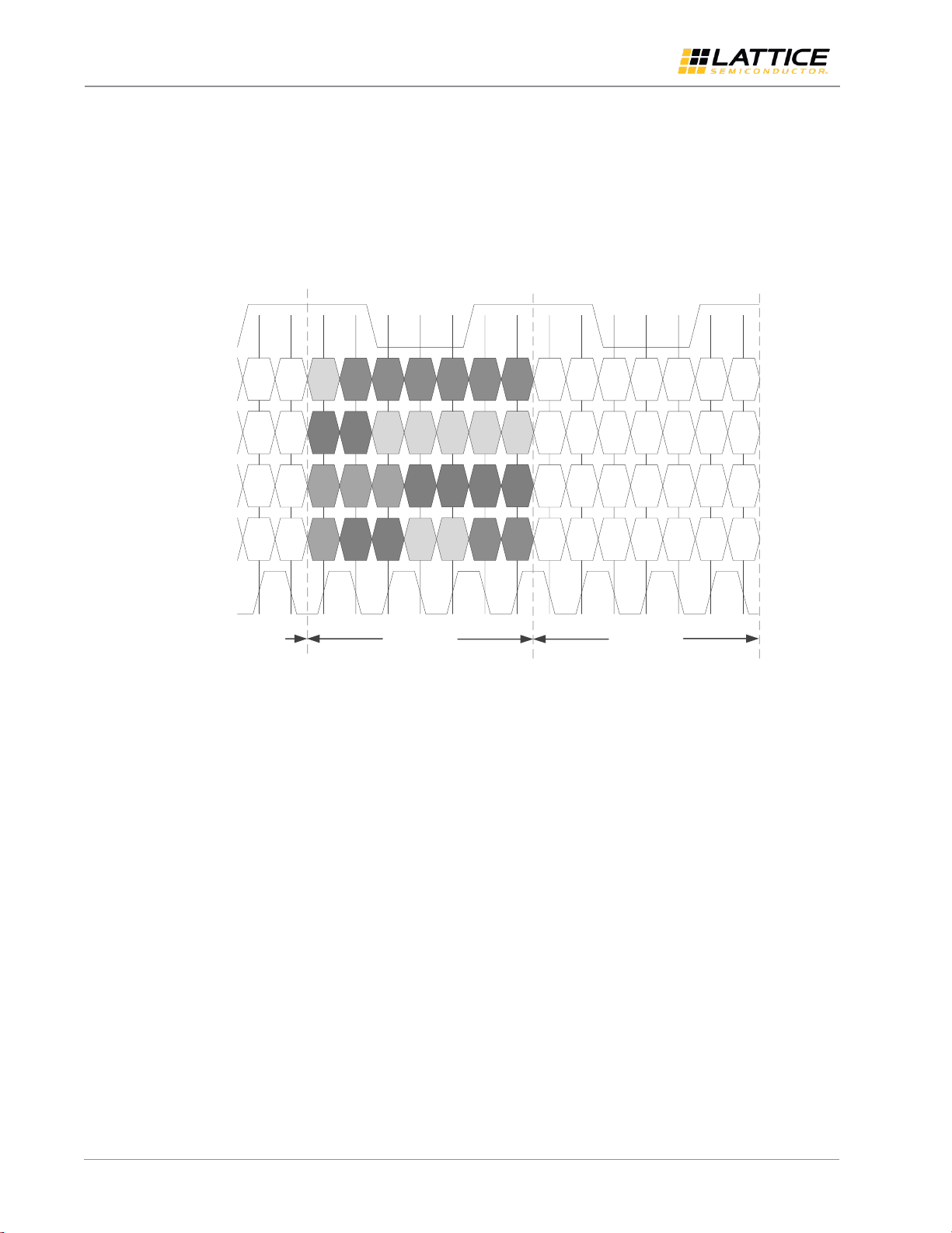
2.1. Interface and Timing Diagrams
Figure 2.2 shows the timing of LVDS 7:1 input interface. There is a 2-bit offset between the rising edge of LVDS clock
and the word boundary. Each word is 7-bit long.
A
DATA0
(n)
A
DATA1
(n)
A
DATA2
(n)
A
DATA3
(n)
A
DATA4
(n)
A
DATA5
(n)
A
DATA6
(n)
CLKIN
DATAIN0
DATAIN1
DATAIN2
DATAIN3
ECLK
A
DATA5
(n-1)
A
DATA6
(n-1)
A
DATA0
(n+1)
A
DATA1
(n+1)
A
DATA2
(n+1)
A
DATA3
(n+1)
A
DATA4
(n+1)
A
DATA5
(n+1)
A
DATA6
(n+1)
B
DATA0
(n)
B
DATA1
(n)
B
DATA2
(n)
B
DATA3
(n)
B
DATA4
(n)
B
DATA5
(n)
B
DATA6
(n)
B
DATA5
(n-1)
B
DATA6
(n-1)
B
DATA0
(n+1)
B
DATA1
(n+1)
B
DATA2
(n+1)
B
DATA3
(n+1)
B
DATA4
(n+1)
B
DATA5
(n+1)
B
DATA6
(n+1)
C
DATA0
(n)
C
DATA1
(n)
C
DATA2
(n)
C
DATA3
(n)
C
DATA4
(n)
C
DATA5
(n)
C
DATA6
(n)
C
DATA5
(n-1)
C
DATA6
(n-1)
C
DATA0
(n+1)
C
DATA1
(n+1)
C
DATA2
(n+1)
C
DATA3
(n+1)
C
DATA4
(n+1)
C
DATA5
(n+1)
C
DATA6
(n+1)
D
DATA0
(n)
D
DATA1
(n)
D
DATA2
(n)
D
DATA3
(n)
D
DATA4
(n)
D
DATA5
(n)
D
DATA6
(n)
D
DATA5
(n-1)
D
DATA6
(n-1)
D
DATA0
(n+1)
D
DATA1
(n+1)
D
DATA2
(n+1)
D
DATA3
(n+1)
D
DATA4
(n+1)
D
DATA5
(n+1)
D
DATA6
(n+1)
Previous
Cycle
Current
Cycle
Next
Cycle
Figure 2.2. OpenLDI/FPD-LINK/LVDS Input Bus Waveform
OpenLDI/FPD-LINK/LVDS Receiver Interface IP
User Guide
© 2017-2019 Lattice Semiconductor Corp. All Lattice trademarks, registered trademarks, patents, and disclaimers are as listed at www.latticesemi.com/legal.
All other brand or product names are trademarks or registered trademarks of their respective holders. The specifications and information herein are subject to change without notice.
10 FPGA-IPUG-02021-1.1
DATAIN0, DATAIN1, DATAIN2, and DATAIN3 are the data lanes. CLKIN is the LVDS clock lane. For every 7-bit data
packet, LSB is the first input serial data to the receiver.
A processor sends video packet data to the FPGA chip via OpenLDI/FPD-LINK (LVDS 7:1) interface. One channel of LVDS
7:1 receiver has a maximum of 5 lanes. Each channel consists of one LVDS clock pair and four LVDS data pairs (RGB888)
or three LVDS data pairs (RGB666). Maximum two LVDS 7:1 channels can be used. When dual channel is selected,
additional data lanes are activated. The clock runs at 1/7th of the data rate, as per the standard for LVDS 7:1 interface.
The default mode for the LVDS operating system is Unbalanced, as this is commonly used. The maximum supported
data rate per lane for LVDS is 1.2 Gb/s.
R1
(n-1) R0
(n-1) G0
(n) R5
(n) R4
(n) R3
(n) R2
(n) R1
(n) R0
(n) G0
(n+1) R5
(n+1) R4
(n+1) R3
(n+1) R2
(n+1)
G2
(n-1) G1
(n-1) B1
(n) B0
(n) G5
(n) G4
(n) G3
(n) G2
(n) G1
(n) B1
(n+1) B0
(n+1) G5
(n+1) G4
(n+1) G3
(n+1)
B3
(n-1) B2
(n-1) DE
(n) Vsync
(n) Hsync
(n) B5
(n) B4
(n) B3
(n) B2
(n) DE
(n+1) Vsync
(n+1) Hsync
(n+1) B5
(n+1) B4
(n+1)
R7
(n-1) R6
(n-1) Rsrv
(n) B7
(n) B6
(n) G7
(n) G6
(n) R7
(n) R6
(n) Rsrv
(n+1) B7
(n+1) B6
(n+1) G7
(n+1) G6
(n+1)
CLKIN
DATAIN0
DATAIN1
DATAIN2
DATAIN3
R1
(n+1) R0
(n+1)
G2
(n+1) G1
(n+1)
B3
(n+1) B2
(n+1)
R7
(n+1) R6
(n+1)
Previous
Cycle
Current
Cycle
Next
Cycle
ECLK
Figure 2.3. Single Channel OpenLDI/FPD-LINK/LVDS Input Bus Waveform for RGB888 Format

OpenLDI/FPD-LINK/LVDS Receiver Interface IP
User Guide
© 2017-2019 Lattice Semiconductor Corp. All Lattice trademarks, registered trademarks, patents, and disclaimers are as listed at www.latticesemi.com/legal.
All other brand or product names are trademarks or registered trademarks of their respective holders. The specifications and information herein are subject to change without notice.
FPGA-IPUG-02021-1.1 11
R1
(n-1) R0
(n-1) G0
(n) R5
(n) R4
(n) R3
(n) R2
(n) R1
(n) R0
(n) G0
(n+1) R5
(n+1) R4
(n+1) R3
(n+1) R2
(n+1)
G2
(n-1) G1
(n-1) B1
(n) B0
(n) G5
(n) G4
(n) G3
(n) G2
(n) G1
(n) B1
(n+1) B0
(n+1) G5
(n+1) G4
(n+1) G3
(n+1)
B3
(n-1) B2
(n-1) DE
(n) Vsync
(n) Hsync
(n) B5
(n) B4
(n) B3
(n) B2
(n) DE
(n+1) Vsync
(n+1) Hsync
(n+1) B5
(n+1) B4
(n+1)
R7
(n-1) R6
(n-1) Rsrv
(n) B7
(n) B6
(n) G7
(n) G6
(n) R7
(n) R6
(n) Rsrv
(n+1) B7
(n+1) B6
(n+1) G7
(n+1) G6
(n+1)
CLKIN
DATAIN0
DATAIN1
DATAIN2
DATAIN3
DATAIN4
DATAIN5
DATAIN6
DATAIN7
Previous
Cycle
Current
Cycle
RL1
(n-1) RL0
(n-1) GL0
(n) RL5
(n) RL4
(n) RL3
(n) RL2
(n) RL1
(n) RL0
(n) GL0
(n+1) RL5
(n+1) RL4
(n+1) RL3
(n+1) RL2
(n+1)
GL2
(n-1) GL1
(n-1) BL1
(n) BL0
(n) GL5
(n) GL4
(n) GL3
(n) GL2
(n) GL1
(n) BL1
(n+1) BL0
(n+1) GL5
(n+1) GL4
(n+1) GL3
(n+1)
BL3
(n-1) BL2
(n-1) Rsrv
(n) CNTLF
(n) CNTLE
(n) BL5
(n) BL4
(n) BL3
(n) BL2
(n) Rsrv
(n+1) CNTLF
(n+1) CNTLE
(n+1) BL5
(n+1) BL4
(n+1)
RL7
(n-1) RL6
(n-1) Rsrv
(n) BL7
(n) BL6
(n) GL7
(n) GL6
(n) RL7
(n) RL6
(n) Rsrv
(n+1) BL7
(n+1) BL6
(n+1) GL7
(n+1) GL6
(n+1)
Next
Cycle
Figure 2.4. Dual Channel OpenLDI/FPD-LINK/LVDS Input Bus Waveform for RGB888 Format
R1
(n-1) R0
(n-1) G0
(n) R5
(n) R4
(n) R3
(n) R2
(n) R1
(n) R0
(n) G0
(n+1) R5
(n+1) R4
(n+1) R3
(n+1) R2
(n+1)
G2
(n-1) G1
(n-1) B1
(n) B0
(n) G5
(n) G4
(n) G3
(n) G2
(n) G1
(n) B1
(n+1) B0
(n+1) G5
(n+1) G4
(n+1) G3
(n+1)
B3
(n-1) B2
(n-1) DE
(n) Vsync
(n) Hsync
(n) B5
(n) B4
(n) B3
(n) B2
(n) DE
(n+1) Vsync
(n+1) Hsync
(n+1) B5
(n+1) B4
(n+1)
CLKIN
DATAIN0
DATAIN1
DATAIN2
R1
(n+1) R0
(n+1)
G2
(n+1) G1
(n+1)
B3
(n+1) B2
(n+1)
Previous
Cycle
Current
Cycle
Next
Cycle
ECLK
Figure 2.5. Single Channel OpenLDI/FPD-LINK/LVDS Input Bus Waveform for RGB666 Format
OpenLDI/FPD-LINK/LVDS Receiver Interface IP
User Guide
© 2017-2019 Lattice Semiconductor Corp. All Lattice trademarks, registered trademarks, patents, and disclaimers are as listed at www.latticesemi.com/legal.
All other brand or product names are trademarks or registered trademarks of their respective holders. The specifications and information herein are subject to change without notice.
12 FPGA-IPUG-02021-1.1
R1
(n-1) R0
(n-1) G0
(n) R5
(n) R4
(n) R3
(n) R2
(n) R1
(n) R0
(n) G0
(n+1) R5
(n+1) R4
(n+1) R3
(n+1) R2
(n+1)
G2
(n-1) G1
(n-1) B1
(n) B0
(n) G5
(n) G4
(n) G3
(n) G2
(n) G1
(n) B1
(n+1) B0
(n+1) G5
(n+1) G4
(n+1) G3
(n+1)
B3
(n-1) B2
(n-1) DE
(n) Vsync
(n) Hsync
(n) B5
(n) B4
(n) B3
(n) B2
(n) DE
(n+1) Vsync
(n+1) Hsync
(n+1) B5
(n+1) B4
(n+1)
CLKIN
DATAIN0
DATAIN1
DATAIN2
DATAIN3
DATAIN4
DATAIN5
DATAIN6
DATAIN7
Previous
Cycle
Current
Cycle
Next
Cycle
RL1
(n-1) RL0
(n-1) GL0
(n) RL5
(n) RL4
(n) RL3
(n) RL2
(n) RL1
(n) RL0
(n) GL0
(n+1) RL5
(n+1) RL4
(n+1) RL3
(n+1) RL2
(n+1)
GL2
(n-1) GL1
(n-1) BL1
(n) BL0
(n) GL5
(n) GL4
(n) GL3
(n) GL2
(n) GL1
(n) BL1
(n+1) BL0
(n+1) GL5
(n+1) GL4
(n+1) GL3
(n+1)
BL3
(n-1) BL2
(n-1) Rsrv
(n) CNTLF
(n) CNTLE
(n) BL5
(n) BL4
(n) BL3
(n) BL2
(n) Rsrv
(n+1) CNTLF
(n+1) CNTLE
(n+1) BL5
(n+1) BL4
(n+1)
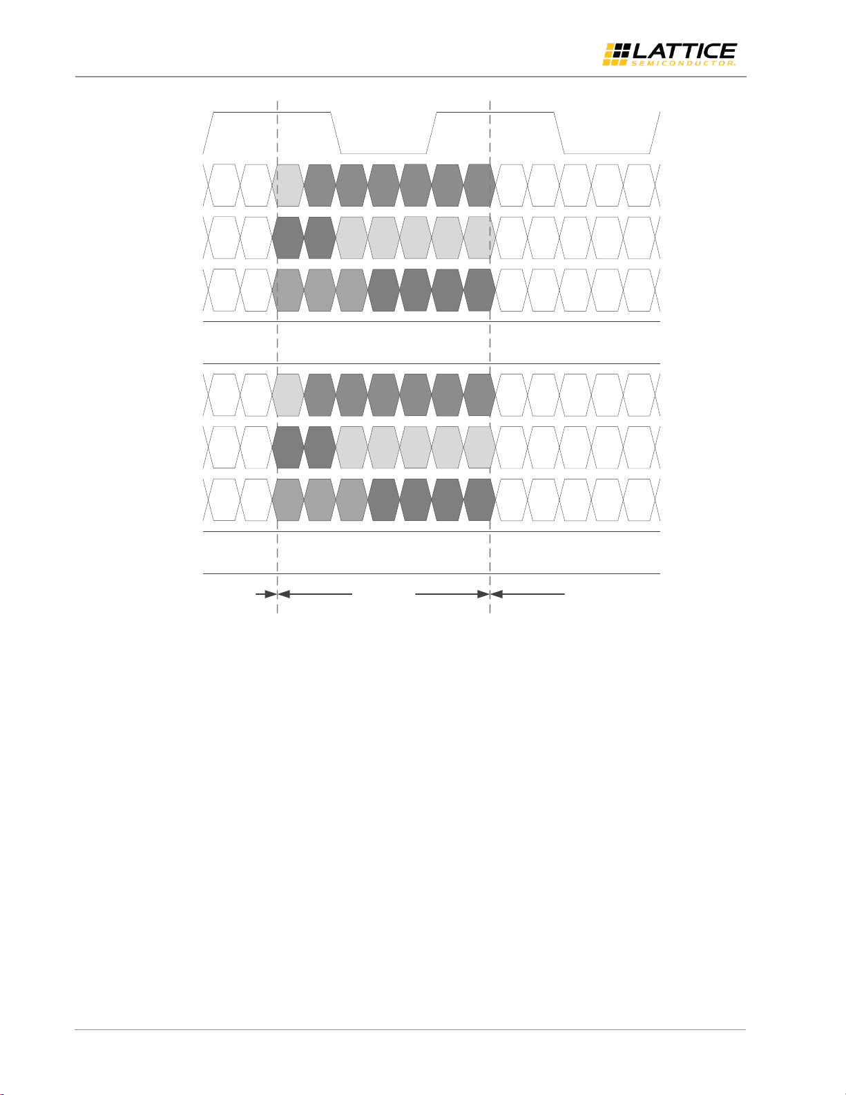
Figure 2.6. Dual Channel OpenLDI/FPD-LINK/LVDS Input Bus Waveform for RGB666 Format
From the processor, data and clock are transmitted serially to the LVDS 7:1 receiver. CrossLink performs data
processing, such as converting the received LVDS serial data to pixel format.
OpenLDI/FPD-LINK/LVDS Receiver Interface IP
User Guide
© 2017-2019 Lattice Semiconductor Corp. All Lattice trademarks, registered trademarks, patents, and disclaimers are as listed at www.latticesemi.com/legal.
All other brand or product names are trademarks or registered trademarks of their respective holders. The specifications and information herein are subject to change without notice.
FPGA-IPUG-02021-1.1 13
A
DATA0
(n)
A
DATA1
(n)
A
DATA2
(n)
A
DATA3
(n)
A
DATA4
(n)
A
DATA5
(n)
A
DATA6
(n)
CLKIN
DATAIN0
DATAIN1
DATAIN2
DATAIN3
ECLK
PIXCLK_OUT
PIXEL_DOUT_0[23:0]
A
DATA5
(n-1)
A
DATA6
(n-1)
A
DATA0
(n+1)
A
DATA1
(n+1)
A
DATA2
(n+1)
A
DATA3
(n+1)
A
DATA4
(n+1)
A
DATA5
(n+1)
A
DATA6
(n+1)
B
DATA0
(n)
B
DATA1
(n)
B
DATA2
(n)
B
DATA3
(n)
B
DATA4
(n)
B
DATA5
(n)
B
DATA6
(n)
B
DATA5
(n-1)
B
DATA6
(n-1)
B
DATA0
(n+1)
B
DATA1
(n+1)
B
DATA2
(n+1)
B
DATA3
(n+1)
B
DATA4
(n+1)
B
DATA5
(n+1)
B
DATA6
(n+1)
C
DATA0
(n)
C
DATA1
(n)
C
DATA2
(n)
C
DATA3
(n)
C
DATA4
(n)
C
DATA5
(n)
C
DATA6
(n)
C
DATA5
(n-1)
C
DATA6
(n-1)
C
DATA0
(n+1)
C
DATA1
(n+1)
C
DATA2
(n+1)
C
DATA3
(n+1)
C
DATA4
(n+1)
C
DATA5
(n+1)
C
DATA6
(n+1)
D
DATA0
(n)
D
DATA1
(n)
D
DATA2
(n)
D
DATA3
(n)
D
DATA4
(n)
D
DATA5
(n)
D
DATA6
(n)
D
DATA5
(n-1)
D
DATA6
(n-1)
D
DATA0
(n+1)
D
DATA1
(n+1)
D
DATA2
(n+1)
D
DATA3
(n+1)
D
DATA4
(n+1)
D
DATA5
(n+1)
D
DATA6
(n+1)
PIXDATA0
(n)
PIXDATA0
(n+1)
A
DATA0
(n+y)
A
DATA1
(n+y)
A
DATA2
(n+y)
A
DATA3
(n+y)
A
DATA4
(n+y)
A
DATA5
(n+y)
A
DATA6
(n+y)
B
DATA0
(n+y)
B
DATA1
(n+y)
B
DATA2
(n+y)
B
DATA3
(n+y)
B
DATA4
(n+y)
B
DATA5
(n+y)
B
DATA6
(n+y)
C
DATA0
(n+y)
C
DATA1
(n+y)
C
DATA2
(n+y)
C
DATA3
(n+y)
C
DATA4
(n+y)
C
DATA5
(n+y)
C
DATA6
(n+y)
D
DATA0
(n+y)
D
DATA1
(n+y)
D
DATA2
(n+y)
D
DATA3
(n+y)
D
DATA4
(n+y)
D
DATA5
(n+y)
D
DATA6
(n+y)
A
DATA0
(n+z)
A
DATA1
(n+z)
A
DATA2
(n+z)
A
DATA3
(n+z)
A
DATA4
(n+z)
A
DATA5
(n+z)
A
DATA6
(n+z)
B
DATA0
(n+z)
B
DATA1
(n+z)
B
DATA2
(n+z)
B
DATA3
(n+z)
B
DATA4
(n+z)
B
DATA5
(n+z)
B
DATA6
(n+z)
C
DATA0
(n+z)
C
DATA1
(n+z)
C
DATA2
(n+z)
C
DATA3
(n+z)
C
DATA4
(n+z)
C
DATA5
(n+z)
C
DATA6
(n+z)
D
DATA0
(n+z)
D
DATA1
(n+z)
D
DATA2
(n+z)
D
DATA3
(n+z)
D
DATA4
(n+z)
D
DATA5
(n+z)
D
DATA6
(n+z)
DE_OUT
VSYNC_OUT
HSYNC_OUT
Figure 2.7. Input to Output Waveform for Single Channel OpenLDI/FPD-LINK/LVDS, Rx Gear 7
A
DATA0
(n)
A
DATA1
(n)
A
DATA2
(n)
A
DATA3
(n)
A
DATA4
(n)
A
DATA5
(n)
A
DATA6
(n)
CLKIN
DATAIN0
DATAIN1
DATAIN2
DATAIN3
ECLK
A
DATA5
(n-1)
A
DATA6
(n-1)
A
DATA0
(n+1)
A
DATA1
(n+1)
A
DATA2
(n+1)
A
DATA3
(n+1)
A
DATA4
(n+1)
A
DATA5
(n+1)
A
DATA6
(n+1)
B
DATA0
(n)
B
DATA1
(n)
B
DATA2
(n)
B
DATA3
(n)
B
DATA4
(n)
B
DATA5
(n)
B
DATA6
(n)
B
DATA5
(n-1)
B
DATA6
(n-1)
B
DATA0
(n+1)
B
DATA1
(n+1)
B
DATA2
(n+1)
B
DATA3
(n+1)
B
DATA4
(n+1)
B
DATA5
(n+1)
B
DATA6
(n+1)
C
DATA0
(n)
C
DATA1
(n)
C
DATA2
(n)
C
DATA3
(n)
C
DATA4
(n)
C
DATA5
(n)
C
DATA6
(n)
C
DATA5
(n-1)
C
DATA6
(n-1)
C
DATA0
(n+1)
C
DATA1
(n+1)
C
DATA2
(n+1)
C
DATA3
(n+1)
C
DATA4
(n+1)
C
DATA5
(n+1)
C
DATA6
(n+1)
D
DATA0
(n)
D
DATA1
(n)
D
DATA2
(n)
D
DATA3
(n)
D
DATA4
(n)
D
DATA5
(n)
D
DATA6
(n)
D
DATA5
(n-1)
D
DATA6
(n-1)
D
DATA0
(n+1)
D
DATA1
(n+1)
D
DATA2
(n+1)
D
DATA3
(n+1)
D
DATA4
(n+1)
D
DATA5
(n+1)
D
DATA6
(n+1)
A
DATA0
(n+y)
A
DATA1
(n+y)
A
DATA2
(n+y)
A
DATA3
(n+y)
A
DATA4
(n+y)
A
DATA5
(n+y)
A
DATA6
(n+y)
B
DATA0
(n+y)
B
DATA1
(n+y)
B
DATA2
(n+y)
B
DATA3
(n+y)
B
DATA4
(n+y)
B
DATA5
(n+y)
B
DATA6
(n+y)
C
DATA0
(n+y)
C
DATA1
(n+y)
C
DATA2
(n+y)
C
DATA3
(n+y)
C
DATA4
(n+y)
C
DATA5
(n+y)
C
DATA6
(n+y)
D
DATA0
(n+y)
D
DATA1
(n+y)
D
DATA2
(n+y)
D
DATA3
(n+y)
D
DATA4
(n+y)
D
DATA5
(n+y)
D
DATA6
(n+y)
A
DATA0
(n+z)
A
DATA1
(n+z)
A
DATA2
(n+z)
A
DATA3
(n+z)
A
DATA4
(n+z)
A
DATA5
(n+z)
A
DATA6
(n+z)
B
DATA0
(n+z)
B
DATA1
(n+z)
B
DATA2
(n+z)
B
DATA3
(n+z)
B
DATA4
(n+z)
B
DATA5
(n+z)
B
DATA6
(n+z)
C
DATA0
(n+z)
C
DATA1
(n+z)
C
DATA2
(n+z)
C
DATA3
(n+z)
C
DATA4
(n+z)
C
DATA5
(n+z)
C
DATA6
(n+z)
D
DATA0
(n+z)
D
DATA1
(n+z)
D
DATA2
(n+z)
D
DATA3
(n+z)
D
DATA4
(n+z)
D
DATA5
(n+z)
D
DATA6
(n+z)
DE_OUT
VSYNC_OUT
HSYNC_OUT
PIXCLK_OUT
PIXEL_DOUT_0[23:0] PIXDATA0
(n)
PIXEL_DOUT_1[23:0] PIXDATA1
(n)
Figure 2.8. Input to Output Waveform for Single Channel OpenLDI/FPD-LINK/LVDS, Rx Gear 14

OpenLDI/FPD-LINK/LVDS Receiver Interface IP
User Guide
© 2017-2019 Lattice Semiconductor Corp. All Lattice trademarks, registered trademarks, patents, and disclaimers are as listed at www.latticesemi.com/legal.
All other brand or product names are trademarks or registered trademarks of their respective holders. The specifications and information herein are subject to change without notice.
14 FPGA-IPUG-02021-1.1
A
DATA0
(n)
A
DATA1
(n)
A
DATA2
(n)
A
DATA3
(n)
A
DATA4
(n)
A
DATA5
(n)
A
DATA6
(n)
CLKIN
DATAIN0
DATAIN1
DATAIN2
DATAIN3
ECLK
PIXCLK_OUT
PIXEL_DOUT_0[23:0]
A
DATA5
(n-1)
A
DATA6
(n-1)
A
DATA0
(n+1)
A
DATA1
(n+1)
A
DATA2
(n+1)
A
DATA3
(n+1)
A
DATA4
(n+1)
A
DATA5
(n+1)
A
DATA6
(n+1)
B
DATA0
(n)
B
DATA1
(n)
B
DATA2
(n)
B
DATA3
(n)
B
DATA4
(n)
B
DATA5
(n)
B
DATA6
(n)
B
DATA5
(n-1)
B
DATA6
(n-1)
B
DATA0
(n+1)
B
DATA1
(n+1)
B
DATA2
(n+1)
B
DATA3
(n+1)
B
DATA4
(n+1)
B
DATA5
(n+1)
B
DATA6
(n+1)
C
DATA0
(n)
C
DATA1
(n)
C
DATA2
(n)
C
DATA3
(n)
C
DATA4
(n)
C
DATA5
(n)
C
DATA6
(n)
C
DATA5
(n-1)
C
DATA6
(n-1)
C
DATA0
(n+1)
C
DATA1
(n+1)
C
DATA2
(n+1)
C
DATA3
(n+1)
C
DATA4
(n+1)
C
DATA5
(n+1)
C
DATA6
(n+1)
D
DATA0
(n)
D
DATA1
(n)
D
DATA2
(n)
D
DATA3
(n)
D
DATA4
(n)
D
DATA5
(n)
D
DATA6
(n)
D
DATA5
(n-1)
D
DATA6
(n-1)
D
DATA0
(n+1)
D
DATA1
(n+1)
D
DATA2
(n+1)
D
DATA3
(n+1)
D
DATA4
(n+1)
D
DATA5
(n+1)
D
DATA6
(n+1)
PIXDATA0
(n)
PIXDATA0
(n+1)
A
DATA0
(n+y)
A
DATA1
(n+y)
A
DATA2
(n+y)
A
DATA3
(n+y)
A
DATA4
(n+y)
A
DATA5
(n+y)
A
DATA6
(n+y)
B
DATA0
(n+y)
B
DATA1
(n+y)
B
DATA2
(n+y)
B
DATA3
(n+y)
B
DATA4
(n+y)
B
DATA5
(n+y)
B
DATA6
(n+y)
C
DATA0
(n+y)
C
DATA1
(n+y)
C
DATA2
(n+y)
C
DATA3
(n+y)
C
DATA4
(n+y)
C
DATA5
(n+y)
C
DATA6
(n+y)
D
DATA0
(n+y)
D
DATA1
(n+y)
D
DATA2
(n+y)
D
DATA3
(n+y)
D
DATA4
(n+y)
D
DATA5
(n+y)
D
DATA6
(n+y)
A
DATA0
(n+z)
A
DATA1
(n+z)
A
DATA2
(n+z)
A
DATA3
(n+z)
A
DATA4
(n+z)
A
DATA5
(n+z)
A
DATA6
(n+z)
B
DATA0
(n+z)
B
DATA1
(n+z)
B
DATA2
(n+z)
B
DATA3
(n+z)
B
DATA4
(n+z)
B
DATA5
(n+z)
B
DATA6
(n+z)
C
DATA0
(n+z)
C
DATA1
(n+z)
C
DATA2
(n+z)
C
DATA3
(n+z)
C
DATA4
(n+z)
C
DATA5
(n+z)
C
DATA6
(n+z)
D
DATA0
(n+z)
D
DATA1
(n+z)
D
DATA2
(n+z)
D
DATA3
(n+z)
D
DATA4
(n+z)
D
DATA5
(n+z)
D
DATA6
(n+z)
E
DATA0
(n)
E
DATA1
(n)
E
DATA2
(n)
E
DATA3
(n)
E
DATA4
(n)
E
DATA5
(n)
E
DATA6
(n)
DATAIN4
DATAIN5
DATAIN6
DATAIN7
E
DATA5
(n-1)
E
DATA6
(n-1)
E
DATA0
(n+1)
E
DATA1
(n+1)
E
DATA2
(n+1)
E
DATA3
(n+1)
E
DATA4
(n+1)
E
DATA5
(n+1)
E
DATA6
(n+1)
F
DATA0
(n)
F
DATA1
(n)
F
DATA2
(n)
F
DATA3
(n)
F
DATA4
(n)
F
DATA5
(n)
F
DATA6
(n)
F
DATA5
(n-1)
F
DATA6
(n-1)
F
DATA0
(n+1)
F
DATA1
(n+1)
F
DATA2
(n+1)
F
DATA3
(n+1)
F
DATA4
(n+1)
F
DATA5
(n+1)
F
DATA6
(n+1)
G
DATA0
(n)
G
DATA1
(n)
G
DATA2
(n)
G
DATA3
(n)
G
DATA4
(n)
G
DATA5
(n)
G
DATA6
(n)
G
DATA5
(n-1)
G
DATA6
(n-1)
G
DATA0
(n+1)
G
DATA1
(n+1)
G
DATA2
(n+1)
G
DATA3
(n+1)
G
DATA4
(n+1)
G
DATA5
(n+1)
G
DATA6
(n+1)
H
DATA0
(n)
H
DATA1
(n)
H
DATA2
(n)
H
DATA3
(n)
H
DATA4
(n)
H
DATA5
(n)
H
DATA6
(n)
H
DATA5
(n-1)
H
DATA6
(n-1)
H
DATA0
(n+1)
H
DATA1
(n+1)
H
DATA2
(n+1)
H
DATA3
(n+1)
H
DATA4
(n+1)
H
DATA5
(n+1)
H
DATA6
(n+1)
E
DATA0
(n+y)
E
DATA1
(n+y)
E
DATA2
(n+y)
E
DATA3
(n+y)
E
DATA4
(n+y)
E
DATA5
(n+y)
E
DATA6
(n+y)
F
DATA0
(n+y)
F
DATA1
(n+y)
F
DATA2
(n+y)
F
DATA3
(n+y)
F
DATA4
(n+y)
F
DATA5
(n+y)
F
DATA6
(n+y)
G
DATA0
(n+y)
G
DATA1
(n+y)
G
DATA2
(n+y)
G
DATA3
(n+y)
G
DATA4
(n+y)
G
DATA5
(n+y)
G
DATA6
(n+y)
H
DATA0
(n+y)
H
DATA1
(n+y)
H
DATA2
(n+y)
H
DATA3
(n+y)
H
DATA4
(n+y)
H
DATA5
(n+y)
H
DATA6
(n+y)
E
DATA0
(n+z)
E
DATA1
(n+z)
E
DATA2
(n+z)
E
DATA3
(n+z)
E
DATA4
(n+z)
E
DATA5
(n+z)
E
DATA6
(n+z)
F
DATA0
(n+z)
F
DATA1
(n+z)
F
DATA2
(n+z)
F
DATA3
(n+z)
F
DATA4
(n+z)
F
DATA5
(n+z)
F
DATA6
(n+z)
G
DATA0
(n+z)
G
DATA1
(n+z)
G
DATA2
(n+z)
G
DATA3
(n+z)
G
DATA4
(n+z)
G
DATA5
(n+z)
G
DATA6
(n+z)
H
DATA0
(n+z)
H
DATA1
(n+z)
H
DATA2
(n+z)
H
DATA3
(n+z)
H
DATA4
(n+z)
H
DATA5
(n+z)
H
DATA6
(n+z)
PIXEL_DOUT_1[23:0] PIXDATA1
(n)
PIXDATA1
(n+1)
DE_OUT
VSYNC_OUT
HSYNC_OUT
Figure 2.9. Input to Output Waveform for Dual Channel OpenLDI/FPD-LINK/LVDS, Rx Gear 7

OpenLDI/FPD-LINK/LVDS Receiver Interface IP
User Guide
© 2017-2019 Lattice Semiconductor Corp. All Lattice trademarks, registered trademarks, patents, and disclaimers are as listed at www.latticesemi.com/legal.
All other brand or product names are trademarks or registered trademarks of their respective holders. The specifications and information herein are subject to change without notice.
FPGA-IPUG-02021-1.1 15
A
DATA0
(n)
A
DATA1
(n)
A
DATA2
(n)
A
DATA3
(n)
A
DATA4
(n)
A
DATA5
(n)
A
DATA6
(n)
CLKIN
DATAIN0
DATAIN1
DATAIN2
DATAIN3
ECLK
A
DATA5
(n-1)
A
DATA6
(n-1)
A
DATA0
(n+1)
A
DATA1
(n+1)
A
DATA2
(n+1)
A
DATA3
(n+1)
A
DATA4
(n+1)
A
DATA5
(n+1)
A
DATA6
(n+1)
B
DATA0
(n)
B
DATA1
(n)
B
DATA2
(n)
B
DATA3
(n)
B
DATA4
(n)
B
DATA5
(n)
B
DATA6
(n)
B
DATA5
(n-1)
B
DATA6
(n-1)
B
DATA0
(n+1)
B
DATA1
(n+1)
B
DATA2
(n+1)
B
DATA3
(n+1)
B
DATA4
(n+1)
B
DATA5
(n+1)
B
DATA6
(n+1)
C
DATA0
(n)
C
DATA1
(n)
C
DATA2
(n)
C
DATA3
(n)
C
DATA4
(n)
C
DATA5
(n)
C
DATA6
(n)
C
DATA5
(n-1)
C
DATA6
(n-1)
C
DATA0
(n+1)
C
DATA1
(n+1)
C
DATA2
(n+1)
C
DATA3
(n+1)
C
DATA4
(n+1)
C
DATA5
(n+1)
C
DATA6
(n+1)
D
DATA0
(n)
D
DATA1
(n)
D
DATA2
(n)
D
DATA3
(n)
D
DATA4
(n)
D
DATA5
(n)
D
DATA6
(n)
D
DATA5
(n-1)
D
DATA6
(n-1)
D
DATA0
(n+1)
D
DATA1
(n+1)
D
DATA2
(n+1)
D
DATA3
(n+1)
D
DATA4
(n+1)
D
DATA5
(n+1)
D
DATA6
(n+1)
A
DATA0
(n+y)
A
DATA1
(n+y)
A
DATA2
(n+y)
A
DATA3
(n+y)
A
DATA4
(n+y)
A
DATA5
(n+y)
A
DATA6
(n+y)
B
DATA0
(n+y)
B
DATA1
(n+y)
B
DATA2
(n+y)
B
DATA3
(n+y)
B
DATA4
(n+y)
B
DATA5
(n+y)
B
DATA6
(n+y)
C
DATA0
(n+y)
C
DATA1
(n+y)
C
DATA2
(n+y)
C
DATA3
(n+y)
C
DATA4
(n+y)
C
DATA5
(n+y)
C
DATA6
(n+y)
D
DATA0
(n+y)
D
DATA1
(n+y)
D
DATA2
(n+y)
D
DATA3
(n+y)
D
DATA4
(n+y)
D
DATA5
(n+y)
D
DATA6
(n+y)
A
DATA0
(n+z)
A
DATA1
(n+z)
A
DATA2
(n+z)
A
DATA3
(n+z)
A
DATA4
(n+z)
A
DATA5
(n+z)
A
DATA6
(n+z)
B
DATA0
(n+z)
B
DATA1
(n+z)
B
DATA2
(n+z)
B
DATA3
(n+z)
B
DATA4
(n+z)
B
DATA5
(n+z)
B
DATA6
(n+z)
C
DATA0
(n+z)
C
DATA1
(n+z)
C
DATA2
(n+z)
C
DATA3
(n+z)
C
DATA4
(n+z)
C
DATA5
(n+z)
C
DATA6
(n+z)
D
DATA0
(n+z)
D
DATA1
(n+z)
D
DATA2
(n+z)
D
DATA3
(n+z)
D
DATA4
(n+z)
D
DATA5
(n+z)
D
DATA6
(n+z)
E
DATA0
(n)
E
DATA1
(n)
E
DATA2
(n)
E
DATA3
(n)
E
DATA4
(n)
E
DATA5
(n)
E
DATA6
(n)
DATAIN4
DATAIN5
DATAIN6
DATAIN7
E
DATA5
(n-1)
E
DATA6
(n-1)
E
DATA0
(n+1)
E
DATA1
(n+1)
E
DATA2
(n+1)
E
DATA3
(n+1)
E
DATA4
(n+1)
E
DATA5
(n+1)
E
DATA6
(n+1)
F
DATA0
(n)
F
DATA1
(n)
F
DATA2
(n)
F
DATA3
(n)
F
DATA4
(n)
F
DATA5
(n)
F
DATA6
(n)
F
DATA5
(n-1)
F
DATA6
(n-1)
F
DATA0
(n+1)
F
DATA1
(n+1)
F
DATA2
(n+1)
F
DATA3
(n+1)
F
DATA4
(n+1)
F
DATA5
(n+1)
F
DATA6
(n+1)
G
DATA0
(n)
G
DATA1
(n)
G
DATA2
(n)
G
DATA3
(n)
G
DATA4
(n)
G
DATA5
(n)
G
DATA6
(n)
G
DATA5
(n-1)
G
DATA6
(n-1)
G
DATA0
(n+1)
G
DATA1
(n+1)
G
DATA2
(n+1)
G
DATA3
(n+1)
G
DATA4
(n+1)
G
DATA5
(n+1)
G
DATA6
(n+1)
H
DATA0
(n)
H
DATA1
(n)
H
DATA2
(n)
H
DATA3
(n)
H
DATA4
(n)
H
DATA5
(n)
H
DATA6
(n)
H
DATA5
(n-1)
H
DATA6
(n-1)
H
DATA0
(n+1)
H
DATA1
(n+1)
H
DATA2
(n+1)
H
DATA3
(n+1)
H
DATA4
(n+1)
H
DATA5
(n+1)
H
DATA6
(n+1)
E
DATA0
(n+y)
E
DATA1
(n+y)
E
DATA2
(n+y)
E
DATA3
(n+y)
E
DATA4
(n+y)
E
DATA5
(n+y)
E
DATA6
(n+y)
F
DATA0
(n+y)
F
DATA1
(n+y)
F
DATA2
(n+y)
F
DATA3
(n+y)
F
DATA4
(n+y)
F
DATA5
(n+y)
F
DATA6
(n+y)
G
DATA0
(n+y)
G
DATA1
(n+y)
G
DATA2
(n+y)
G
DATA3
(n+y)
G
DATA4
(n+y)
G
DATA5
(n+y)
G
DATA6
(n+y)
H
DATA0
(n+y)
H
DATA1
(n+y)
H
DATA2
(n+y)
H
DATA3
(n+y)
H
DATA4
(n+y)
H
DATA5
(n+y)
H
DATA6
(n+y)
E
DATA0
(n+z)
E
DATA1
(n+z)
E
DATA2
(n+z)
E
DATA3
(n+z)
E
DATA4
(n+z)
E
DATA5
(n+z)
E
DATA6
(n+z)
F
DATA0
(n+z)
F
DATA1
(n+z)
F
DATA2
(n+z)
F
DATA3
(n+z)
F
DATA4
(n+z)
F
DATA5
(n+z)
F
DATA6
(n+z)
G
DATA0
(n+z)
G
DATA1
(n+z)
G
DATA2
(n+z)
G
DATA3
(n+z)
G
DATA4
(n+z)
G
DATA5
(n+z)
G
DATA6
(n+z)
H
DATA0
(n+z)
H
DATA1
(n+z)
H
DATA2
(n+z)
H
DATA3
(n+z)
H
DATA4
(n+z)
H
DATA5
(n+z)
H
DATA6
(n+z)
DE_OUT
VSYNC_OUT
HSYNC_OUT
PIXCLK_OUT
PIXEL_DOUT_0[23:0] PIXDATA0
(n)
PIXEL_DOUT_1[23:0] PIXDATA1
(n)
PIXEL_DOUT_2[23:0] PIXDATA2
(n)
PIXEL_DOUT_3[23:0] PIXDATA3
(n)
Figure 2.10. Input to Output Waveform for Dual Channel OpenLDI/FPD-LINK/LVDS, Rx Gear 14
PIXCLK_OUT
PIXEL_DOUT_#[word_width-1:0] {B,G,R}
(n)
{B,G,R}
(n+1)
DE_OUT
Figure 2.11. Output Pixel Data RGB Arrangement

OpenLDI/FPD-LINK/LVDS Receiver Interface IP
User Guide
© 2017-2019 Lattice Semiconductor Corp. All Lattice trademarks, registered trademarks, patents, and disclaimers are as listed at www.latticesemi.com/legal.
All other brand or product names are trademarks or registered trademarks of their respective holders. The specifications and information herein are subject to change without notice.
16 FPGA-IPUG-02021-1.1
Table 2.2. Output Pixel Data Summary
Number of FPD-Link
Channels
Gear
No. of Output Pixel Data
Output Pixel Clock
1
7
1
LVDS input clock
14
2
LVDS input clock/2
2
7
2
LVDS input clock
14
4
LVDS input clock/2
General arrangement on how pixel data are mapped based on configuration are shown in Figure 2.12 and Figure 2.13.
fpd_link_rx
CH 0
GEAR 7
CH1
GEAR 7
P
I
X
4
C
H
0
P
I
X
3
C
H
0
P
I
X
2
C
H
0
P
I
X
1
C
H
0
P
I
X
0
C
H
0
pix_data0_o
pix_data0_o
pix_data0_o
pix_data0_o
pix_data1_o
pix_data2_o
pix_data3_o
fpd_link_rx
CH 0
GEAR 14
CH1
GEAR 14
P
I
X
4
C
H
0
P
I
X
3
C
H
0
P
I
X
2
C
H
0
P
I
X
1
C
H
0
P
I
X
0
C
H
0
pix_data0_o
pix_data1_o
pix_data0_o
pix_data1_o
pix_data2_o
pix_data3_o
Figure 2.12. Output Pixel Data Arrangement for Single Channel OpenLDI/FPD-LINK/LVDS
fpd_link_rx
CH 0
GEAR 14
CH1
GEAR 14
P
I
X
2
C
H
0
P
I
X
1
C
H
1
P
I
X
1
C
H
0
P
I
X
0
C
H
1
P
I
X
0
C
H
0
pix_data0_o
pix_data1_o
pix_data2_o
pix_data3_o
fpd_link_rx
CH 0
GEAR 7
CH1
GEAR 7
P
I
X
2
C
H
0
P
I
X
1
C
H
1
P
I
X
1
C
H
0
P
I
X
0
C
H
1
P
I
X
0
C
H
0
pix_data0_o
pix_data1_o
pix_data0_o
pix_data1_o
pix_data2_o
pix_data3_o
Figure 2.13. Output Pixel Data Arrangement for Dual Channel OpenLDI/FPD-LINK/LVDS

OpenLDI/FPD-LINK/LVDS Receiver Interface IP
User Guide
© 2017-2019 Lattice Semiconductor Corp. All Lattice trademarks, registered trademarks, patents, and disclaimers are as listed at www.latticesemi.com/legal.
All other brand or product names are trademarks or registered trademarks of their respective holders. The specifications and information herein are subject to change without notice.
FPGA-IPUG-02021-1.1 17
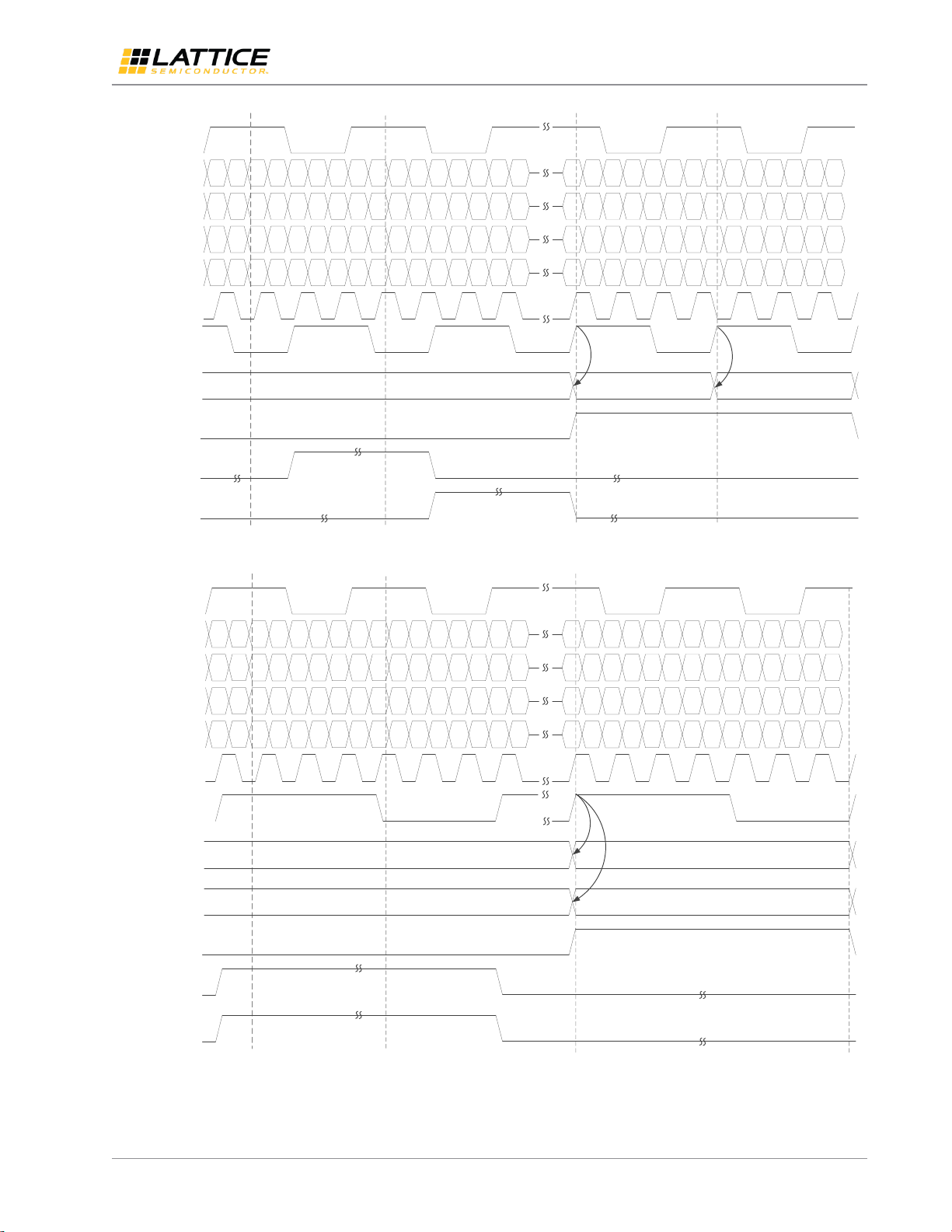
2.2. Clock, Reset and Initialization
2.2.1. Reset and Initialization
Active low reset is used in the design with synchronous release. This is the system reset input connected to LVDS 7:1 Rx
module.
Follow this initialization and reset sequence:
1. Assert active low system reset for at least 500 ns.
2. Wait for GPLL to lock (pll_lock_o) to be asserted. The pll_lock_o is used to indicate that output clock/s of GPLL
is/are already stable.
3. Wait for bw_rdy_o to be asserted. The bw_rdy_o is used to indicate LVDS 7:1 Rx data training is done. Only when
bw_rdy_o is asserted, valid data can be sampled and correctly transmitted by FPD-Link IP.
The LVDS 7:1 Rx Wrapper is now ready to receive valid data.
Note: Steps 2 and 3 are used to make sure that the system is ready to receive valid data. Exact wait time cannot be
specified as the design’s alignment is dynamic and these flag signals are used to observe when to send valid data.
2.2.2. Clock Domains and Clock Domain Crossing
FPD-Link Rx Wrapper
Interface IP
pix_clk_o
FPD-Link Serial Clock
Domain Pixel Clock Domain
clk_ch0_p_i/n_i
Figure 2.14. Clock Domain Crossing Block Diagram
Table 2.3. Clock Domain Crossing
Clock Domain Crossing
Handling Approach
FPD-Link Serial Clock to Pixel Clock
1:7/1:14 gearbox DDR Hard IP
The general formula for computing the required clocks of the IP:
Rx line rate (total) =
Pixclk (Output Pixel Clock) =
Rx LVDS Input Clock =
Rx LVDS ECLK =
Number of Pixels per Pixel Clock =

OpenLDI/FPD-LINK/LVDS Receiver Interface IP
User Guide
© 2017-2019 Lattice Semiconductor Corp. All Lattice trademarks, registered trademarks, patents, and disclaimers are as listed at www.latticesemi.com/legal.
All other brand or product names are trademarks or registered trademarks of their respective holders. The specifications and information herein are subject to change without notice.
18 FPGA-IPUG-02021-1.1
Example:
IP configuration: Single channel FPD-Link Rx, RGB888 data type, 1039.5 Mb/s Rx Line Rate, Rx Gear 7
Rx line rate (total) = =
Pixclk (Internal Pixel Clock) =
=
Rx LVDS Input Clock =
=
Rx LVDS ECLK =
=
Number of Pixels per Pixel Clock =
=
2.3. Design and Module Description
2.3.1. FPD-Link Rx Wrapper Module
The fpd_link_rx_wrapper.v module instantiates fpd_link_rx, general purpose PLL (GPLL), test_mode, lvds71_pxlmap,
and synchronizer modules. The fpd_link_rx module is the core module which performs the data training and serial to
parallel conversion. GPLL is used for fast clock generation. The test_mode is used for internal self-checking.
lvds71_pxlmap is used to decode the output parallel data of fpd_link_rx and convert them into pixel format.
Synchronizers are two-level synchronizers used to sync the system reset into different clock domains before it is used
in the system.
fpd_link_rx_wrapper
CLKFB
RST
CLKOS
PHASEDIR
LOCK
PHASESTEP
PHASELOADREG
CLKOP
CLKI
PHASESEL
GPLL
fpd_link_rx
clk_ch0_i
d0_ch0_i
d1_ch0_i
d2_ch0_i
d3_ch0_i
clk_ch1_i
d0_ch1_i
d1_ch1_i
d2_ch1_i
d3_ch1_i
gsync_rst_i
pixel_clk_o
update_align_i
eclk_i
lock_i
bw_align_phdir_o
bw_align_phstep_o
clkwd_ch0_o
datain0/1/2/3_ch0_i
clkwd_ch1_o
bit_lock_o
word_lock_o
window_size_o
bw_align_rst_i
d0/d1/d2/d3_ch1_o
ready_align_o
ready_gddr_o
sync
lvds71_pxlmap
test_mode
d_i
rst_n_i
clk_i d_o
datain0/1/2/3_ch1_i
test_mode_en_rx_i
pixel_clk_i rst_n_i
comp_en
test_mode_err_o
d0/d1/d2/d3_ch0_o
sync
d_i
rst_n_i
clk_i d_o
d0/d1/d2/d3_ch0_i
d0/d1/d2/d3_ch1_i
pixel_clk_i
de_o
vsync_o
hsync_o
pixel_d0_o
pixel_d1_o
pixel_d2_o
pixel_d3_o
rst_n_i
1'b0
clk_ch0_p_i/n_i
d1_ch0_p_i/n_i
d2_ch0_p_i/n_i
d3_ch0_p_i/n_i
d0_ch0_p_i/n_i
d1_ch1_p_i/n_i
d2_ch1_p_i/n_i
d3_ch1_p_i/n_i
d0_ch1_p_i/n_i
clk_ch1_p_i/n_i
rst_n_i
tstmode_en_i
pll_lock_o
gddr_rdy_o
bw_rdy_o
bit_lock_o
word_lock_o
pix_clk_o
pix_data0_o
pix_data1_o
pix_data2_o
pix_data3_o
hsync_o
vsync_o
de_o
tstmode_err_o
1'b0
1'b1
Figure 2.15. FPD-Link Rx Wrapper Block Diagram

OpenLDI/FPD-LINK/LVDS Receiver Interface IP
User Guide
© 2017-2019 Lattice Semiconductor Corp. All Lattice trademarks, registered trademarks, patents, and disclaimers are as listed at www.latticesemi.com/legal.
All other brand or product names are trademarks or registered trademarks of their respective holders. The specifications and information herein are subject to change without notice.
FPGA-IPUG-02021-1.1 19
2.3.2. FPD-Link Rx Module
The fpd_link_rx module instantiates GDDR_SYNC, BW_ALIGN, several Lattice primitives, and lvds71_ddr_group.v
module. GDDR_SYNC module is required to initialize and synchronize DDR clock and tolerate the large skew between
stop and reset of the DDR components. To properly sample the received data, BW_ALIGN is used to do data training
that includes bit and word alignment with respect to LVDS input clock. Both 1:7 and 1:14 DDR gearing can be used. The
sub-block connection is based on CrossLink GDDR7:1 Rx Usage Model guide.
IDDR71B
SCLK
RST
Q0
ALIGNWD
Q1
Q2
Q3
Q4
Q5
Q6
ECLK
D
IDDR71B
SCLK
RST
Q0
ALIGNWD
Q1
Q2
Q3
Q4
Q5
Q6
ECLK
D
ECLKSYNCB
ECLKI
STOP ECLKO
IDDR71B
SCLK
RST
Q0
ALIGNWD
Q1
Q2
Q3
Q4
Q5
Q6
ECLK
D
IDDR71B
SCLK
RST
Q0
ALIGNWD
Q1
Q2
Q3
Q4
Q5
Q6
ECLK
D
IDDR71B
SCLK
RST
Q0
ALIGNWD
Q1
Q2
Q3
Q4
Q5
Q6
ECLK
D
GDDR_SYNC
RST
SYNC_CLK DDR_RESET
START
STOP
READY CLKDIV
RST CLKI
ALIGNWD CDIVX
ALIGNWD
SYNC_READY
RX_SCLK
UPDATE
RST
PHASESTEP
PHASEDIR
WINDOW_SIZE
RXCLK_WORD[6:0]
BIT_LOCK
WORD_LOCK
READY
BW_ALIGN
d3_ch0/ch1_i
gsync_rst_i
ready_gddr_o
update_align_i
bw_align_rst_i
window_size_o[3:0]
bit_lock_o
word_lock_o
ready_align_o clkwd_ch0/ch1_o[RX_GEAR-1:0]
d3_ch0/ch1_o[RX_GEAR-1:0]
lvds71_ddr_group
pixel_clk_o
d2_ch0/ch1_i
d1_ch0/ch1_i
d0_ch0/ch1_i
d2_ch0/ch1_o[RX_GEAR-1:0]
d1_ch0/ch1_o[RX_GEAR-1:0]
d0_ch0/ch1_o[RX_GEAR-1:0]
pll_lock_i
DELAY_LOADN
DELAY_MOVE
DELAY_DIRECTION
DELAYF
A
LOADN
CFLAG
Z
MOVE
DIRECTION
DELAYF
A
LOADN
CFLAG
Z
MOVE
DIRECTION
DELAYF
A
LOADN
CFLAG
Z
MOVE
DIRECTION
DELAYF
A
LOADN
CFLAG
Z
MOVE
DIRECTION
DELAYF
A
LOADN
CFLAG
Z
MOVE
DIRECTION
clk_ch0_i
clk_ch0_i
eclk_i
bw_align_phstep_o
bw_align_phdir_o
fpd_link_rx
Figure 2.16. FPD-Link Rx Block Diagram
LVDS data are fed to the I/O logic IDDR71 register. LVDS clock is also fed to the I/O logic IDDR71 register, as well as to
PLL. PLL is used to generate the sampling clock (ECLK) which is 3.5 times faster than the LVDS clock. To allow the placing
of the edge of clock in the middle of the data valid window, alignment IP together with PLL is used to shift ECLK to
normally 90 degrees. CLKDIV is used to generate a slower clock (SCLK) which is 3.5 times slower than ECLK. SCLK is
used as the output clock of IDDR71 IP.
After ECLK and SCLK are generated, LVDS 7:1 soft IP performs bit and word alignment. Bit alignment is placing ECLK in
the middle of the data training window, and word alignment is getting the correct training sequence after bit
alignment. Training pattern is 7’b1100011 and alignment is done with respect to LVDS clock. It is expected for the
LVDS clock and data to be edge-aligned with each other, so when alignment is done with respect to the LVDS clock, the
same goes for the LVDS data lanes. Dual x4 LVDS 7:1 Rx can only be supported if the two channels are sharing the same
clock.

OpenLDI/FPD-LINK/LVDS Receiver Interface IP
User Guide
© 2017-2019 Lattice Semiconductor Corp. All Lattice trademarks, registered trademarks, patents, and disclaimers are as listed at www.latticesemi.com/legal.
All other brand or product names are trademarks or registered trademarks of their respective holders. The specifications and information herein are subject to change without notice.
20 FPGA-IPUG-02021-1.1
Table 2.4. FPD-Link Rx Pin List Summary
Port Name
Width
Dir
Type
Description
gsync_rst_i
1
I
LVCMOS
Asynchronous active high reset for GDDR_SYNC.
1 –System on reset
bw_align_rst_i
1
I
LVCMOS
Asynchronous active high reset for BW_ALIGN.
1 –System on reset
eclk_i
1
I
LVCMOS
Fast clock input for ECLKSYNC. Must come from CLKOS of GPLL.
clk_ch0_i
1
I
LVDS
LVDS Input clock to LVDS 7:1 RX Wrapper channel 0.
For all dual channel configuration, only channel 0 clock is used
as reference clock for the system
clk_ch1_i
1
I
LVDS
LVDS Input clock to LVDS 7:1 RX Wrapper channel 1.
For all 2:1 configuration, only channel 0 clock is used as
reference clock for the system, channel 1 clock is unused
d0_ch0_i
1
I
LVDS
LVDS Input data lane 0 to LVDS 7:1 RX Wrapper channel 0
d1_ch0_i
1
I
LVDS
LVDS Input data lane 1 to LVDS 7:1 RX Wrapper channel 0
d2_ch0_i
1
I
LVDS
LVDS Input data lane 2 to LVDS 7:1 RX Wrapper channel 0
d3_ch0_i
1
I
LVDS
LVDS Input data lane 3 to LVDS 7:1 RX Wrapper channel 0
d0_ch1_i
1
I
LVDS
LVDS Input data lane 0 to LVDS 7:1 RX Wrapper channel 1
d1_ch1_i
1
I
LVDS
LVDS Input data lane 1 to LVDS 7:1 RX Wrapper channel 1
d2_ch1_i
1
I
LVDS
LVDS Input data lane 2 to LVDS 7:1 RX Wrapper channel 1
d3_ch1_i
1
I
LVDS
LVDS Input data lane 3 to LVDS 7:1 RX Wrapper channel 1
clkwd_ch0_o
RX_GEAR
O
LVCMOS
Parallel output clkword for channel 0
d3_ ch0_o
RX_GEAR
O
LVCMOS
Parallel output data for lane 3 channel 0
d2_ ch0_o
RX_GEAR
O
LVCMOS
Parallel output data for lane 2 channel 0
d1_ ch0_o
RX_GEAR
O
LVCMOS
Parallel output data for lane 1 channel 0
d0_ ch0_o
RX_GEAR
O
LVCMOS
Parallel output data for lane 0 channel 0
clkwd_ch1_o
RX_GEAR
O
LVCMOS
Parallel output clkword for channel 1
d3_ch1_o
RX_GEAR
O
LVCMOS
Parallel output data for lane 3 channel 1
d2_ch1_o
RX_GEAR
O
LVCMOS
Parallel output data for lane 2 channel 1
d1_ch1_o
RX_GEAR
O
LVCMOS
Parallel output data for lane 1 channel 1
d0_ch1_o
RX_GEAR
O
LVCMOS
Parallel output data for lane 0 channel 1
pixel_clk_o
1
O
LVCMOS
Output clock of LVDS data.
Equivalent to SCLK
update_align_i
1
I
LVCMOS
Active high input to BW_ALIGN module that is used to restart
the bit and word alignment.
(This feature is not used in FPD-Link, always tied to 0)
1 –Restart alignment process
lock_i
1
I
LVCMOS
Starts the GDDR_SYNC process; connected to lock signal of
GPLL.
bw_align_phdir_o
1
O
LVCMOS
Output of BW_ALIGN. Connected to GPLL that is used to
indicate the phase direction for bit and word alignment.
bw_align_phstep_o
1
O
LVCMOS
Output of BW_ALIGN. Connected to GPLL that is used to
indicate the phase step for bit and word alignment.
ready_gddr_o
1
O
LVCMOS
1 –Indicates that DDR synchronization (via GDDR_SYNC) is
done
0 –Indicates that DDR synchronization (via GDDR_SYNC) is still
not started or in progress
ready_align_o
1
O
LVCMOS
1 –Indicates that bit and word alignment are done (via
BW_ALIGN)
0 –Indicates that bit and word alignment is still not started or
in progress (via BW_ALIGN)
Table of contents
Other Lattice Semiconductor Recording Equipment manuals


Popular Recording Equipment manuals by other brands


Calrec
Calrec OMEGA instruction manual

DNA Professional
DNA Professional STUDIO PAD user manual

Campbell
Campbell Campbell Scientific SC532A instruction manual

HMS Networks
HMS Networks Intesis INBACMHI001R000 quick start guide

B&G
B&G DAR-04 Installation and operation manual

Universal Audio
Universal Audio 532 manual