Lattice Semiconductor ECP5 Versa Specification sheet

www.latticesemi.com 1TN1265_1.1
November 2015 Technical Note TN1265
© 2015 Lattice Semiconductor Corp. All Lattice trademarks, registered trademarks, patents, and disclaimers are as listed at www.latticesemi.com/legal. All other brand
or product names are trademarks or registered trademarks of their respective holders. The specifications and information herein are subject to change without notice.
Introduction
ECP5TM and ECP5-5GTM devices support high-speed I/O interfaces, including Double Data Rate (DDR) and Single
Data Rate (SDR) interfaces, using the logic built into the Programmable I/O (PIO). SDR applications capture data
on one edge of a clock while DDR interfaces capture data on both the rising and falling edges of the clock, thus
doubling the performance. ECP5 and ECP5-5G device I/Os also have dedicated circuitry that is used along with
the DDR I/O to support DDR2, DDR3, DDR3L, LPDDR2 and LPDDR3 SDRAM memory interfaces.
This document discusses how to utilize the capabilities of the ECP5 and ECP5-5G devices to implement high-
speed generic DDR interface and the DDR memory interfaces. Refer to the Implementing DDR Memory Interfaces
section of this document for more information.
External Interface Description
This technical note uses two types of external interface definitions, centered and aligned. A centered external inter-
face means that, at the device pins, the clock is centered in the data opening. An aligned external interface means
that, at the device pins, the clock and data transition are aligned. This is also sometimes called edge-on-edge.
Figure 1 shows the external interface waveform for SDR and DDR.
Figure 1. External Interface Definitions
The interfaces described are referenced as centered or aligned interfaces. An aligned interface will need to adjust
the clock location to satisfy the capture flip-flop setup and hold times. A centered interface will need to balance the
clock and data delay to the first flip-flop to maintain the setup and hold already provided.
SDR Aligned
DDR Aligned
SDR Centered
DDR Centered
ECP5 and ECP5-5G
High-Speed I/O Interface

2
ECP5 and ECP5-5G High-Speed I/O Interface
High-Speed I/O Interface BuildingBlocks
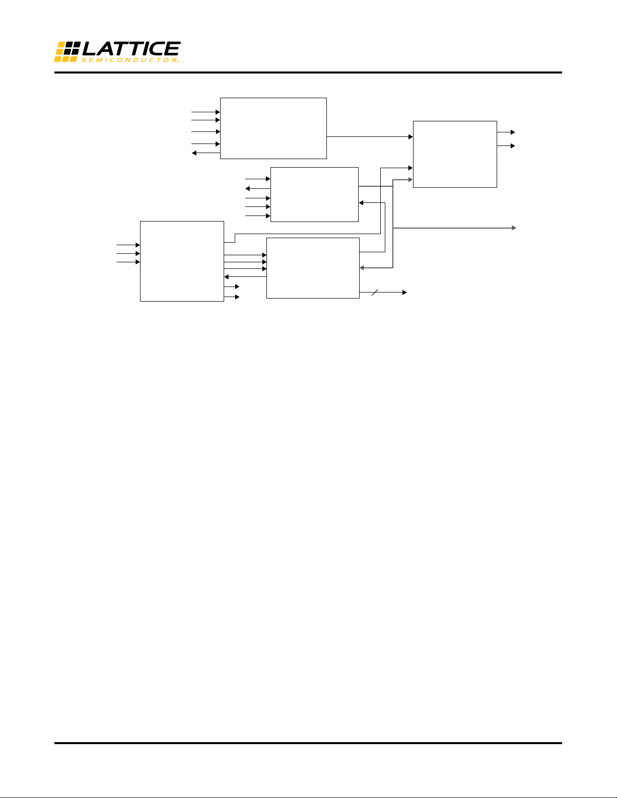
ECP5 and ECP5-5G devices contain dedicated functions for building high-speed interfaces. This section describes
when and how to use these functions. A complete description of the library elements, including descriptions and
attributes, is provided at the end of this document.
Figure 2 shows a high-level diagram of the clocking resources available in the ECP5 and ECP5-5G devices for
building high-speed I/O interfaces.
Figure 2. ECP5 and ECP5-5G Device Clocking Diagram
A complete description of the ECP5 and ECP5-5G device family clocking resources and clock routing restrictions
are available in TN1263, ECP5 and ECP5-5G sysClock PLL/DLL Design and Usage Guide.
Below is a brief description of each of the major elements used for building various high-speed interfaces. The
DDR Software Primitives and Attributes section of this document describes the library elements for these compo-
nents.
Edge Clocks
Edge clocks (ECLK) are high-speed, low-skew I/O dedicated clocks. They are arranged in groups of two per I/O
bank on the left and right sides of the device. Each of these edge clocks can be used to implement a high speed
interface. There is an Edge Clock Bridge (ECLKBRIDGECS) that will allow users to build large interfaces by bridg-
ing the edge clocks from one bank to the other on the same side or from one side to the other side.
Primary Clocks
Primary clocks (PCLK) refer to the system clock of the design. The SCLK ports of the DDR primitives are con-
nected to the system clock of the design.
DQS Lane
A DQS Lane uses the embedded circuit for memory interfaces. Each DQS Lane provides a clock pair (DQSP and
DQSN) for the DQS strobe and up to 12 to 16 ports for DQ data and DM data mask signals. The number of DQS
Lanes on the device is different for each device size. ECP5 and ECP5-5G devices support DQS lanes on the left
and right sides of the device.
Center MUX
Mid
MUX
Mid
MUX
Quadrant TL
Quadrant BL
Quadrant TR
Quadrant BR
GPLL
CLK
DIV
PIOPIOPIOPIO
GPLL
CLK
DIV
PIO PIO PIO PIO
Edge Clocks
Mid
MUX
Edge Clocks
GPLL
CLK
DIV
PIO PIO PIO PIO
GPLL
CLK
DIV
Edge Clocks
Mid
MUX
Edge Clocks
SERDES DCU1
Bank0 Bank1
Bank2 Bank3
Bank6 Bank7
PCSCLKDIV
PCSCLKDIV
SERDES DCU0
Fabric
Entry
Fabric
Entry
Fabric
Entry
Fabric
Entry
14
12
16
Primary Sources Primary Sources
Primary Sources
Primary Sources
Primary
Clocks
Primary
Clocks
Primary
Clocks
Primary
Clocks
16
16
16
16
Bank8
14 DCC 14
14 14 DCC 14
12 DCC
16 DCC
Bank4

3
ECP5 and ECP5-5G High-Speed I/O Interface
PLL
The PLL provides frequency synthesis, with additional static and dynamic phase adjustment, as well. Four output
ports are provided, CLKOP, CLKOS, CLKOS2 and CLKOS3. All four outputs have the same set of dividers. There is
one PLL per corner on the biggest device, totaling to four PLLs on each device.
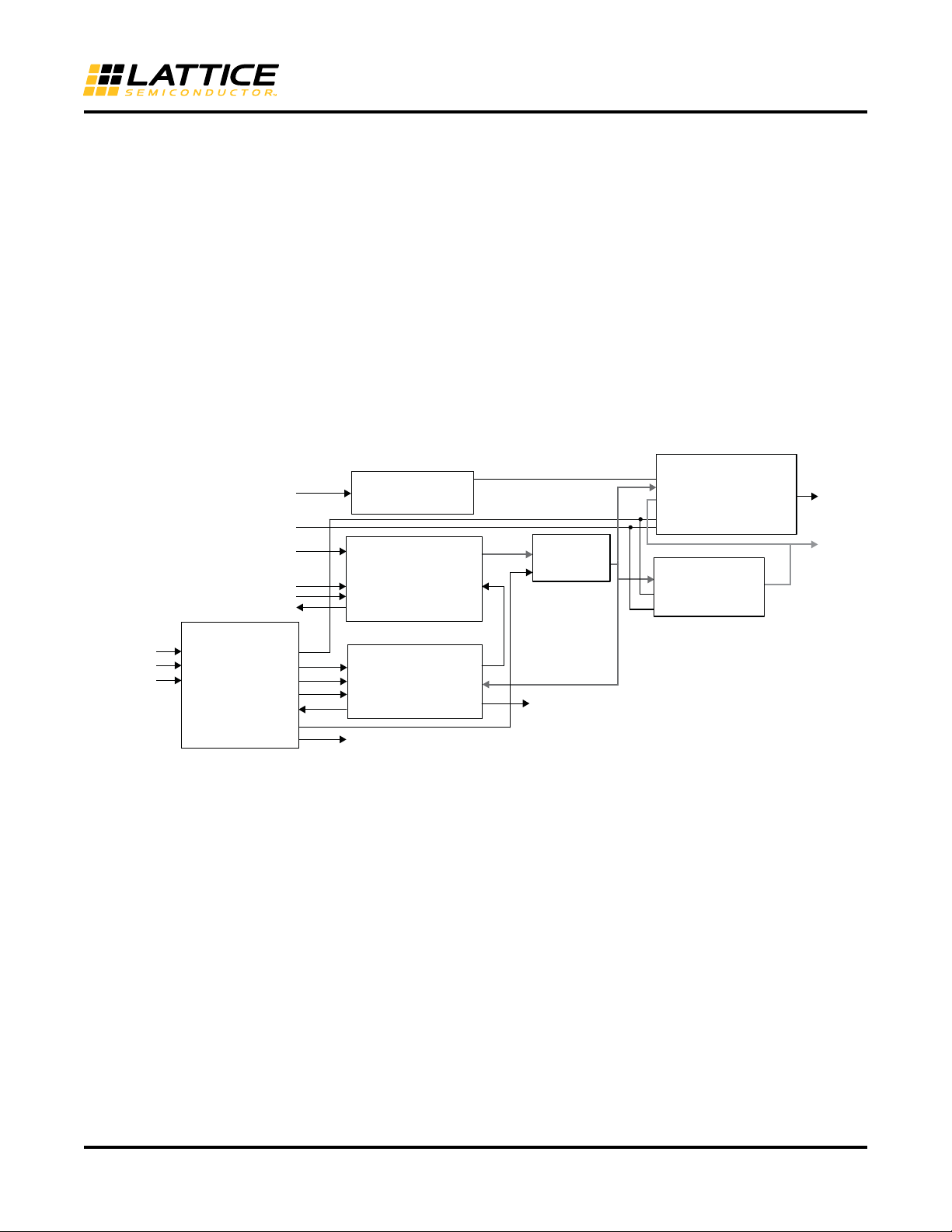
DDRDLL
The DDRDLL is a dedicated DLL for creating the 90° clock delay. The DDRDLL outputs delay codes that are used
in the DQSBUF elements to delay the DQS input or in the DLLDEL module to delay the input clock. There is one
DDRDLL at each corner of the device, totaling to four DDRDLLs on each device. The DDRDLL on the top corners
of the device can drive delay codes to two adjacent edges of the device, providing a possible two DDRDLL codes
for an edge.
Figure 3. DDRDLL Connectivity
DQSBUF
There is one DQSBUF for each DQS lane (every 12 to 16 I/Os depending on the selected device). The DQS input
is used when interfacing to DDR memories. It generates the delay on the DQS pin of the DQS lane, to provide a
90o phase shift on DQS to clock the DDR data at the center. The delay is set by a delay code generated in the
DDRDLL component. Each DQSBUF can receive delay codes from two different DDRDLs hence two different DDR
memory interfaces can be built on one side of the device.
Each of the DQSBUF modes has an additional feature that allows the user to adjust the delay from the delay set by
the DDRDLL code, by using the MOVE and DIRECTION inputs controlled by the user logic. The LOADN will reset
the delay back to the DDRDLL code.
DLLDEL
DLLDEL provides phase shift on the receive side clocks to each ECLK. It functions similar to the DQSBUF, shifting
the clock input by delay set by the DDRDLL delay code, before the clock drives the clock tree. The DLLDEL ele-
ment has the ability to further adjust the delay from the delay set by the DDRDLL code, by using the MOVE and
DIRECTION inputs controlled by the user logic. The LOADN will reset the delay back to the DDRDLL code.
DLLDEL
DLLDEL DLLDEL
DQSBUFDQSBUF
ULC_DDRDLL
LLC_DDRDLL LRC_DDRDLL
URC_DDRDLL

4
ECP5 and ECP5-5G High-Speed I/O Interface
Input DDR (IDDR)
The input DDR function can be used in either 1X (2:1), 2X (4:1) or 7:1 gearing modes. In the 1X mode, the IDDR
module inputs a single DDR data input and SCLK (primary clock) and provides a 2-bit wide data synchronized to
the SCLK (primary clock) to the FPGA fabric.
The 2X gearing is used for interfaces with data rate higher than 400Mbps which would require higher than 200 MHz
system clock. There the IDDR element inputs a single DDR data input and DQS clock (for DDR memory interface)
or Edge Clock ECLK (for all other high speed interfaces) and provides a 4-bit wide parallel data synchronized to
SCLK (primary clock) to the FPGA fabric.
In the 7:1 mode, mostly used in video applications required 7:1 interface, the IDDR element will input a single DDR
data input and ECLK and output a 7 bit wide parallel data synchronized to SCLK (primary clock) to the FPGA fab-
ric.
Output DDR (ODDR)
The output DDR function can also be supported in 1X (2:1), 2X (4:1) or 7:1 gearing modes. In the 1X mode, the
ODDR element receives 2-bit wide data from the FPGA fabric and generates a single DDR data output and Clock
output.
Similar to input interfaces the 2X gearing is used for data rate higher than 400Mbps which would require higher
than 200 MHz system clock. Here the ODDR element receives 4-bit wide data from the FPGA fabric and generates
a single DDR data output and Clock output. The 2X element will use high speed edge clock (ECLK) to clock the
data out for generic high speed interfaces and DQS clock for DDR memory interfaces.
In 7:1 mode, the ODDR element receives 7-bit wide data from FPGA fabric and generates a single DDR data out-
put and Clock output. The 7:1 element will send out data using high speed edge clock.
Edge Clock Dividers (CLKDIV)
Clock dividers are provided to create the divided down clocks used with the I/O Mux/DeMux gearing logic (SCLK
inputs to the DDR) and drives to the Primary Clock routing to the fabric. There are two clock dividers on each side
of the device.
Input/Output DELAY
There are two different types of input/output data delay available. Both DELAYF and DELAYG provide a fixed value
of delay to compensate for clock injection delay. The DELAYF element also allows the delay value to be set by the
user using 128 steps of delay. Each delay step generates ~25ps of delay. In DELAYF, user can overwrite the
DELAY setting dynamically using the MOVE and DIRECTION control inputs. The LOADN will reset the delay back
to the default value.

5
ECP5 and ECP5-5G High-Speed I/O Interface
BuildingGeneric High Speed Interfaces
This section describes in detail on how the high speed interfaces that can be built using the building blocks
described in the section above. The Clarity Designer tool in Lattice Diamond design software will build these inter-
faces based on external interface requirements.
Types of High-Speed DDR Interfaces
This section describes the different types of high-speed DDR interfaces available in ECP5 and ECP5-5G devices.
Table 1 lists these interfaces. Descriptions for each interface in Table 1 are provided below the table.
Table 1. Generic High-Speed I/O DDR Interfaces.
Note: The following describes the naming conventions used for each of the interfaces:
•G–Generic
• IREG – SDR Input I/O Register
• OREG – SDR Output I/O Register
• DDRX1 – DDR 1x gearing I/O Register
• DDRX2 – DDR 2x gearing I/O Registers
• _RX – Receive Interface
• _TX – Transmit Interface
• .ECLK – Uses ECLK (edge clock) clocking resource
• .SCLK – Uses SCLK (primary clock) clocking resource
•.Centered – Clock is centered to the data when coming into the device
Mode Interface Name Description
Receive SDR GIREG_RX.SCLK SDR Input register using SCLK
Receive DDRX1 Aligned GDDRX1_RX.SCLK.Aligned DDR 1x Input using SCLK. Data is edge-to-edge with incoming
clock. DLLDEL will be used to shift the incoming clock
Receive DDRX1 Centered GDDRX1_RX.SCLK.Centered DDR x1 Input using SCLK. Clock is already centered in data window.
Receive DDRX2 Aligned GDDRX2_RX.ECLK.Aligned DDR x2 Input using ECLK. Data is edge-to-edge with incoming
clock. Generic DDR X2 using Edge Clock. DLLDEL will be used to
shift the incoming clock
Receive DDRX2 Centered GDDRX2_RX.ECLK.Centered DDR x2 Input using ECLK. Clock is already centered in data window.
Receive DDRX2 MIPI GDDRX2_RX.MIPI DDRx2 Input using ECLK interfaces to MIPI interface. This will use
additional IMIPI module for the interface.
Receive DDRX71 GDDRX71_RX.ECLK DDR 7:1 input using ECLK.
Transmit SDR GOREG_TX.SCLK SDR Output using SCLK. Clock is forwarded through ODDR.
TX DDRX1 Aligned GDDRX1_TX.SCLK.Aligned DDR x1 Output using SCLK. Data is edge-on-edge using same
clock through ODDR.
TX DDRX1 Centered GDDRX1_TX.SCLK.Centered DDR x1 Output using SCLK. Clock is centered using PLL with dif-
ferent SCLK.
TX DDRX2 Aligned GDDRX2_TX.ECLK.Aligned DDR x2 Output that is edge-on-edge using ECLK.
TX DDRX2 Centered GDDRX2_TX.ECLK.Centered DDR x2 Output that is pre-centered PLL generated 90o phase, and
output on ECLKs.
TX DDRX71 GDDRX71_TX.ECLK DDR 7:1 output using ECLK. Data and CLK are aligned on first of 7
bits.

6
ECP5 and ECP5-5G High-Speed I/O Interface
High-Speed DDR Interface Details
This section describes each of the generic high-speed interfaces in detail, including the clocking to be used for
each interface. For detailed information about the ECP5 and ECP5-5G device clocking structure, refer to TN1263,
ECP5 and ECP5-5G sysClock PLL/DLL Design and Usage Guide. The various interface rules listed under each
interface should be followed to build these interfaces successfully. Refer to the Timing Analysis for High Speed
DDR Interfaces section of this document for more information about the timing analysis on these interfaces.
Some of these interfaces may require a soft IP in order utilize all the features available in the hardware. These soft
IP cores are available in Clarity Designer and are described in this section. Some of the soft IPs are optional and
can be selected in the Clarity Designer. Some of these are mandatory for the module to function as expected and
will automatically be generated when building the interface through Clarity Designer.
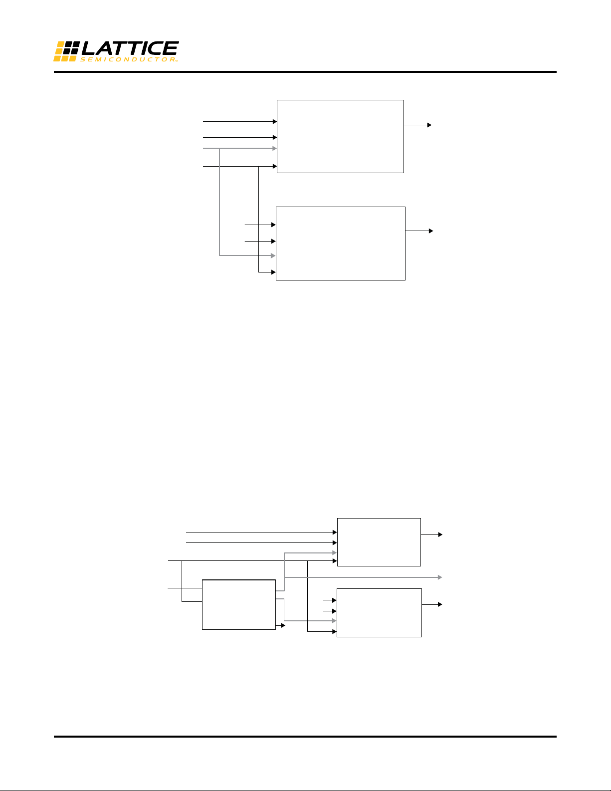
GDDRX1_RX.SCLK.Centered
This a Generic 1X gearing Receive interface using SCLK. The clock is coming in centered to the Data. This inter-
face must be used for speeds below 200 MHz.
This DDR interface uses the following modules:
• IDDRX1F element to capture the data
• The incoming clock is routed through the Primary (SCLK) clock tree
• Static data delay element DELAYG is used to delay the incoming data enough to remove the clock injection time.
• Optionally the user can choose to use Dynamic Data delay adjustment using DELAYF element to control the
delay on the DATA dynamically. DELAYF will also allow user to override the input delay set. The type of delay
required can be selected through Clarity Designer.
• DEL_MODE attribute is used with DELAYG and DELAYF element to indicate the interface type so that the cor-
rect delay value can be set in the delay element.
The following figures show the static delay and dynamic delay options for this interface.
Figure 4. GDDRX1_RX.SCLK.Centered Interface (Static Delay)
Figure 5. GDDRX1_RX.SCLK.Centered Interface (Dynamic Data delay)
IDDRX1F
SCLK
DQ0
Q1
RST
AO
DELAYG
Z
Datain Q[0]
Q[1]
Clkin
Reset
DEL_MODE =
SCLK_CENTERED
Sclk
IDDRX1F
SCLK
DQ0
Q1
RST
Datain
Reset
Q[0]
Q[1]
Z
ADELAYF
LOADN
MOVE
DIRECTION
Z
data_cflag
data_loadn
data_move
data_direction
Clkin
(Optional)
DEL_MODE=SCLK_CENTERED
Sclk

7
ECP5 and ECP5-5G High-Speed I/O Interface
Interface Requirements
• The clock input must use a PCLK input so that it can be routed directly to the primary clock tree.
• The user must set the timing preferences as per section “Timing Analysis Requirement”
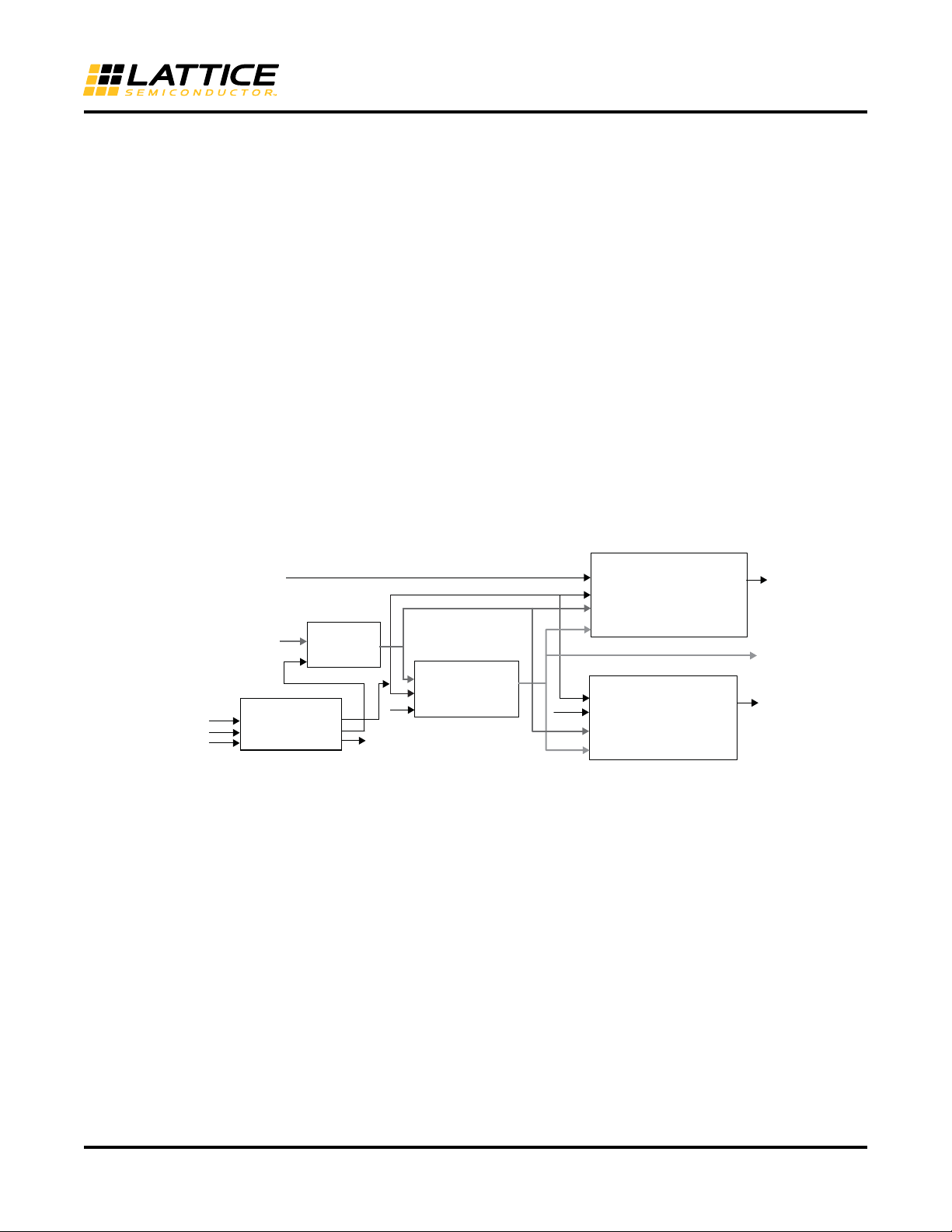
GDDRX1_RX.SCLK.Aligned
This a Generic 1X gearing Receive interface using SCLK. The clock is coming in edge aligned to the Data. This
interface must be used for speeds below 250 MHz.
This DDR interface uses the following modules:
• IDDRX1F element to capture the data
• DDRDLLA/DLLDELD blocks are used to phase shift the incoming clock going to primary clock tree (SCLK)
• Static data delay element DELAYG is used to delay the incoming data enough to remove the clock injection time.
• Optionally the user can choose to use Dynamic Data delay adjustment using DELAYF element to control the
delay on the DATA dynamically. DELAYF will also allow user to override the input delay set. The type of delay
required can be selected through Clarity Designer
• DEL_MODE attribute is used with DELAYG and DELAYF element to indicate the interface type so that the cor-
rect delay value can be set in the delay element.
• Dynamic Margin adjustment in the DDRDLLA module can be optionally used to adjust the DDRDLLA delay
dynamically
The output of the DLLDELD module is also used as the clock input to the DDRDLLA which sends the delay values
to the DLLDELD module. The Receiver Synchronization (RX_SYNC) soft IP is required for the aligned interfaces to
prevent stability issues that may occur due to this loop at startup. The soft IP will prevent any updates to the DLL-
DELD at start until the DDRDLLA is locked. Once locked the DLLDELD is updated and FREEZE on the DDRDLL is
removed. This soft IP will be automatically generated by Clarity Designer.
The following figures show the static delay and dynamic delay options for this interface.
Figure 6. GDDRX1_RX.SCLK.Aligned Interface (Static Delay)
IDDRX1F
SCLK
DQ0
Q1
RST
Datain Q[0]
Q[1]
Clkin
A
DELAYG
Z
DLLDELD
Z
A
DDRDEL
LOADN
MOVE
DIRECTION
CFLAG
CLK
RST
UDDCNTLN
FREEZE
DDRDEL
LOCK
DDRDLLA
DCNTL[7:0]
“0”
“0”
(open)
Primary
DEL_MODE =
SCLK_ALIGNED
Ready
STOP
DLL_LOCK
FREEZE
UDDCNTLN
DLL_RESET
DDR_RESET
SYNC_CLK
RST
UPDATE
Sync_clk
Sync_reset
Update
READY
(open)
RX_SYNC Sclk
Dcntl[7:0]
8
ECP5 and ECP5-5G High-Speed I/O Interface
Figure 7. GDDRX1_RX.SCLK.Aligned Interface (Dynamic Data/Clock Delay)
Interface Requirements
• The clock input must use a PCLK input so that it can be routed directly to the DLLDELD input
• The user must set the timing preferences as per section “Timing Analysis Requirement”
GDDRX2_RX.ECLK.Centered
Generic Receive DDR with the 2X gearing using Edge Clock Tree (ECLK). Input clock is centered to the input Data.
This interface must be used for speeds above 200 MHz.
This DDR interface uses the following modules:
• IDDRX2F element for X2 mode to capture the data
• The incoming clock is routed to the Edge clock (ECLK) clock tree through the ECLKSYNCB module
• CLKDIVF module is used to divide the incoming clock by 2 to generate the SCLK
• Static data delay element DELAYG to delay the incoming data enough to remove the clock injection time
• Optionally the user can choose to use Dynamic Data delay adjustment using DELAYF element to control the
delay on the DATA dynamically. DELAYF will also allow user to override the input delay set. The type of delay
required can be selected through Clarity Designer
• DEL_MODE attribute is used with DELAYG and DELAYF element to indicate the interface type so that the cor-
rect delay value can be set in the delay element
• The ECLKBRIDGE can be optionally enabled if the data bus will be crossing over between the left and right sides
of the device. If ECLKBRIDGE is enabled then the ECLKBRIDGECS element should be used in the interface
before the ECLKSYNCB element. This element can be enabled through Clarity Designer.
• The startup synchronization soft IP (GDDRX_SYNC) is required for this interface to tolerate the skew between
the ECLKSYNCB Stop input and the Reset to the DDR and CLKDIV modules.
The following figures show the static delay and dynamic delay options for this interface.
Data_LoadN
Data_Move
Data_Direction
A
DELAYF
LOADN
MOVE
DIRECTION
CFLAG
Datain
Q[0]
Q[1]
Clkin DLLDELD
Z
A
DDRDEL
LOADN
MOVE
DIRECTION
CFLAG
IDDRX1F
SCLK
DQ0
Q1
RST
CLK
RST
UDDCNTLN
FREEZE
DDRDEL
LOCK
DDRDLLA
DCNTL[7:0] Dcntl[7:0]
Clock_LoadN
Clock_Move
Clock_Direction
Clock_CFlag
Data_CFlag
7
Z
Primary
(optional)
DEL_MODE=
SCLK_ALIGNED
STOP
DLL _LOCK
FREEZE
UDDCNTLN
DLL _RESET
DDR _RESET
SYNC_CLK
RST
UPDATE
Sync_clk
sync_reset
Update
READY
(open)
RX_SYNC
(soft IP)
Sclk

9
ECP5 and ECP5-5G High-Speed I/O Interface
Figure 8. GDDRX2_RX.ECLK.Centered Interface (Static Delay)
Figure 9. GDDRX2_RX.ECLK.Centered Interface (Dynamic Data Delay)
Interface Requirements
• The clock input must use a PCLK input so that it can be routed directly to the edge clock tree.
• ECLK must use the Edge clock tree and the SCLK out of the CLKDIVF must use the Primary clock tree, software
will error out if these dedicated clock routes are not used
• “USE PRIMARY” preference may be assigned to the SCLK net
• The user must set the timing preferences as per section “Timing Analysis Requirement”
GDDRX2_RX.ECLK.Aligned
Generic Receive DDR with the 2X gearing with ECLK. Input Clock is coming in edge aligned to the Data. This inter-
face must be used for speeds above 20 MHz.
This DDR interface uses the following modules:
• IDDRX2F element for 2X mode to capture the data
• DDRDLLA/DLLDELD blocks are used to phase shift the incoming clock routed to the Edge clock (ECLK) clock
tree through the ECLKSYNCB module
• CLKDIVF module is used to divide the incoming clock by 2
• Static data delay element DELAYG to delay the incoming data enough to remove the clock injection time
• Optionally the user can choose to use Dynamic Data delay adjustment using DELAYF element to control the
delay on the DATA dynamically. DELAYF will also allow user to override the input delay set. The type of delay
required can be selected through Clarity Designer
ALIGNWD
Datain
Clkin
A
DELAYG Z
ECLKI
STOP ECLKO
SCLK
D
Q[3:0]
RST
ALIGNWD
ECLK
IDDRX2F
Edge
Primary Sclk
CLKDIVF
CLKI
RST
CDIVX
AlignWD
Q[3:0]
ECLKSYNCB
DEL_MODE=
ECLK_CENTERED
sync_reset
GDDR _SYNC
Sync _clk
Start
RST
START
SYNC_CLK
DDR_RESET
STOP
READY Ready
Data_LoadN
Data_Move
Data_Direction
A
DELAYF
LOADN
MOVE
DIRECTION
CFLAG
Datain
Data_CFlag
Z
ECLKI
STOP ECLKO
SCLK
D
RST
ALIGNWD
ECLK
Edge
Primary
Sclk
CLKDIVF
CLKI
RST
ALIGNWD
CDIVX
AlignWD
Clkin
Q[3:0] Q[3:0]
IDDRX2F
ECLKSYNCB
sync_reset
GDDR_SYNC
Sync_clk
Start
RST
START
SYNC_CLK
DDR_RESET
STOP
READY Ready
DEL_MODE=
ECLK_CENTERED
10
ECP5 and ECP5-5G High-Speed I/O Interface
• DEL_MODE attribute is used with DELAYG and DELAYF element to indicate the interface type so that the cor-
rect delay value can be set in the delay element
• The ECLKBRIDGE can be optionally enabled if the data bus will be crossing over between the left and right sides
of the device. If ECLKBRIDGE is enabled then the ECLKBRIDGECS element should be used in the interface
before the ECLKSYNCB element. This element can be enabled through Clarity Designer.
• Dynamic Margin adjustment in the DDRDLLA module can be optionally used to adjust the DDRDLLA delay
dynamically
The output of the DLLDELD module is also used as the clock input to the DDRDLLA which sends the delay values
to the DLLDELD module. The Receiver Synchronization (RX_SYNC) soft IP is required for the aligned interfaces to
prevent stability issues that may occur due to this loop at startup. The soft IP will prevent any updates to the DLL-
DELD at start until the DDRDLLA is locked. Once locked the DLLDELD is updated and FREEZE on the DDRDLL is
removed. This soft IP will be automatically generated by Clarity Designer.
The following figures show the static delay and dynamic delay options for this interface.
Figure 10. GDDRX2_RX.ECLK.Aligned Interface (Static Delay)
Datain
Clkin
A
DELAYG Z
DLLDELD
Z
A
DDRDEL
LOADN
MOVE
DIRECTION
CFLAG
CLK
RST
UDDCNTLN
FREEZE
DDRDEL
LOCK
DDRDLLA
DCNTL[7:0]
“0”
“0”
(open )
ECLKI
STOP ECLKO
SCLK
D
RST
ALIGNWD
ECLK
Edge
Primary
CLKDIVF
CLKI
RST
ALIGNWD
CDIVX
alignwd
IDDRX2F
Q[3:0] Q[3:0]
ECLKSYNCB
dcntl[7:0]
STOP
DLL_LOCK
FREEZE
UDDCNTLN
DLL_RESET
DDR_RESET
SYNC_CLK
RST
UPDATE
Sync_clk
sync_reset
Update
READY Ready
RX_SYNC
DEL_MODE=
ECLK_CENTERED
Sclk

11
ECP5 and ECP5-5G High-Speed I/O Interface
Figure 11. GDDRX2_RX.ECLK.Aligned Interface (Dynamic Data/Clock Delay)
Interface Requirements
• The clock input must use a dedicated PCLK input so that it can be routed directly to the DLLDEL module
• ECLK must use the Edge clock tree and the SCLK out of the CLKDIVD must use the Primary clock tree, software
will error out if these dedicated clock routes are not used
• “USE PRIMARY” preference may be assigned to the SCLK net
• The user must set the timing preferences as per section “Timing Analysis Requirement”
GDDRX2_RX.MIPI
Generic Receive DDR for MIPI interfaces using the X2 gearing with ECLK. Clock is coming in centered to the Data.
This interface must be used for speeds above 200 MHz.
This DDR interface uses the following modules:
• IMIPI element use to receive the MIPI data and clock
• The HSSEL of the IMIPI is used to switch between the High speed and Low Speed modes
• The HSSEL of IMIPI should be driven by a soft IP
• When in high speed mode
– The OHSOLS1 of the element is active
– The OHSOLS1 of the data IMIPI element is connected to the Data input GDDRX2_RX.ECLK.Centered
Interface
– The OHSOLS1 of the clock IMIPI is connected to the ECLK input GDDRX2_RX.ECLK.Centered Interface
– This is then treated similar to the GDDRX2_RX.ECLK.Centered Interface
• When in low speed mode:
– Both the outputs of IMIPI are active since it is not a 2-bit interface
– The OHSLS1 is the bit 1 and OLS0 is the bit 0 of the interface.
– Each of the data input and clock input is connected through a 20ns filter soft IP to the core
Data_LoadN
Data_Move
Data_Direction
A
DELAYF
LOADN
MOVE
DIRECTION
CFLAG
Datain
Clkin
DDR_reset
DLLDELD Z
A
DDRDEL
LOADN
MOVE
DIRECTION
CFLAG
CLK
RST
UDDCNTLN
FREEZE
DDRDEL
LOCK
DDRDLLA
DCNTL[7:0] Dcntl[7:0]
Clock_LoadN
Clock_Move
Clock_Direction
Clock_CFlag
Data_CFlag
Z
ECLKI
STOP
ECLKO
SCLK
D
RST
ALIGNWD
ECLK
Edge
Primary
Sclk
CLKDIVF
CLKI
RST
ALIGNWD
CDIVX
AlignWD
Q[3:0] Q[3:0]
IDDRX2F
ECLKSYNCB
(optional)
STOP
DLL_LOCK
FREEZE
UDDCNTLN
DLL_RESET
DDR_RESET
SYNC_CLK
RST
UPDATE
Sync_clk
Sync_rst
Update
READY
RX_SYNC
Ready
DEL_MODE=
ECLK_CENTERED

12
ECP5 and ECP5-5G High-Speed I/O Interface
• The ECLKBRIDGE can be optionally enabled if the data bus will be crossing over between the left and right sides
of the device. If ECLKBRIDGE is enabled then the ECLKBRIDGECS element should be used in the interface
before the ECLKSYNCB element. This element can be enabled through Clarity Designer.
Figure 12. GDDRX2_RX.MIPI
Interface Requirements
• The clock input must use a PCLK input so that it can be routed directly to the edge clock tree.
• ECLK must use the Edge clock tree and the SCLK out of the CLKDIVF must use the Primary clock tree, software
will error out if these dedicated clock routes are not used
• “USE PRIMARY” preference may be assigned to the SCLK net
• The user must set the timing preferences as per section “Timing Analysis Requirement”
GDDRX71_RX.ECLK
This interface is used to implement 7:1 LVDS Receiver interface using the 1 to 7 gearing with ECLK. Slow speed
clock coming in is multiplied 3.5X using a PLL. This clock is used to capture the data at the receiver IDDRX71 mod-
ule.
This DDR interface uses the following modules:
• IDDRX71B element is used to capture the data
• EHXPLLK will multiply the input clock by 3.5 and phase shift the incoming clock based on the dynamic phase
shift input.
• This clock is routed to the Edge clock (ECLK) clock tree through the ECLKSYNCB module
• CLKDIVF module is used to divide the ECLK by 3.5 and is routed to the primary clock tree used as the SCLK
input
• A second IDDRX71B element is used with data connected to clock input to generate 7 bit clock phase that can
be used for word alignment
• The startup synchronization soft IP (GDDRX_SYNC) is required for this interface to tolerate the skew between
the ECLKSYNCB Stop input and the Reset to the DDR and CLKDIV modules.
• An optional Bit and Word alignment soft IP(BW_ALIGN) can be enabled in Clarity Designer. The Bit alignment
module will rotate PLL’s 16 phases to center Edge clock to middle of data eye and the word alignment module will
use ALIGNWD function of CLKDIVD and IDDRX71B to achieve 7-bit word alignment
• The ECLKBRIDGE can be optionally enabled if the data bus will be crossing over between the left and right sides
of the device. If ECLKBRIDGE is enabled then the ECLKBRIDGECS element should be used in the interface
before the ECLKSYNCB element. This element can be enabled through Clarity Designer.
Dat a_P
Dat a_N
hsdatasel
ALI GNWD
A
DELAYG Z
ECLKI
STOP ECLKO
SCLK
D
Q[3:0]
ST
ALIGNWD
ECLK
IDDRX2F
Primary Sclk
CLKDIVF
CLKI
RST CDIVX
Alignwd
Q[3:0]
ECLKSYNCB
DEL_MODE=
ECLK_CENTERED
A
AN
HSSEL OLSO0
A
AN
HSSEL
OHSOLS1
Clk_P
Clk_N
hsclksel
ALIGNWD
sync_reset
GDDR_SYNC
Sync_clk
Start
RST
START
SYNC_CLK
DDR_RESET
STOP
READY Ready
OLS0
OHSOLS1
Edge
lsdatain[1]
lsdatain[0]
lsclkin[0]
lsclkin[1]

13
ECP5 and ECP5-5G High-Speed I/O Interface
The following figures show the interface with the soft IP modules.
Figure 13. GDDRX71_RX.ECLK Interface
Interface Requirements
• The clock input must use a dedicated PLL input pin so it is routed directly to the PLL
• CLKOP output of the PLL must be used as feedback using another edge clock tree to compensate for ECLK tree
delay used by CLKOS. Hence this interface will use two ECLK trees.
• ECLK must use the Edge clock tree and the SCLK out of the CLKDIVF must use the Primary clock tree.
• “Use Primary” preference may be assigned to the SCLK out of the CLKDIVF module
GDDRX1_TX.SCLK.Aligned
This interface is used to implement Generic Transmit DDR with 1X gearing using primary clock (SCLK). The Clock
output is aligned to the Data output.
This DDR interface uses the following modules:
• ODDRX1F element is used to generate the data output
• The primary clock (SCLK) is used as the clock for both data and clock generation
• Optionally the user can choose to use the DELAYG or DELAYF element to delay the output data
• The output data can be optionally tristated using either a Tristate input going through an I/O register.
Datain
Clkin
EHXPLLL CLKOP
CLKI
PHASESEL
PHASEDIR
RST ECLKI
STOP ECLKO
Edge
Primary
sclk
CLKDIVF
CLKI
RST
ALIGNWD
CDIVX
(divby 3.5)
CLKFB
CLKOS
LOCK
PHASESTEP
SCLK
DQ0
Q1
RST
ALIGNWD
ECLK Q2
Q3
Q4
Q5
Q6
IDDR71B
SCLK
DQ0
Q1
RST
ALIGNWD
ECLK Q2
Q3
Q4
Q5
Q6
IDDR 71 B Q[0]
Q[1]
Q[2]
Q[3]
Q[4]
Q[5]
Q[6]
Edge
ECLKSYNCB
clock _phase [ 6 :0 ]
pll _reset
Sync_reset
GDDR _SYNC
Sync_clk
RST
START
SYNC_CLK
DDR_RESET
STOP
READY
Ready
RX_ SCLK
RXCLK_
WORD<6:0>
UPDATE
PLL_LOCK
RST
PHASESTEP
PHASEDIR
ALIGNWORD
WINDOW_SIZE
BIT_ LOCK
WORD_LOCK
READY Align_ready
Update
Bw_align_Rst
Window_size
Bit_lock
Word_lock
ECLKI
STOP
ECLKO
ECLKSYNCB
“0”
PHASELOADREG
“1”
14
ECP5 and ECP5-5G High-Speed I/O Interface
Figure 14. GDDRX1_TX.SCLK.Aligned Interface
Interface Requirements
• The clock to the output DDR modules must be routed on the primary clock tree
GDDRX1_TX.SCLK.Centered
Generic Transmit DDR using X1 gearing with SCLK. Clock output is centered to the Data output.
This DDR interface uses the following modules:
• ODDRX1F element is used to generate the data output
• The EHXPLLL element is used to generate the clocks for the data and clock ODDRX1F modules. The clock used
to generate the clock output is delayed 90 to center to data at the output.
• Both these clocks are routed on primary clock tree
• Optionally the user can choose to use the DELAYG or DELAYF element to delay the output data
• The output data can be optionally tristated using either a Tristate input going through an I/O register.
Figure 15. GDDRX1_TX.SCLK.Centered Interface
Interface Requirements
• The clock to the output DDR modules must be routed on the primary clock tree
D0
D1
SCLK
RST
Q
ODDRX1F
Data[1:0]
D0
D1
SCLK
RST
Q
ODDRX1F
1'b1
1'b0
Refclk
Reset
Dout
Clkout
Primary
Reset
D0
D1
SCLK
RST
Q
ODDRX1F
Data [1:0]
D0
D1
SCLK
RST
Q
ODDRX1F1
1'b 1
1'b 0
Refclk
Dout
Clkout
Primary
Primary
EHXPLLK
CLKOP
CLKI
RST CLKOS
LOCK
Sclk
15
ECP5 and ECP5-5G High-Speed I/O Interface
GDDRX2_TX.ECLK.Aligned
The interface is used to generate Generic Transmit DDR with 2X gearing using high speed edge clock (ECLK). The
Clock output is edge aligned to the Data output.
This DDR interface uses the following modules:
• ODDRX2Ffor 2X gearing is used to generate the output data
• The high speed ECLK is routed to the edge clock tree through the ECLKSYNCB module
• The SCLK is routed on the primary clock tree and is generated from the ECLK using the CLKDIVF module
• The same ECLK and SCLK are used for both Data and Clock generation.
• The startup synchronization soft IP (GDDRX_SYNC) is required for this interface to tolerate the skew between
the ECLKSYNCB Stop input and the Reset to the DDR and CLKDIV modules.
• The ECLKBRIDGE can be optionally enabled if the data bus will be crossing over between the left and right sides
of the device. If ECLKBRIDGE is enabled then the ECLKBRIDGECS element should be used in the interface
before the ECLKSYNCB element. This element can be enabled through Clarity Designer.
• Optionally the user can choose to use the DELAYG or DELAYF element to delay the data output
• The output data can be optionally tristated using either a Tristate input going through an I/O register.
Figure 16. GDDRX2_TX.ECLK.Aligned Interface
Interface Requirements
• The SCLK input to the output DDR modules must be routed on the primary clock tree and the ECLK input is
routed on the edge clock tree
• “USE PRIMARY” preference may be assigned to the SCLK net
• The user must set the timing preferences as per section “Timing Analysis Requirement”
GDDRX2_TX.ECLK.Centered
This interface is used to implement Generic Transmit DDR with 2X gearing using edge clock (ECLK). The Clock
output is centered to the Data output.
This DDR interface uses the following modules:
• ODDRX2F for X2 gearing is used to generate the data output
• The high speed ECLK is routed to the edge clock tree through the ECLKSYNCB module
• The SCLK is routed on the primary clock tree and is generated from the ECLK using the CLKDIVF module
D[3:0]
SCLK
RST
Q
Data [3/ 7/ 9:0]
SCLK
RST Q
4'b0101
Refclk
Dout
Clkout
ECLK
ECLKI
STOP
ECLKO
CLKDIVF
CLKI
RST
ALIGNWD
CDIVX
ECLK
ODDRX2F
Edge
Primary Sclk
1'b 0
ECLKSYNCB
sync_reset
GDDR_SYNC
Sync_clk
Start
RST
START
SYNC_CLK
DDR_RESET
STOP
READY Ready
D[3:0]
ODDRX2F

16
ECP5 and ECP5-5G High-Speed I/O Interface
• The same ECLK and SCLK are used for both Data and Clock generation.
• The EHXPLLL element is used to generate the clocks for the data and clock ODDR modules. The clock used to
generate the clock output is delayed 90 to center to data at the output.
• The startup synchronization soft IP (GDDRX_SYNC) is required for this interface to tolerate the skew between
the ECLKSYNCB Stop input and the Reset to the DDR and CLKDIV modules.
• Optionally the user can choose to use the DELAYG or DELAYF element to delay the data output
• The output data can be optionally tristated using either a Tristate input going through an I/O register.
• The ECLKBRIDGE can be optionally enabled if the data bus will be crossing over between the left and right sides
of the device. If ECLKBRIDGE is enabled then the ECLKBRIDGECS element should be used in the interface
before the ECLKSYNCB element. This element can be enabled through Clarity Designer.
Figure 17. GDDRX2_TX.ECLK.Centered Interface
Interface Requirements
• The SCLK input to the output DDR modules must be routed on the primary clock tree and the ECLK input is
routed on the edge clock tree
• “USE PRIMARY” preference may be assigned to the SCLK net
• The user must set the timing preferences as per section “Timing Analysis Requirement”
GDDRX71_TX.ECLK
This interface is used to implement transmit side of the 7:1 LVDS interface DDR using the 7 to 1 gearing with
ECLK. The clock output is aligned to the data output.
This DDR interface uses the following modules:
• ODDRX71B is used to generate the data output
• The high speed ECLK is routed to the edge clock tree through the ECLKSYNCB module
• The SCLK is routed on the primary clock tree and is generated from the ECLK using the CLKDIVD module
• The same ECLK and SCLK are used for both Data and Clock generation.
• The startup synchronization soft IP (GDDRX_SYNC) is required for this interface to tolerate the skew between
the ECLKSYNCB Stop input and the Reset to the DDR and CLKDIV modules.
• The ECLKBRIDGE can be optionally enabled if the data bus will be crossing over between the left and right sides
of the device. If ECLKBRIDGE is enabled then the ECLKBRIDGECS element should be used in the interface
before the ECLKSYNCB element. This element can be enabled through Clarity Designer.
D[3:0]
SCLK
RST
Q
Data [3/ 7/ 9:0]
SCLK
RST Q
“0101”
Refclk
Dout
Clkout
ECLK
CLKDIVF
CLKI
RST
ALIGNWD
CDIVX
D[3:0]
ECLK
ODDRX2F
Edge1
Primary Sclk
EHXPLLL
CLKOP
CLKI
RST CLKOS
LOCK
1'b 0
Edge
2
ECLKI
STOP
ECLKO
ECLKSYNCB
Reset
GDDR_SYNC
Sync_clk
RST
START
SYNC_CLK
DDR _RESET
STOP
READY
Pll_reset
Ready
ODDRX2F

17
ECP5 and ECP5-5G High-Speed I/O Interface
Figure 18. GDDRX71_TX.ECLK Interface
Interface Requirements
• The SCLK input to the output DDR modules must be routed on the primary clock tree and the ECLK input is
routed on the edge clock tree
• “USE PRIMARY” preference may be assigned to the SCLK net
• The user must set the timing preferences as per section “Timing Analysis Requirement”
Generic DDR Design Guidelines
This section describes the various design guidelines used for building generic high speed DDR interfaces in ECP5
and ECP5-5G devices. In additional to these guidelines, it is also required to follow the Interface Rules described
for each type of interface, you will need to find the interface you are building in the section above “High Speed Inter-
face Details”.
Usingthe High Speed Edge Clock Bridge
The High Speed Edge Clock Bridge is available to wide data busses to bridge the edge clock from one side to the
other. To enable this bridge the user would need to instantiate the “ECLKBRIDGECS” element in the HDL design.
When using the ECLKBRIDGE, both the ECLK1 or ECLK0 on that side (spanning both the banks will be used).
This will reduce the number of interfaces that can be built on a given side. See TN1263, ECP5 and ECP5-5G sys-
Clock PLL/DLL Design and Usage Guide for details.
Receive Interface Guidelines
• Differential DDR interface can be implemented on the Left and Right sides of the device
• There are 4 different edge clocks available per side (two per bank).
• Each of the edge clocks can be used to generate either a centered of aligned interface.
• Each side has two CLKDIV modules which would mean you can implement two different GDDRX2 RX interface
per side since each 2X gearing would require CLKDIV module to generate a slower SCLK.
• There is DDRDLLA located on each corner of the device, total of 4 in a device. LLC and LRC DDRDLLs only
drive code to one side whereas the ULC and URC DDRDLLs drive code to two sides turning corners
• Each DQSBUF/DLLDEL has access to two DDRDLLs hence two different RX rates are available per side, 4 are
available on the entire device.
• The Receive clock input should be placed on a dedicated PCLK input pin. The PCLK pin has direct access to the
edge clock tree for centered interface and it also has direct connection to the DLLDELD when implementing an
aligned interface.
• When implementing IDDRX71 interface, the complementary PAD is not available for other functions since the
IDDRX71 used the I/O registers of the complementary PAD as well.
SCLK
RST
Q
ODDRX71B
Data0[6:0]
SCLK
RST Q
7'b1100011
Dout
Clkout
ECLK
ECLKI
STOP ECLKO
CLKDIVF
CLKI
RST
ALIGNWD
CDIVX D[6:0]
ECLK
(divby 3.5)
Edge
Primary Sclk
Refclk
D[6:0]
ECLKSYNCB
“0”
sync_reset
GDDR_SYNC
Sync_clk
Start
RST
START
SYNC_CLK
DDR_RESET
STOP
READY Ready
ODDRX71B

18
ECP5 and ECP5-5G High-Speed I/O Interface
• It is recommend that clock input be located on the same side as data pins
• The top side of the device does not have Edge clocks hence can only be used to receive lower speed interfaces
(<200 MHz) that use 1x gearing. Top side of the device can be used for single ended interfaces only.
• Interfaces using the x1 gearing will use the primary clock resource. You can use as many interfaces as the num-
ber of primary clocks supported in the device.
• In addition to dedicate PCLK pins, ECP5 and ECP5-5G devices have GR_PCLK pins, these use shortest general
route path to get to the primary clock tree. These pins are not recommended for use with DDR interfaces. They
can be used for SDR or other generic FPGA designs.
Transmit interface Guidelines
• Use PADA and PADB for all TX using true LVDS interfaces.
• When implementing Transmit Centered interface, two ECLKs are required. Once to generate the Data Output
and the other to generate the CLK Output.
• When implementing Transmit Aligned interface only one ECLK is required for both Data output and Clock output.
• Each side has two CLKDIV modules which would mean you can implement two different GDDRX2 TX interface
per side since each 2X gearing would require CLKDIV module to generate a slower SCLK.
• The top side of the device does not have Edge clocks hence can only be used to receive lower speed interfaces
(<200 MHz) that use 1x gearing. Top side of the device can be used for single ended interfaces only.
• Interfaces using the x1 gearing will use the primary clock resource. You can use as many interfaces as the num-
ber of primary clocks supported in the device.
ClockingGuidelines for Generic DDR Interface
• The edge clock and primary clock resources are used when implementing a 2X receive or transmit interface.
• Only the primary clock (PCLK) resources are used when implementing x1 receive or transmit interfaces.
• Each edge clock can only span up to one side (Left or Right) of the device, hence all the data bits of the in the x2
interface must be locked to one side of the device. If wide bus implementation is required then the ECLKBRIDGE
element must be used to bridge the edge clock to the other side. ECLKBRIDGE can be used to bridge the Left
and Right Side ECLKs.
• When implementing x1 interfaces, the bus can span Left, Right or Top sides as primary clocks can access DDR
registers on all sides.
• Bottom side only supports SERDES function hence does not have any edge clocks or DDR registers except on
the LFE-85 device, some I/Os support 1X DDR registers similar to the Top side.
• The ECLK to DDR registers can be accessed through dedicated PCLK pins, GPLL outputs, DDRDLL outputs.
See TN1263, ECP5 and ECP5-5G sysClock PLL/DLL Design and Usage Guide for details.
• Primary clock to DDR registers can be accessed through dedicated PCLK pins, GPLL outputs and CLKDIV out-
puts. See TN1263, ECP5 and ECP5-5G sysClock PLL/DLL Design and Usage Guide for details.
• None of the clocks going to the DDR registers can come from internal general routing.
• DQS clocking is used for DDR memory interface implementation. DQS clock spans every 12 to 16 I/O’s include
the DQS pins. Refer to the “DQ-DQS Grouping” section for pinout assignment rules when using DQS clocking.

19
ECP5 and ECP5-5G High-Speed I/O Interface
TimingAnalysis for High Speed DDR Interfaces
It is recommended that the user run Static Timing Analysis in the software for each of the high speed interfaces.
This section describes the timing preferences to used for each type of interface and the expected trace results. The
preferences can either be entered directly in the .lpf file or through the Design Planner graphical user interface.
The External Switching Characteristics section of DS1044, ECP5 and ECP5-5G Family Data Sheet should be used
along with this section. The data sheet specifies the actual values for these constraints for each of the interfaces.
Frequency Constraints
It is required that the user explicitly specify FREQUENCY (or PERIOD) PORT preferences to all input clocks in the
design. This preference may not be required if the clock is generated out of a PLL or DLL or is input to a PLL or
DLL.
DDR Input Setup and Hold Time Constraints
All of the Receive (RX) interfaces, both x1 and x2 can be constrained with setup and hold preference.
Receive Centered Interface
Figure 19 below shows the Data and Clock relationship for a Receive Centered Interface. The clock is centered to
the data, so it comes into the devices with a setup and hold time.
Figure 19. RX Centered Interface Timing
Note: tSUGDDR = Setup Time, tHOGDDR = Hold Time
In this case the user must specify in the software preference the amount of setup and hold time available. These
parameters are listed in Figure 19 as tSU_GDDRX1/2 and tHO_GDDRX1/2. These can be directly provided using
the INPUT_SETUP and HOLD preference as –
INPUT_SETUP PORT “DATA” <tSU_GDDRX1/2> ns HOLD <tHO_GDDRX1/2> ns CLKPORT “CLOCK”;
where:
Data = Input Data Port
Clock = Input Clock Port
The external Switching Characteristics section of DS1044, ECP5 and ECP5-5G Family Data Sheet specifies the MIN
setup and hold time required for each of the high speed interfaces running at MAX speed. These values can be
picked up from the data sheet if the interface is running at MAX speed.

20
ECP5 and ECP5-5G High-Speed I/O Interface
Example:
For GDDRX2_RX.ECLK.Centered Interface running at max speed of 400 MHz, the preference would be -
INPUT_SETUP PORT "datain" 0.320000 ns HOLD 0.320000 ns CLKPORT "clk”;
Note: Please check DS1044, ECP5 and ECP5-5G Family Data Sheet for the latest tSUDDR and tHOGDDR num-
bers.
Receive Aligned Interface
Figure 20 below shows the Data and Clock relationship for a Receive Aligned Interface. The clock is aligned edge
to edge the data.
Figure 20. RX Aligned Interface Timing
Note: tDVA_GDDRX1/2 = Data Valid after CLK, tDVE_GDDRX1/2 = Data Hold After CLK
In this case the worst case data may occur after the clock edge hence has a negative setup time when entering the
device. In this case the worst case setup is specified by the tDVACLKGDDR after the clock edge and the worst
case hold time is specified as tDVECLKGDDR. For this case the setup and hold time can be specified as -
INPUT_SETUP PORT “din” <-tDVA_GDDRX1/2 > ns HOLD < tDVE_GDDRX1/2> ns CLKPORT “clk”;
Note: Negative number is used for SETUP time as the data occurs after the clock edge in this case.
The External Switching Characteristics section of DS1044, ECP5 and ECP5-5G Family Data Sheet specifies the MIN
tDVA_GDDRX1/2 and tDVE_GDDRX1/2 values required for each of the high speed interfaces running at MAX
speed. These values can be picked up from the data sheet if the interface is running at MAX speed. The data sheet
numbers for this preference is listed in ns + ½ UI (Unit Interface). 1 UI is equal to ½ the Clock Period. Hence these
numbers will need to be calculated from the CLK Period used.
Preference Example:
For GDDRX2_RX.ECLK.Aligned interface running at max speed of 400 MHz (UI = 1.25ns)
tDVA_GDDRX2 = - 0.344ns + ½ UI = 0.281ns, tDVE_GDDRX2 = 0.344ns + ½ UI =0.969 ns
The preference for this case would be -
INPUT_SETUP PORT "datain" -0.2810000 ns HOLD 0.969 ns CLKPORT "clk”;
Note: Please check DS1044, ECP5 and ECP5-5G Family Data Sheet for the latest tDVA_GDDRX1/X2 and
tDVE_GDDRX1/X2 numbers.
Receive Dynamic Interfaces
Static Timing Analysis will not show timing for all the Dynamic interfaces cases as the either the Clock or Data
delay will be dynamically updated at run time.
Other manuals for ECP5 Versa
5
This manual suits for next models
1
Table of contents
Other Lattice Semiconductor Recording Equipment manuals


