Lattice Semiconductor MIPI User manual

MIPI DSI to OpenLDI/FPD-Link/LVDS
Interface Bridge Soft IP
User Guide
FPGA-IPUG-02003 Version 1.2
November 2016

MIPI DSI to OpenLDI/FPD-Link/LVDS Interface Bridge Soft IP
User Guide
© 2016 Lattice Semiconductor Corp. All Lattice trademarks, registered trademarks, patents, and disclaimers are as listed at www.latticesemi.com/legal. All other brand or product names are
trademarks or registered trademarks of their respective holders. The specifications and information herein are subject to change without notice.
2 FPGA-IPUG-02003-1.2
Contents
1. Introduction ..................................................................................................................................................................4
1.1. Quick Facts ..........................................................................................................................................................4
1.2. Features...............................................................................................................................................................5
1.3. Conventions.........................................................................................................................................................5
1.3.1. Nomenclature.................................................................................................................................................5
1.3.2. Data Ordering and Data Types .......................................................................................................................5
1.3.3. Signal Names ..................................................................................................................................................5
2. Functional Description ..................................................................................................................................................6
2.1. Top.......................................................................................................................................................................6
2.2. D-PHY Common Interface Wrapper ..................................................................................................................10
2.3. Rx Global Operations Controller .......................................................................................................................10
2.4. Capture Controller.............................................................................................................................................11
2.5. Byte2Pixel..........................................................................................................................................................12
2.6. Lane Distribution ...............................................................................................................................................12
2.7. LVDS Wrapper ...................................................................................................................................................12
2.8. Reset and Clocking ............................................................................................................................................13
3. Parameter Settings .....................................................................................................................................................15
4. IP Generation and Evaluation .....................................................................................................................................16
4.1. Licensing the IP..................................................................................................................................................16
4.2. Getting Started ..................................................................................................................................................16
4.3. Generating IP in Clarity Designer ......................................................................................................................17
4.4. Generated IP Directory Structure and Files.......................................................................................................20
4.5. Running Functional Simulation .........................................................................................................................21
4.6. Simulation Strategies ........................................................................................................................................23
4.7. Simulation Environment....................................................................................................................................23
4.8. Instantiating the IP ............................................................................................................................................24
4.9. Synthesizing and Implementing the IP ..............................................................................................................24
4.10. Hardware Evaluation .........................................................................................................................................25
4.10.1. Enabling Hardware Evaluation in Diamond ..................................................................................................25
4.11. Updating/Regenerating the IP...........................................................................................................................26
4.11.1. Regenerating an IP in Clarity Designer .........................................................................................................26
References ..........................................................................................................................................................................27
Technical Support Assistance .............................................................................................................................................27
Appendix A. Resource Utilization .......................................................................................................................................28
Appendix B. What is Not Supported ...................................................................................................................................29
Revision History ..................................................................................................................................................................30

MIPI DSI to OpenLDI/FPD-Link/LVDS Interface Bridge Soft IP
User Guide
© 2016 Lattice Semiconductor Corp. All Lattice trademarks, registered trademarks, patents, and disclaimers are as listed at www.latticesemi.com/legal. All other brand or product names are
trademarks or registered trademarks of their respective holders. The specifications and information herein are subject to change without notice.
FPGA-IPUG-02003-1.2 3
Figures
Figure 1.1. MIPI DSI to OpenLDI/FPD-Link/LVDS Interface Bridge System Diagram ............................................................4
Figure 2.1. MIPI DSI to OpenLDI/FPD-Link/LVDS Interface Bridge IP Block Diagram ...........................................................6
Figure 2.2. Single MIPI DSI to OpenLDI/FPD-Link/LVDS Interface Bridge IP (1:1) Block Diagram.........................................7
Figure 2.3. MIPI DSI to OpenLDI/FPD-Link/LVDS Interface Bridge IP (1:2, Split) Block Diagram ..........................................8
Figure 2.4. MIPI DSI to OpenLDI/FPD-Link/LVDS Interface Bridge IP (2:2) Block Diagram ...................................................8
Figure 2.5. High-Speed Data Transmission ...........................................................................................................................9
Figure 2.6. FPD-Link Transmit Interface Timing Diagram (RGB666) .....................................................................................9
Figure 2.7. FPD-Link Transmit Interface Timing Diagram (RGB888) .....................................................................................9
Figure 2.8. Single MIPI DSI to Dual FPD-Link (Split) Timing Diagram ..................................................................................10
Figure 2.9. MIPI D-PHY Clock Lane Module State Diagram ................................................................................................11
Figure 2.10. MIPI D-PHY Data Lane Module State Diagram ...............................................................................................11
Figure 4.1. Clarity Designer Window ..................................................................................................................................16
Figure 4.2. Starting Clarity Designer from Diamond Design Environment .........................................................................17
Figure 4.3. Configuring MIPI DSI to OpenLDI/FPD-Link/LVDS Interface Bridge IP in Clarity Designer................................18
Figure 4.4. Configuration Tab in IP GUI ..............................................................................................................................18
Figure 4.5. Video Tab in IP GUI ...........................................................................................................................................19
Figure 4.6. IP Directory Structure .......................................................................................................................................20
Figure 4.7. Simulation Environment Block Diagram ...........................................................................................................23
Figure 4.8. DSI Model Video Data.......................................................................................................................................24
Figure 4.9. Regenerating IP in Clarity Designer ..................................................................................................................26
Tables
Table 1.1. MIPI DSI to OpenLDI/FPD-Link/LVDS Interface Bridge IP Quick Facts .................................................................4
Table 2.1. MIPI DSI to OpenLDI/FPD-Link/LVDS Interface Bridge IP Pin Function Description ............................................6
Table 2.2. Capture Controller Outputs ...............................................................................................................................11
Table 2.3. Clock Frequency Calculations.............................................................................................................................13
Table 2.4. Supported Data Rates for MIPI DSI to OpenLDI/FPD-Link/LVDS Interface Bridge IP Configurations.................14
Table 3.1. MIPI DSI to OpenLDI/FPD-Link/LVDS Interface Bridge IP Parameter Settings ...................................................15
Table 4.1. Files Generated by Clarity Designer ...................................................................................................................20
Table 4.2. Testbench Directives..........................................................................................................................................21
Table 4.3. Testbench Directives for D-PHY Timing Parameters..........................................................................................22
Table 4.4. Testbench Directives for Reference Clock Period ..............................................................................................22
MIPI DSI to OpenLDI/FPD-Link/LVDS Interface Bridge Soft IP
User Guide
© 2016 Lattice Semiconductor Corp. All Lattice trademarks, registered trademarks, patents, and disclaimers are as listed at www.latticesemi.com/legal. All other brand or product names are
trademarks or registered trademarks of their respective holders. The specifications and information herein are subject to change without notice.
4 FPGA-IPUG-02003-1.2
1. Introduction
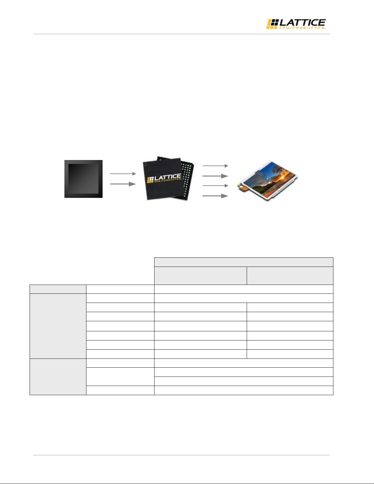
The Lattice Semiconductor MIPI®DSI to OpenLDI/FPD-Link/LVDS Interface Bridge IP with the Lattice Semiconductor
CrossLink™programmable device can translate DSI video streams from MIPI D-PHY interface to LVDS interface for an
FDP-Link connection to displays.
The Mobile Industry Processor Interface (MIPI) provides specifications for standardization in consumer mobile devices.
MIPI Display Serial Interface (DSI) and MIPI D-PHY specifications were developed to create a standardized interface for
all displays used in the mobile industry. As the industry evolves, bandwidth requirements have exceeded what display
manufacturers are capable of manufacturing, while application processor vendors can provide very fast interfacing
capabilities. For a cost effective solution, displays can be replaced with newer display, and the processor can be
retained. Low Voltage Differential Signaling (LVDS) interface has become popular to support fast data rates of video
transmission for Flat Panel Display Link (FPD-Link) connections.
Application
Processor
DCK
MIPI DSI LVDS
DCK0
D[0:3]
D0-D3 DCK1
D[4:7]
Figure 1.1. MIPI DSI to OpenLDI/FPD-Link/LVDS Interface Bridge System Diagram
1.1. Quick Facts
Table 1.1 provides quick facts about the MIPI DSI to OpenLDI/FPD-Link/LVDS Interface Bridge IP for CrossLink device.
Table 1.1. MIPI DSI to OpenLDI/FPD-Link/LVDS Interface Bridge IP Quick Facts
MIPI DSI to OpenLDI/FPD-Link/LVDS Interface Bridge IP Configuration
Single MIPI DSI to Single FPD-Link
(RX_GEAR=8, RGB888, HS_LP)
Dual MIPI DSI to Dual FPD-Link
(RX_GEAR=16, RGB888, HS_LP)
Core Requirements
FPGA Families Supported
CrossLink
Resource
Utilization
Targeted Device
LIF-MD6000-6MG81I
Data Path Width
32 bits total for 4 lanes
64 bits total for 4 lanes
LUTs
863
3367
sysMEM™EBRs
3
12
Registers
779
2636
Programmable IOs
22
22
Hard D-PHY
1
2
Design Tool
Support
Lattice Implementation
Lattice Diamond®3.8
Synthesis
Lattice Synthesis Engine
Synopsys®Synplify Pro®L-2016.03L
Simulation
Aldec®Active-HDL™10.3 Lattice Edition

MIPI DSI to OpenLDI/FPD-Link/LVDS Interface Bridge Soft IP
User Guide
© 2016 Lattice Semiconductor Corp. All Lattice trademarks, registered trademarks, patents, and disclaimers are as listed at www.latticesemi.com/legal. All other brand or product names are
trademarks or registered trademarks of their respective holders. The specifications and information herein are subject to change without notice.
FPGA-IPUG-02003-1.2 5
1.2. Features
The key features of the MIPI DSI to OpenLDI/FPD-Link/LVDS Interface Bridge IP are:
Compliant with MIPI D-PHY v1.1, MIPI DSI v1.1 and Open LVDS Display Interface (OpenLDI) v0.95 specifications
Supports MIPI DSI interfacing from 160 Mb/s up to 1.5 Gb/s
Supports 1:1, 1:2 (split) and 2:2 MIPI DSI to FPD-Link configurations
Supports 4 data lanes and one clock lane per MIPI DSI interface
Supports continuous and non-continuous MIPI D-PHY clock
Supports common MIPI DSI compatible video formats (RGB888, RGB666)
Supports MIPI DSI Video Mode operation of Non-Burst Mode with Sync Pulses
Supports dedicated EoT short packet (EoTp)
Transmits in OpenLDI unbalanced operating mode format
1.3. Conventions
1.3.1. Nomenclature
The nomenclature used in this document is based on Verilog HDL. This includes radix indications and logical operators.
1.3.2. Data Ordering and Data Types
The highest bit within a data bus is the most significant bit.
Single-bit data stream from each MIPI DSI data lane is deserialized into 8-bit or 16-bit parallel data where bit 0 is
the first received bit. The size of parallel data depends on the Rx gear setting (RX_GEAR).
Pixel data order before distribution to LVDS lanes is {Red[MSB:0], Green[MSB:0], Blue[MSB:0]}. One, two or four
pixels may be sent for distribution to LVDS lanes in one pixel clock cycle depending on number of Tx channels and
Tx gear setting (TX_GEAR). If there are multiple pixels per clock cycle, the pixel in the lower bits is the first received
pixel. For instance, the pixel order for 4 pixels per clock is {pixel3, pixel2, pixel1, pixel0} where pixel0 is received
first and pixel3 is received last.
Pixel data is transmitted over LVDS lanes according to OpenLDI 18-bit and 24-bit unbalanced operating mode
format.
1.3.3. Signal Names
Signal names that end with:
“_n” are active low
“_i” are input signals
Some signals are declared as bidirectional (IO) but are only used as input hence “_i” identifier is used.
“_o” are output signals
Some signals are declared as bidirectional (IO) but are only used as output hence “_o” identifier is used.

MIPI DSI to OpenLDI/FPD-Link/LVDS Interface Bridge Soft IP
User Guide
© 2016 Lattice Semiconductor Corp. All Lattice trademarks, registered trademarks, patents, and disclaimers are as listed at www.latticesemi.com/legal. All other brand or product names are
trademarks or registered trademarks of their respective holders. The specifications and information herein are subject to change without notice.
6 FPGA-IPUG-02003-1.2
2. Functional Description
The MIPI DSI to OpenLDI/FPD-Link/LVDS Interface Bridge IP serves as a bridge between a MIPI DSI host and a display
device.
2.1. Top
Figure 2.1 shows the MIPI DSI to OpenLDI/FPD-Link/LVDS Interface Bridge IP block diagram.
reset_n_i
clk_ref_i
clk_ch0_p_i
clk_ch0_n_i
d0_ch0_p_i
d0_ch0_n_i
d1_ch0_p_i
d1_ch0_n_i
d2_ch0_p_i
d2_ch0_n_i
d3_ch0_p_i
d3_ch0_n_i
clk_ch1_p_i
clk_ch1_n_i
d0_ch1_p_i
d0_ch1_n_i
d1_ch1_p_i
d1_ch1_n_i
d2_ch1_p_i
d2_ch1_n_i
d3_ch1_p_i
d3_ch1_n_i
clk_ch0_p_o
clk_ch0_n_o
d0_ch0_p_o
d0_ch0_n_o
d1_ch0_p_o
d1_ch0_n_o
d2_ch0_p_o
d2_ch0_n_o
d3_ch0_p_o
d3_ch0_n_o
clk_ch1_p_o
clk_ch1_n_o
d0_ch1_p_o
d0_ch1_n_o
d1_ch1_p_o
d1_ch1_n_o
d2_ch1_p_o
d2_ch1_n_o
d3_ch1_p_o
d3_ch1_n_o
lock_pll_o
pll_lol_o
ready_o
Figure 2.1. MIPI DSI to OpenLDI/FPD-Link/LVDS Interface Bridge IP Block Diagram
Table 2.1. MIPI DSI to OpenLDI/FPD-Link/LVDS Interface Bridge IP Pin Function Description
Port Name
Direction
Function Description
Clock and Reset
clk_ref_i
I
Reference clock for internal PLL. Available only when MIPI D-PHY clock is non-
continuous
reset_n_i
I
Asynchronous system reset (active low)
MIPI DSI Interface
clk_ch0_p_i, clk_ch0_n_i
IO
MIPI D-PHY channel 0 clock lane
d0_ch0_p_i, d0_ch0_n_i
IO
MIPI D-PHY channel 0 data lane 0
d1_ch0_p_i, d1_ch0_n_i
IO
MIPI D-PHY channel 0 data lane 1
d2_ ch0_p_i, d2_ ch0_n_i
IO
MIPI D-PHY channel 0 data lane 2
d3_ ch0_p_i, d3_ ch0_n_i
IO
MIPI D-PHY channel 0 data lane 3
clk_ch1_p_i, clk_ch1_n_i
IO
MIPI D-PHY channel 1 clock lane
d0_ch1_p_i, d0_ch1_n_i
IO
MIPI D-PHY channel 1 data lane 0. Available only for configurations with two Rx
channels

MIPI DSI to OpenLDI/FPD-Link/LVDS Interface Bridge Soft IP
User Guide
© 2016 Lattice Semiconductor Corp. All Lattice trademarks, registered trademarks, patents, and disclaimers are as listed at www.latticesemi.com/legal. All other brand or product names are
trademarks or registered trademarks of their respective holders. The specifications and information herein are subject to change without notice.
FPGA-IPUG-02003-1.2 7
Table 2.1. MIPI DSI to OpenLDI/FPD-Link/LVDS Interface Bridge IP Pin Function Description (Continued)
Port Name
Direction
Function description
d1_ch1_p_i, d1_ch1_n_i
IO
MIPI D-PHY channel 1 data lane 1. Available only for configurations with two Rx
channels
d2_ ch1_p_i, d2_ ch1_n_i
IO
MIPI D-PHY channel 1 data lane 2. Available only for configurations with two Rx
channels
d3_ ch1_p_i, d3_ ch1_n_i
IO
MIPI D-PHY channel 1 data lane 3. Available only for configurations with two Rx
channels
FPD-Link Interface
clk_ch0_p_o, clk_ch0_n_o
IO
LVDS channel 0 clock lane
d0_ch0_p_o, d0_ch0_n_o
IO
LVDS channel 0 data lane 0
d1_ch0_p_o, d1_ch0_n_o
IO
LVDS channel 0 data lane 1
d2_ ch0_p_o, d2_ ch0_n_o
IO
LVDS channel 0 data lane 2
d3_ ch0_p_o, d3_ ch0_n_o
IO
LVDS channel 0 data lane 3. Available only for configurations with RGB888 data
type
clk_ch1_p_o, clk_ch1_n_o
IO
LVDS channel 1 clock lane
d0_ch1_p_o, d0_ch1_n_o
IO
LVDS channel 1 data lane 0. Available only for configurations with two Tx
channels
d1_ch1_p_o, d1_ch1_n_o
IO
LVDS channel 1 data lane 1. Available only for configurations with two Tx
channels
d2_ ch1_p_o, d2_ ch1_n_o
IO
LVDS channel 1 data lane 2. Available only for configurations with two Tx
channels
d3_ ch1_p_o, d3_ ch1_n_o
IO
LVDS channel 1 data lane 3. Available only for configurations with two Tx
channels and RGB888 data type
Miscellaneous Status Signals
lock_pll_o
O
PLL lock (active high). Available only when miscellaneous status signals option
is enabled
pll_lol_o
O
PLL loss of lock (active high). Available only when miscellaneous status signals
option is enabled
ready_o
O
Indicates reset sequence of DDR components is complete (active high).
Available only when miscellaneous status signals option is enabled
Figure 2.2 shows the single MIPI DSI to OpenLDI/FPD-Link/LVDS Interface Bridge IP (1:1) block diagram.
DPHY Common Interface
Wrapper
Hard
DPHY
RX Global
Operations
Controller
LP HS
Controller
Capture
Controller
Byte2Pixel
FIFO
PLL
clk_ch0_p_i
clk_ch0_n_i
clk_byte_fr from DPHY
clk_pixel_i
vsync_o
hsync_o
de_o
Pixel data
clk_ref_i
or
clk_byte_fr from
DPHY
d0_ch0_p_i
d0_ch0_n_i
d1_ch0_p_i
d1_ch0_n_i
d2_ch0_p_i
d2_ch0_n_i
d3_ch0_p_i
d3_ch0_n_i
Lane Distr
p_odd_o
LVDS
Wrapper
clk_ch0_p_o
clk_ch0_n_o
d0_ch0_p_o
d0_ch0_n_o
d1_ch0_p_o
d1_ch0_n_o
d2_ch0_p_o
d2_ch0_n_o
d3_ch0_p_o
d3_ch0_n_o
OSC
clk_lp_ctrl
eclk
clk_ref_i
or
clk_byte_fr from
DPHY
clk_ref_i
or
clk_byte_fr from
DPHY
Figure 2.2. Single MIPI DSI to OpenLDI/FPD-Link/LVDS Interface Bridge IP (1:1) Block Diagram

MIPI DSI to OpenLDI/FPD-Link/LVDS Interface Bridge Soft IP
User Guide
© 2016 Lattice Semiconductor Corp. All Lattice trademarks, registered trademarks, patents, and disclaimers are as listed at www.latticesemi.com/legal. All other brand or product names are
trademarks or registered trademarks of their respective holders. The specifications and information herein are subject to change without notice.
8 FPGA-IPUG-02003-1.2
Figure 2.3 shows the MIPI DSI to OpenLDI/FPD-Link/LVDS Interface Bridge IP (1:2, Split) block diagram.
DPHY Common Interface
Wrapper
Hard
DPHY
RX Global
Operations
Controller
LP HS
Controller
Capture
Controller
Byte2Pixel
FIFO
PLL
clk_byte_fr from DPHY
clk_pixel_i
clk_byte_fr
from PLL
vsync_o
hsync_o
de_o
Pixel data
clk_ref_i
or
clk_byte_fr from
DPHY
Lane Distr
p_odd_o
LVDS
Wrapper
clk_ch0_p_o
clk_ch0_n_o
d0_ch0_p_o
d0_ch0_n_o
d1_ch0_p_o
d1_ch0_n_o
d2_ch0_p_o
d2_ch0_n_o
d3_ch0_p_o
d3_ch0_n_o
OSC
clk_lp_ctrl
eclk
clk_ch0_p_i
clk_ch0_n_i
d0_ch0_p_i
d0_ch0_n_i
d1_ch0_p_i
d1_ch0_n_i
d2_ch0_p_i
d2_ch0_n_i
d3_ch0_p_i
d3_ch0_n_i
clk_ref_i
or
clk_byte_fr from
DPHY
clk_ref_i
or
clk_byte_fr from
DPHY
clk_ch1_p_o
clk_ch1_n_o
d0_ch1_p_o
d0_ch1_n_o
d1_ch1_p_o
d1_ch1_n_o
d2_ch1_p_o
d2_ch1_n_o
d3_ch1_p_o
d3_ch1_n_o
Figure 2.3. MIPI DSI to OpenLDI/FPD-Link/LVDS Interface Bridge IP (1:2, Split) Block Diagram
Figure 2.4 shows the MIPI DSI to OpenLDI/FPD-Link/LVDS Interface Bridge IP (2:2) block diagram.
DPHY Common Interface
Wrapper
Hard
DPHY
RX Global
Operations
Controller
LP HS
Controller
Capture
Controller
Byte2Pixel
FIFO
PLL
clk_ch0_p_i
clk_ch0_n_i
clk_byte_fr from DPHY
clk_pixel_i
(channel 0)
vsync_o
hsync_o
de_o
Pixel data
clk_ref_i
or
clk_byte_fr from
DPHY channel 0
d0_ch0_p_i
d0_ch0_n_i
d1_ch0_p_i
d1_ch0_n_i
d2_ch0_p_i
d2_ch0_n_i
d3_ch0_p_i
d3_ch0_n_i
Lane Distr
p_odd_o
LVDS
Wrapper
clk_ch0_p_o
clk_ch0_n_o
d0_ch0_p_o
d0_ch0_n_o
d1_ch0_p_o
d1_ch0_n_o
d2_ch0_p_o
d2_ch0_n_o
d3_ch0_p_o
d3_ch0_n_o
OSC
clk_lp_ctrl
eclk
DPHY Common Interface
Wrapper
Hard
DPHY
Capture
Controller
Byte2Pixel
FIFO
clk_ch1_p_i
clk_ch1_n_i
vsync_o
hsync_o
de_o
Pixel data
d0_ch1_p_i
d0_ch1_n_i
d1_ch1_p_i
d1_ch1_n_i
d2_ch1_p_i
d2_ch1_n_i
d3_ch1_p_i
d3_ch1_n_i
Lane Distr
p_odd_o
LVDS
Wrapper
clk_ch1_p_o
clk_ch1_n_o
d0_ch1_p_o
d0_ch1_n_o
d1_ch1_p_o
d1_ch1_n_o
d2_ch1_p_o
d2_ch1_n_o
d3_ch1_p_o
d3_ch1_n_o
clk_byte_fr clk_byte_fr
clk_pixel_i
(channel 1)
clk_ref_i
or
clk_byte_fr from
DPHY channel 0
clk_ref_i
or
clk_byte_fr from
DPHY channel 0
Figure 2.4. MIPI DSI to OpenLDI/FPD-Link/LVDS Interface Bridge IP (2:2) Block Diagram
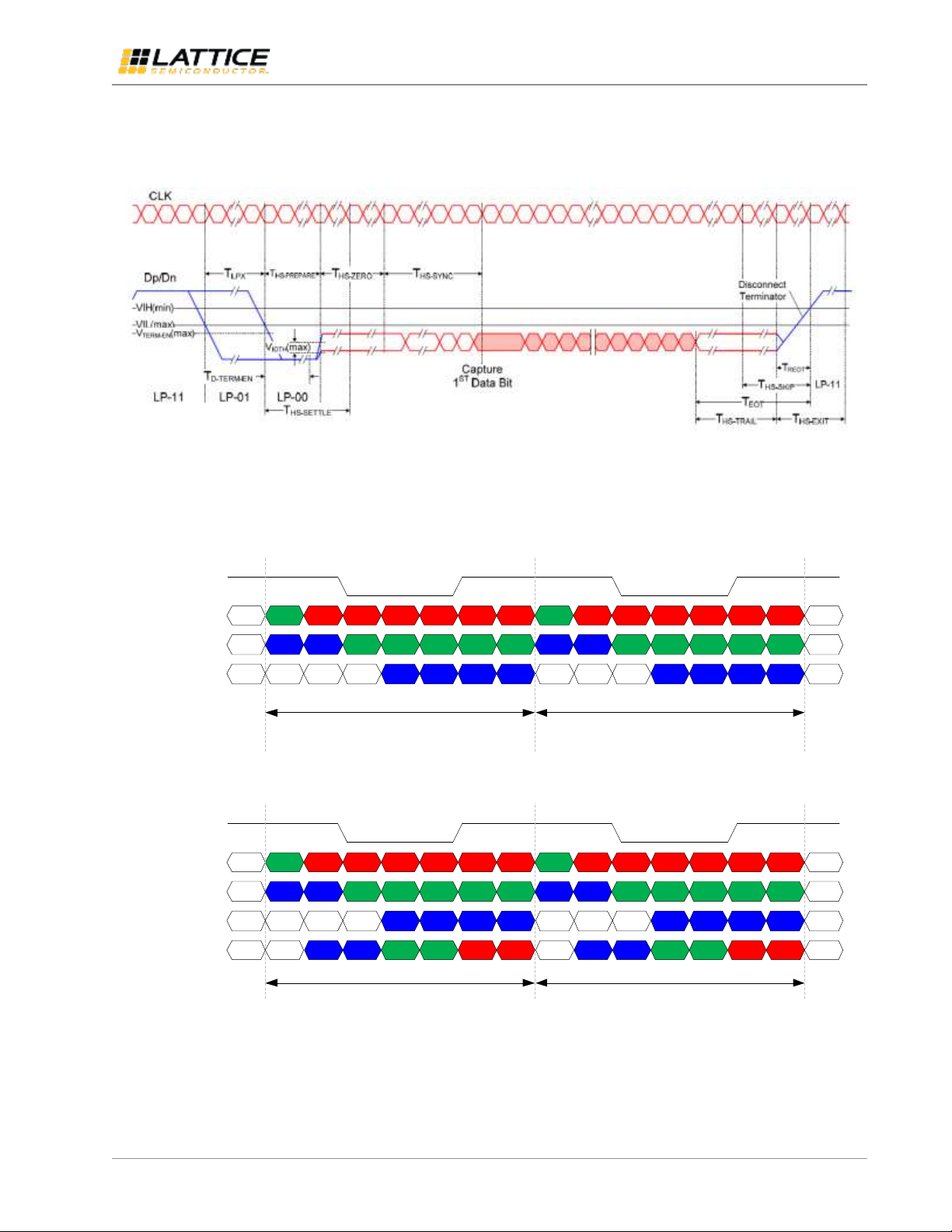
The MIPI DSI receive interface has one MIPI D-PHY clock lane and four MIPI D-PHY data lanes. The clock lane is center-
aligned to the data lanes. The clock lane can either be continuous (high speed only, HS_ONLY) or non-continuous
(HS_LP).
When the clock lane is non-continuous, proper transition from low power (LP) to high speed (HS) mode of clock lane is
required. The data lanes also require proper transition from LP to HS modes. In HS mode, data stream from each data
MIPI DSI to OpenLDI/FPD-Link/LVDS Interface Bridge Soft IP
User Guide
© 2016 Lattice Semiconductor Corp. All Lattice trademarks, registered trademarks, patents, and disclaimers are as listed at www.latticesemi.com/legal. All other brand or product names are
trademarks or registered trademarks of their respective holders. The specifications and information herein are subject to change without notice.
FPGA-IPUG-02003-1.2 9
lane is deserialized to byte data. The deserialization is done with 1:8 gearing or 1:16 gearing depending on Rx gear
setting (RX_GEAR). The byte data is word-aligned based on the SoT Sync sequence defined in the MIPI D-PHY
Specification version 1.1.
Figure 2.5. High-Speed Data Transmission
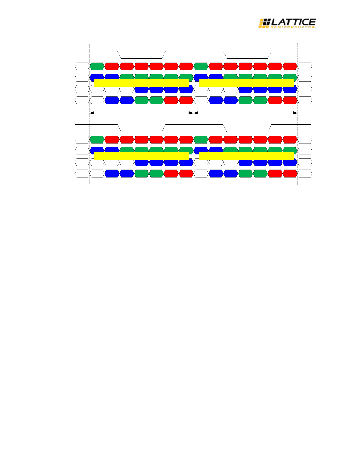
RGB data and control signals extracted from DSI packets are transmitted over FPD-Link interface such that output is
compliant to OpenLDI unbalanced format as shown in Figure 2.6 –Figure 2.8. Control signals include data enable (DE),
vertical and horizontal sync flags (VSYNC and HSYNC). Reserved bits (RES) are tied to 0.
VSYNC HSYNCDE VSYNC HSYNCDE
R0
G1
B2
R1
G2
B3
R2
G3
B4
R3
G4
B5
R4
G5
R5
B0
G0
B1
R0
G1
B2
R1
G2
B3
R2
G3
B4
R3
G4
B5
R4
G5
R5
B0
G0
B1
Current Cycle Next Cycle
clk_ch0_p_o
d0_ch0_p_o
d1_ch0_p_o
d2_ch0_p_o
Figure 2.6. FPD-Link Transmit Interface Timing Diagram (RGB666)
VSYNC HSYNCDE VSYNC HSYNCDE
R0
G1
B2
R1
G2
B3
R2
G3
B4
R3
G4
B5
R4
G5
R5
B0
G0
B1
R0
G1
B2
R1
G2
B3
R2
G3
B4
R3
G4
B5
R4
G5
R5
B0
G0
B1
Current Cycle Next Cycle
RES RESR6R7G6G7B6B7 R6R7G6G7B6B7
clk_ch0_p_o
d0_ch0_p_o
d1_ch0_p_o
d2_ch0_p_o
d3_ch0_p_o
Figure 2.7. FPD-Link Transmit Interface Timing Diagram (RGB888)
MIPI DSI to OpenLDI/FPD-Link/LVDS Interface Bridge Soft IP
User Guide
© 2016 Lattice Semiconductor Corp. All Lattice trademarks, registered trademarks, patents, and disclaimers are as listed at www.latticesemi.com/legal. All other brand or product names are
trademarks or registered trademarks of their respective holders. The specifications and information herein are subject to change without notice.
10 FPGA-IPUG-02003-1.2
VSYNC HSYNCDE VSYNC HSYNCDE
R0
G1
B2
R1
G2
B3
R2
G3
B4
R3
G4
B5
R4
G5
R5
B0
G0
B1
R0
G1
B2
R1
G2
B3
R2
G3
B4
R3
G4
B5
R4
G5
R5
B0
G0
B1
Current Cycle Next Cycle
RES RESR6R7G6G7B6B7 R6R7G6G7B6B7
clk_ch0_p_o
d0_ch0_p_o
d1_ch0_p_o
d2_ch0_p_o
d3_ch0_p_o
VSYNC HSYNCDE VSYNC HSYNCDE
R0
G1
B2
R1
G2
B3
R2
G3
B4
R3
G4
B5
R4
G5
R5
B0
G0
B1
R0
G1
B2
R1
G2
B3
R2
G3
B4
R3
G4
B5
R4
G5
R5
B0
G0
B1
RES RESR6R7G6G7B6B7 R6R7G6G7B6B7
clk_ch1_p_o
d0_ch1_p_o
d1_ch1_p_o
d2_ch1_p_o
d3_ch1_p_o
1st pixel received
2nd pixel received
3rd pixel received
4th pixel received
Figure 2.8. Single MIPI DSI to Dual FPD-Link (Split) Timing Diagram
Each data lane is serialized using ODDRx7 or ODDRx14 primitive, depending on Tx gear setting (TX_GEAR). RGB888
requires 4 data lanes while RGB666 requires 3 data lanes only. The clock lane is generated by feeding constant
“1100011” or “11000111100011” to another ODDRx7 or ODDRx14, respectively. The clock is edge-aligned against data.
Seven bits of data are transmitted in one clock cycle. When TX_GEAR is 14, the first pixel received is transmitted first
and the second pixel received is transmitted in the next clock cycle.
In single MIPI DSI to dual FPD-Link configuration, the incoming packets are split into the two channels in an alternate
manner. The first pixel received is transmitted over LVDS channel 0 while the next pixel received is transmitted over
LVDS channel 1 at the same clock cycle as shown in Figure 2.8. The same approach is implemented regardless of
TX_GEAR setting.
The dual MIPI DSI to dual FPD-Link configuration is two instances of single MIPI DSI to single FPD-Link that share the
same clocks. When MIPI D-PHY clock is continuous, the continuous byte clock from Rx channel 0 is used.
2.2. D-PHY Common Interface Wrapper
When two Rx channels are enabled, each channel has its own D-PHY common interface wrapper. This block instantiates
and configures hard D-PHY IP to receive MIPI D-PHY high-speed data from all enabled data lanes. The hard D-PHY IP
outputs 8-bit or 16-bit parallel data in non-continuous byte clock domain for each data lane. Size of parallel data
depends on Rx gear setting (RX_GEAR).
Byte data are transferred to continuous byte clock domain using multicycle registers. Data enable signal from this block
becomes active when SoT Sync is successfully detected by hard D-PHY IP from all enabled data lanes and becomes
inactive when MIPI D-PHY data lanes go to Stop state (LP11).
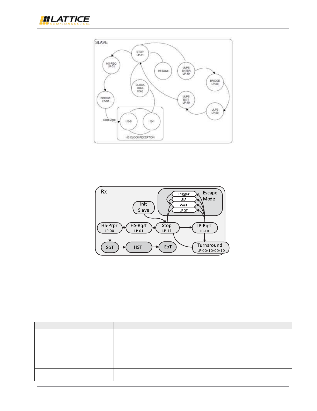
2.3. Rx Global Operations Controller
When two Rx channels are enabled, each channel has its own Rx global operations controller. This block controls the
high-speed termination enable of MIPI D-PHY clock and data lanes. When MIPI D-PHY clock is continuous, the HS
termination enable of clock lane is tied to VCC. When MIPI D-PHY clock is non-continuous, the HS termination enable of
clock lane becomes active after proper LP to HS transition is observed. Oscillator clock is used for this function. The
required LP to HS transition on clock lane is shown in Figure 2.9 as per MIPI D-PHY Specification version 1.1.
MIPI DSI to OpenLDI/FPD-Link/LVDS Interface Bridge Soft IP
User Guide
© 2016 Lattice Semiconductor Corp. All Lattice trademarks, registered trademarks, patents, and disclaimers are as listed at www.latticesemi.com/legal. All other brand or product names are
trademarks or registered trademarks of their respective holders. The specifications and information herein are subject to change without notice.
FPGA-IPUG-02003-1.2 11
Figure 2.9. MIPI D-PHY Clock Lane Module State Diagram
Similarly, HS termination enable of data lanes becomes high after proper LP to HS transition is detected on data lane 0.
A free-running byte clock is used for this function. The required LP to HS transition on data lanes is shown in Figure 2.10
as per MIPI D-PHY Specification version 1.1.
Figure 2.10. MIPI D-PHY Data Lane Module State Diagram
2.4. Capture Controller
When two Rx channels are enabled, each channel has its own capture controller. This block takes data bytes from
D-PHY Common Interface Wrapper and detects short and long packets defined by MIPI DSI to generate sync signals and
extract video data and other control parameters. Table 2.2 shows outputs of this block that are relevant to MIPI DSI to
OpenLDI/FPD-Link/LVDS Interface Bridge IP.
Table 2.2. Capture Controller Outputs
Port Name
Direction
Function Description
payload_en_o
Output
Payload data enable to indicate when byte to pixel conversion is required (active high)
payload_o[MSB:0]
Output
Video data or payload. Data width is Rx lanes * RX_GEAR
sp_en_o
Output
Short packet enable. Goes high for 1 byte clock cycle when short packet is detected (active
high)
sp2_en_o
Output
Short packet enable. Goes high for 1 byte clock cycle when short packet is detected from
the higher byte when RX_GEAR=16 (active high)
lp_en_o
Output
Long packet enable. Goes high for 1 byte clock cycle when long packet is detected (active
high)
MIPI DSI to OpenLDI/FPD-Link/LVDS Interface Bridge Soft IP
User Guide
© 2016 Lattice Semiconductor Corp. All Lattice trademarks, registered trademarks, patents, and disclaimers are as listed at www.latticesemi.com/legal. All other brand or product names are
trademarks or registered trademarks of their respective holders. The specifications and information herein are subject to change without notice.
12 FPGA-IPUG-02003-1.2
Table 2.2. Capture Controller Outputs (Continued)
Port Name
Direction
Function description
lp2_en_o
Output
Long packet enable. Goes high for 1 byte clock cycle when long packet is detected from the
higher byte when RX_GEAR=16 (active high)
lp_av_en_o
Output
Long packet enable for active video data. Goes high for 1 byte clock cycle when long
packet containing active video is detected (active high)
lp2_av_en_o
Output
Long packet enable for active video data. Goes high for 1 byte clock cycle when long
packet containing active video is detected from the higher byte when RX_GEAR=16 (active
high)
vc_o[1:0]
Output
Virtual channel
vc2_o[1:0]
Output
Virtual channel from higher byte when RX_GEAR=16
wc_o[15:0]
Output
Word count of long packet
wc2_o[15:0]
Output
Word count of long packet from higher byte when RX_GEAR=16
dt_o[5:0]
Output
Data type
dt2_o[5:0]
Output
Data type from higher byte when RX_GEAR=16
ecc_o[7:0]
Output
ECC of packet header
ecc2_o[7:0]
Output
ECC of packet header from higher byte when RX_GEAR=16
2.5. Byte2Pixel
When two Rx channels are enabled, each channel has its own byte2pixel. This block converts byte data into pixel data
using FIFO. Continuous byte clock is used to write data to FIFO while pixel clock is used to read data from FIFO.
The VSYNC and HSYNC outputs are also generated by this block and transferred to pixel clock domain using
synchronization registers. Since only DSI Non-Burst Mode with Sync Pulses is supported, the generation of VSYNC and
HSYNC control signals is dependent on the MIPI DSI host device as follows. VSYNC goes active high and inactive low
when the “VSYNC Start” and “VSYNC End” short packets are seen, respectively. HSYNC goes active high when the
“HSYNC Start”, “VSYNC Start” and “VSYNC End” short packets are seen. HSYNC goes inactive low when the “HSYNC
end” short packet is seen. MIPI DSI Non-Burst Mode with Sync Events and Burst Mode operations are not supported.
2.6. Lane Distribution
When two Rx channels are enabled, each channel has its own lane distribution. This block is the interface between
byte2pixel and lvds wrapper. It rearranges pixel data bits according to OpenLDI unbalanced format discussed in the Top
section on page 6. The arranged data bits are fed to lvds wrapper for transmission over LVDS lanes.
When TX_GEAR=14 and/or two Tx channels are enabled, multiple pixels are received from byte2pixel in one pixel clock
cycle. There may be cases when not all of the pixels received in one cycle are valid, for example odd number of pixels.
This module uses p_odd_o output of byte2pixel to determine which of the pixels are valid.
2.7. LVDS Wrapper
This block instantiates one ODDRx7 or one ODDRx14 primitive to serialize parallel data for each LVDS data lane.
Selection between ODDRx7 and ODDRx14 depends on Tx gear setting. The clock lane is generated by feeding constant
“1100011” or “11000111100011” to another ODDRx7 or ODDRx14, respectively.
This block also divides PLL output clock to generate pixel clock.
A reset synchronization module is enclosed within this block. It takes care of the reset sequence of ODDR blocks and
other DDR primitives. Start of HS transmission should only begin when reset synchronization sequence is complete.
This block drives its output ready_o high when reset synchronization sequence is complete.
MIPI DSI to OpenLDI/FPD-Link/LVDS Interface Bridge Soft IP
User Guide
© 2016 Lattice Semiconductor Corp. All Lattice trademarks, registered trademarks, patents, and disclaimers are as listed at www.latticesemi.com/legal. All other brand or product names are
trademarks or registered trademarks of their respective holders. The specifications and information herein are subject to change without notice.
FPGA-IPUG-02003-1.2 13
2.8. Reset and Clocking
Asynchronous active low reset input (reset_n_i) is used as a system reset. Local reset signals are derived from the
system reset to create asynchronous reset assertion and synchronous reset deassertion for logic in different clock
domains (non-continuous byte clock not included). Logic in continuous byte clock and pixel clock domains are also reset
when ready_o from lvds_wrapper is low. Logic in LVDS wrapper is reset when PLL lock is low. The system reset input
must be asserted for at least 60 ns.
Internal PLL could take ~15 ms to be locked after PLL reference clock is made available. Data loss is expected when
incoming MIPI DSI transaction begins during this period when PLL lock is not yet obtained. To avoid malfunction, the
MIPI DSI to OpenLDI/FPD-Link/LVDS Interface Bridge IP discards any received MIPI DSI packets until it detects “VSYNC
start” short packet.
When MIPI D-PHY clock is continuous, it is expected to be in high speed mode at power on of the device. The HS
termination enable of clock lane is tied to VCC. Continuous byte clock is generated by hard D-PHY IP and used as PLL
reference clock. Internal PLL generates eclk used to serialize data. A clock divider is used to generate pixel clock inside
the lvds wrapper.
When MIPI D-PHY clock is non-continuous, an external clock source (clk_ref_i) is needed for PLL reference clock.
Internal PLL generates continuous byte clock and eclk. Internal oscillator clock is used to detect LP to HS transition of
clock lane and for reset synchronization sequence of DDR components inside lvds wrapper. Internal oscillator
generates ~48 MHz clock.
Maximum fabric clock of CrossLink device is 150 MHz while maximum continuous byte clock is 112.5 MHz due to heavy
logic inside capture controller and byte2pixel core modules. Rx gear 16 and Tx gear 14 features are added to achieve
higher data rates by doubling the parallel data bus width and dividing byte clock and pixel clock by 2, respectively.
For single Rx to single Tx and dual Rx to dual Tx configurations, the Rx line rate is limited by maximum Tx line rate that
is 1.2 Gb/s.
Frequency calculations are given in Table 2.3. DCK refers to MIPI D-PHY clock frequency.
Table 2.3. Clock Frequency Calculations
Clock
Formula
Rx line rate
DCK * 2
Tx line rate
LVDS Output clock * 7
D-PHY clock
DCK
Byte clock
DCK / (RX_GEAR/2)
Pixel clock
Byte clock * Rx lanes * RX_GEAR / (Pixel width * Pixels per pixel clock cycle) , where pixels per pixel clock
cycle is:
TX_GEAR/7 –for single Rx to single Tx or dual Rx to dual Tx
TX_GEAR/3.5 –for single Rx to dual Tx
eclk
Pixel clock * (TX_GEAR/2)
LVDS output clock
Pixel clock * (TX_GEAR/7)
Reference clock
Byte clock

MIPI DSI to OpenLDI/FPD-Link/LVDS Interface Bridge Soft IP
User Guide
© 2016 Lattice Semiconductor Corp. All Lattice trademarks, registered trademarks, patents, and disclaimers are as listed at www.latticesemi.com/legal. All other brand or product names are
trademarks or registered trademarks of their respective holders. The specifications and information herein are subject to change without notice.
14 FPGA-IPUG-02003-1.2
Table 2.4. Supported Data Rates for MIPI DSI to OpenLDI/FPD-Link/LVDS Interface Bridge IP Configurations
Configuration
D-PHY line rate
(Mb/s)
DCK
(MHz)
Data Type
RX_GEAR
TX_GEAR
Single DSI to Single FPD-Link
RGB666
8
7
160 –675
40 –337.5
14
675 –771.42
337.5 –385.74
RGB888 /
RGB666_LOOSE
8
7
160 –900
40 –450
16
14
900 –1028.57
450 –514.28
Single DSI to Dual FPD-Link
RGB666
8
7
160 –900
40 –450
16
14
900 –1500
450 –750
RGB888 /
RGB666_LOOSE
8
7
160 –900
40 –450
16
14
900 –1500
450 –750
Dual DSI to Dual FPD-Link
Same as Single DSI to Single FPD-Link

MIPI DSI to OpenLDI/FPD-Link/LVDS Interface Bridge Soft IP
User Guide
© 2016 Lattice Semiconductor Corp. All Lattice trademarks, registered trademarks, patents, and disclaimers are as listed at www.latticesemi.com/legal. All other brand or product names are
trademarks or registered trademarks of their respective holders. The specifications and information herein are subject to change without notice.
FPGA-IPUG-02003-1.2 15
3. Parameter Settings
Table 3.1 shows the parameters used to generate MIPI DSI to OpenLDI/FPD-Link/LVDS Interface Bridge IP.
Table 3.1. MIPI DSI to OpenLDI/FPD-Link/LVDS Interface Bridge IP Parameter Settings
Parameter
Attribute
Options
Description
Number of Rx channels
User-input
1 or 2
Number of MIPI D-PHY channels.
If 2 is selected, the following Rx settings will be applied
to both Rx channels
Rx Interface
Fixed
MIPI DSI
Receive interface
Number of Rx lanes
Fixed
4
Number of MIPI D-PHY data lanes
Rx gearing
Read-only
8 or 16
Gearbox ratio of receive interface, automatically
selected based on Rx data rate (see Reset and Clocking
section on page 13)
Rx D-PHY IP
Fixed
Hard D-PHY
MIPI D-PHY Implementation
Number of Tx channels
User-input
1 or 2
Number of LVDS channels
Tx Interface
Fixed
LVDS
Transmit interface (FPD-Link)
Number of Tx lanes
Read-only
3 or 4
Derived from data type: 3 lanes for RGB666 while 4
lanes for RGB888
Tx gearing
Read-only
7 or 14
Gearbox ratio of transmit interface, automatically
selected based on Rx data rate (see Reset and Clocking
section on page 13)
Rx Line Rate
User-input
See Table 2.4
Data rate per MIPI D-PHY lane
Tx Line Rate
Read-only
See Table 2.3
Data rate per LVDS lane
D-PHY Clock Frequency
Read-only
See Table 2.3
MIPI D-PHY clock frequency (DCK).
tHS-SETTLE MIPI D-PHY timing parameter is also derived
from this setting (85 ns + 6 UI).
tHS-SETTLE counter is implemented in byte clock domain.
The expected actual tHS-SETTLE is ~2 byte clock cycles
more than the computed value.
D-PHY Clock Mode
User-input
Continuous or Non-
continuous
MIPI D-PHY clock mode
Byte Clock Frequency
Read-only
See Table 2.3
Byte clock frequency
Pixel Clock Frequency
Read-only
See Table 2.3
Pixel clock frequency
Eclk Frequency
Read-only
See Table 2.3
Serializer clock frequency
LVDS Clock Frequency
Read-only
See Table 2.3
LVDS clock frequency
Reference Clock Frequency
Read-only
See Table 2.3
Reference clock frequency
Miscellaneous Signals
User-input
Marked or Unmarked
Brings out miscellaneous status signals to port
Data Type
User-input
RGB888 or RGB666
Supported MIPI DSI data types
RGB666 Type
User-input
Packed or Loosely
Packed
Selects between RGB666 Packed and Loosely Packed
formats
MIPI DSI to OpenLDI/FPD-Link/LVDS Interface Bridge Soft IP
User Guide
© 2016 Lattice Semiconductor Corp. All Lattice trademarks, registered trademarks, patents, and disclaimers are as listed at www.latticesemi.com/legal. All other brand or product names are
trademarks or registered trademarks of their respective holders. The specifications and information herein are subject to change without notice.
16 FPGA-IPUG-02003-1.2
4. IP Generation and Evaluation
This section provides information on how to generate MIPI DSI to OpenLDI/FPD-Link/LVDS Interface Bridge IP using the
Diamond Clarity Designer, and how to run simulation, synthesis and hardware evaluation.
4.1. Licensing the IP
An IP-specific license is required to enable full, unrestricted use of the MIPI DSI to OpenLDI/FPD-Link/LVDS Interface
Bridge IP in a complete, top-level design. The MIPI DSI to OpenLDI/FPD-Link/LVDS Interface Bridge IP is available free of
charge.
Please request your free license by sending an email to lic_ad[email protected] attaching your existing Lattice
Diamond license or providing your MacID along with the IP details.
You may download or generate the MIPI DSI to OpenLDI/FPD-Link/LVDS Interface Bridge IP and fully evaluate it
through functional simulation and implementation (synthesis, map, place and route) without the IP license. The MIPI
DSI to OpenLDI/FPD-Link/LVDS Interface Bridge IP also supports Lattice’s IP hardware evaluation capability, which
makes it possible to create versions of the IP that operate in hardware for a limited time (approximately four hours)
without requiring an IP license. See the Hardware Evaluation section on page 25 for further details. However, the IP
license is required to enable timing simulation, to open the design in Diamond EPIC tool, or to generate bitstreams that
do not include the hardware evaluation timeout limitation.
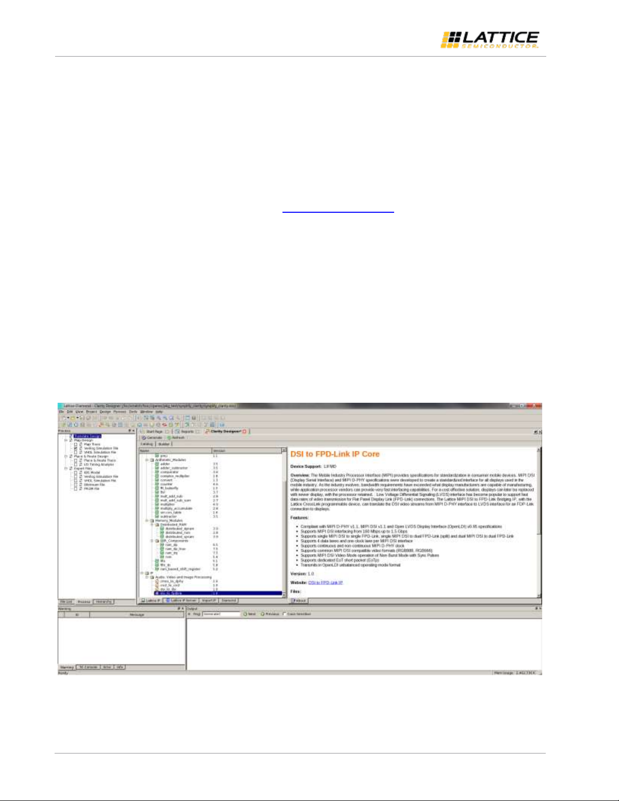
4.2. Getting Started
The MIPI DSI to OpenLDI/FPD-Link/LVDS Interface Bridge IP is available for download from the Lattice IP Server using
the Clarity Designer tool. The IP files are automatically installed using ispUPDATE technology in any customer-specified
directory. After the IP has been installed, the IP is available in the Clarity Design GUI as shown in Figure 4.1.
Figure 4.1. Clarity Designer Window
MIPI DSI to OpenLDI/FPD-Link/LVDS Interface Bridge Soft IP
User Guide
© 2016 Lattice Semiconductor Corp. All Lattice trademarks, registered trademarks, patents, and disclaimers are as listed at www.latticesemi.com/legal. All other brand or product names are
trademarks or registered trademarks of their respective holders. The specifications and information herein are subject to change without notice.
FPGA-IPUG-02003-1.2 17
4.3. Generating IP in Clarity Designer
The Clarity Designer tool is used to customize modules and IPs and place them into the device’s architecture.
The following describes the procedure for generating MIPI DSI to OpenLDI/FPD-Link/LVDS Interface Bridge IP in Clarity
Designer.
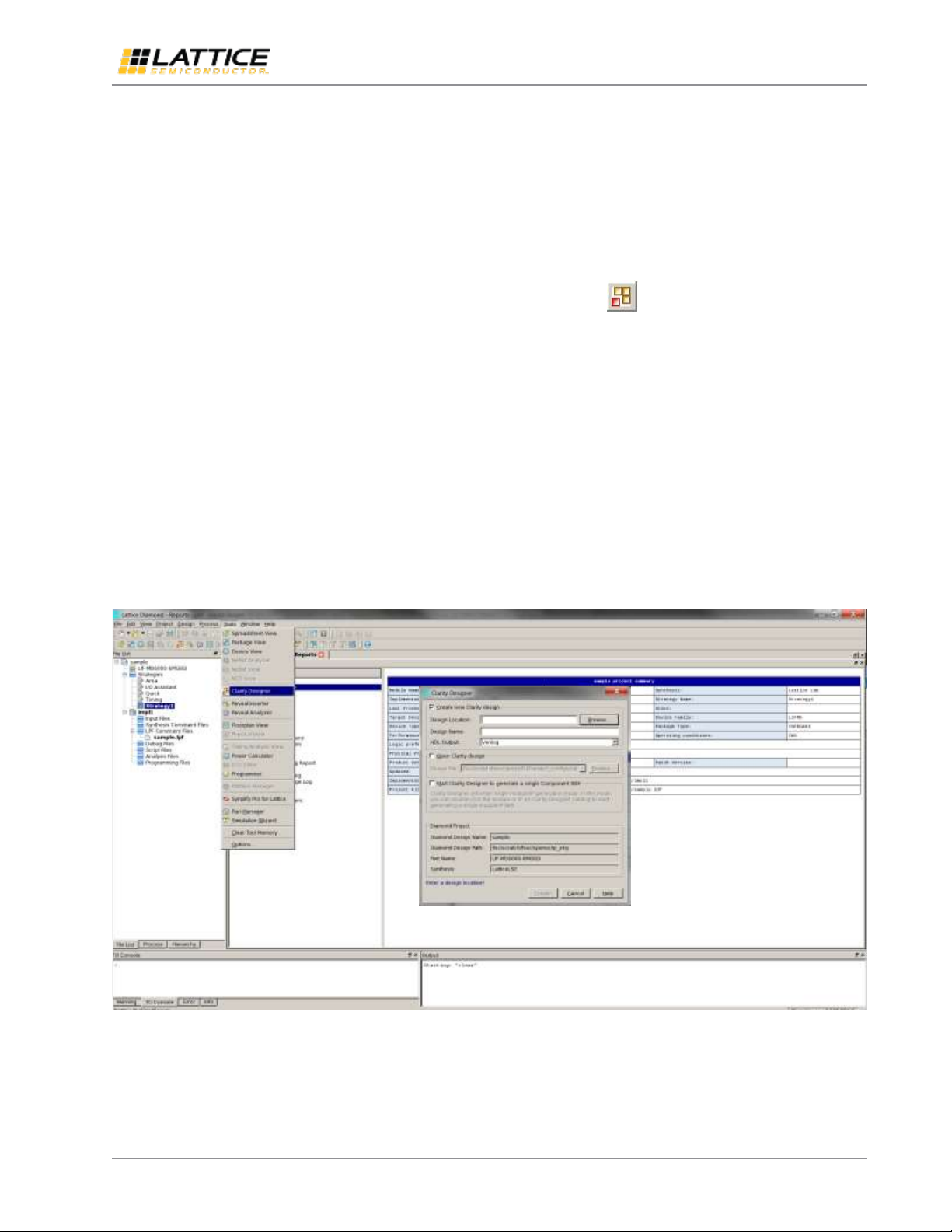
Clarity Designer can be started from the Diamond design environment.
To start Clarity Designer:
1. Create a new empty Diamond project for CrossLink family devices.
2. From the Diamond main window, choose Tools > Clarity Designer, or click in Diamond toolbox. The Clarity
Designer project dialog box is displayed.
3. Select and fill out the following items as shown in Figure 4.2:
Create new Clarity design –Choose to create a new Clarity Design project directory in which the MIPI DSI to
OpenLDI/FPD-Link/LVDS Interface Bridge IP will be generated.
Design Location –Clarity Design project directory path.
Design Name –Clarity Design project name.
HDL Output –Hardware Description Language Output Format (Verilog).
The Clarity Designer project dialog box also allows you to open an existing Clarity Designer project by selecting the
following:
Open Clarity design –Open an existing Clarity Design project.
Design File –Name of existing Clarity Design project file with .sbx extension.
4. Click the Create button. A new Clarity Designer project is created.
Figure 4.2. Starting Clarity Designer from Diamond Design Environment
To configure the MIPI DSI to OpenLDI/FPD-Link/LVDS Interface Bridge IP in Clarity Designer:
1. Double-click dsi_to_fpdlink in the IP list of the Catalog view. The dsi_to_fpdlink dialog box is displayed as shown in
Figure 4.3.

MIPI DSI to OpenLDI/FPD-Link/LVDS Interface Bridge Soft IP
User Guide
© 2016 Lattice Semiconductor Corp. All Lattice trademarks, registered trademarks, patents, and disclaimers are as listed at www.latticesemi.com/legal. All other brand or product names are
trademarks or registered trademarks of their respective holders. The specifications and information herein are subject to change without notice.
18 FPGA-IPUG-02003-1.2
Figure 4.3. Configuring MIPI DSI to OpenLDI/FPD-Link/LVDS Interface Bridge IP in Clarity Designer
2. Enter the Instance Name.
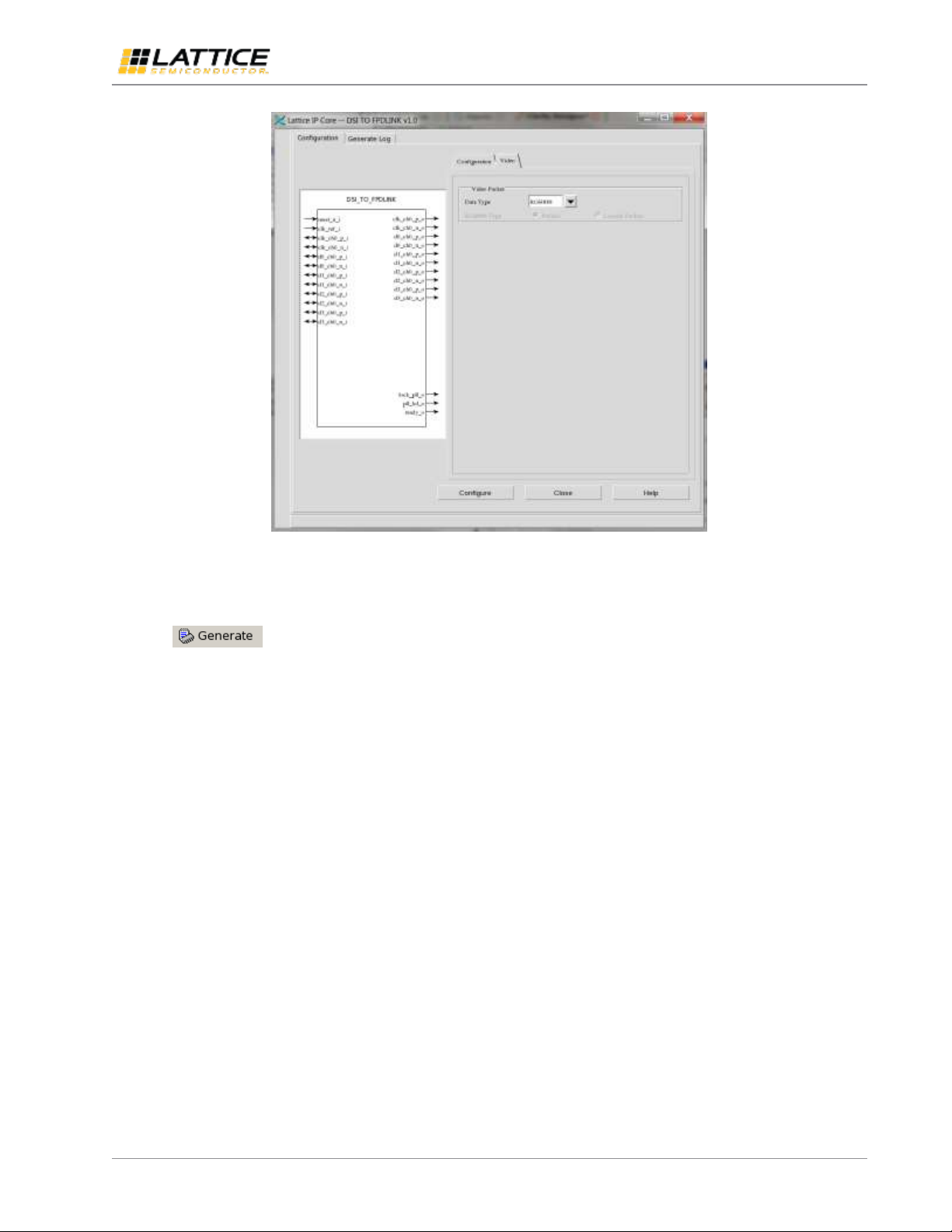
3. Click the Customize button. An IP configuration interface is displayed as shown in Figure 4.4 and Figure 4.5. From
this dialog box, you can select the IP parameter options specific to your application. The parameters are grouped
into two tabs: Configuration and Video.
Figure 4.4. Configuration Tab in IP GUI
MIPI DSI to OpenLDI/FPD-Link/LVDS Interface Bridge Soft IP
User Guide
© 2016 Lattice Semiconductor Corp. All Lattice trademarks, registered trademarks, patents, and disclaimers are as listed at www.latticesemi.com/legal. All other brand or product names are
trademarks or registered trademarks of their respective holders. The specifications and information herein are subject to change without notice.
FPGA-IPUG-02003-1.2 19
Figure 4.5. Video Tab in IP GUI
4. Select the required parameters, and click the Configure button.
5. Click Close.
6. Click in the toolbox. Clarity Designer generates all the IPs and modules, and creates a top module to
wrap them.
For detailed instructions on how to use the Clarity Designer, refer to the Lattice Diamond software user guide.
MIPI DSI to OpenLDI/FPD-Link/LVDS Interface Bridge Soft IP
User Guide
© 2016 Lattice Semiconductor Corp. All Lattice trademarks, registered trademarks, patents, and disclaimers are as listed at www.latticesemi.com/legal. All other brand or product names are
trademarks or registered trademarks of their respective holders. The specifications and information herein are subject to change without notice.
20 FPGA-IPUG-02003-1.2
4.4. Generated IP Directory Structure and Files
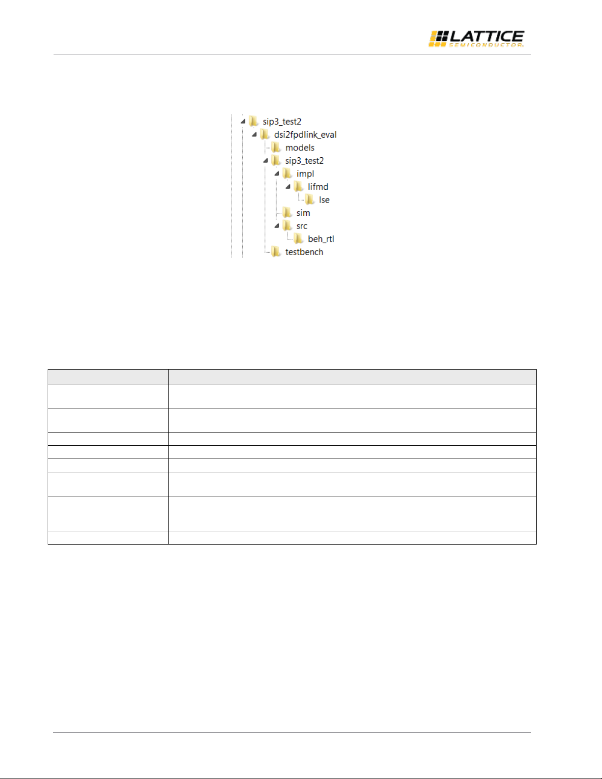
The directory structure of generated IP files is shown in Figure 4.6.
Figure 4.6. IP Directory Structure
The design flow for the IP created with Clarity Designer uses post-synthesized modules (NGO) of the IP core modules
for synthesis and uses protected models for simulation. The post-synthesized modules are customized when you
configure the IP and created automatically when the IP is generated. The protected models are common to all
configurations.
Table 4.1 provides a list of key files and directories created by Clarity Designer with details on how they are used.
Table 4.1. Files Generated by Clarity Designer
File
Description
<instance_name>.v
Verilog top-level module of MIPI DSI to OpenLDI/FPD-Link/LVDS Interface Bridge IP used for both
synthesis and simulation.
<instance_name>_*.v
Verilog submodules for simulation. Files that do not have equivalent black box modules are also
used for synthesis.
<instance_name>_*_beh.v
Protected Verilog models for simulation
<instance_name>_*_bb.v
Verilog black box modules for synthesis
<instance_name>_*.ngo
GUI configured and synthesized modules for synthesis
<instance_name>_params.v
Verilog parameters file which contains required compiler directives to successfully configure IP
during synthesis and simulation.
<instance_name>.lpc
Lattice Parameters Configuration file. This file records all the IP configuration options set through
Clarity Designer. It is used by IP generation script to generate configuration-specific IP. It is also
used to reload parameter settings in the IP GUI in Clarity Designer when it is being reconfigured.
<instance_name>_inst.v/vhd
Template for instantiating the generated soft IP top-level in another user-created top module.
All IP files are generated inside \<project_dir> directory (sip3_test2 in Figure 4.6). The \<project_dir> is
<Design Location>\<Design Name>\<Instance Name>, see the Generating IP in Clarity Designer section on
page 17. A separate \<project_dir> is created each time MIPI DSI to OpenLDI/FPD-Link/LVDS Interface Bridge IP is
created with a different IP instance name.
The \dsi2fpdlink_eval and subdirectories provide files supporting push-button IP evaluation through functional
simulations, design implementation (synthesis, map, place and route) and hardware evaluation.
Inside \dsi2fpdlink_eval is \<instance_name> folder (sip3_test2 in Figure 4.6) which contains protected
behavioral files in \<instance_name>\src\beh_rtl and a pre-built Diamond project in
\<instance_name>\impl\lifmd\<synthesis_tool>. The <instance_name> is the IP instance name specified by
user in Clarity Designer. The simulation part of user evaluation provides testbench and test cases supporting RTL
simulation for Active-HDL simulator under \testbench folder. Pre-built simulation script files are provided in
\<instance_name>\sim\aldec. See the Running Functional Simulation section below for details.
The pll_wrapper model in \<project_dir>\models\lifmd is used for both simulation and implementation.
Table of contents
Other Lattice Semiconductor Recording Equipment manuals


Popular Recording Equipment manuals by other brands

Inter-m
Inter-m SYSTEM-2240G Operation manual

Honeywell
Honeywell FIRE-LITE ALARMS MMF-302A Installation and maintenance instructions

Denon
Denon CDR-WI500 operating instructions

Focusrite
Focusrite RedNet 5 user guide

Serious Integrated
Serious Integrated SIM535 Reference manual

Plura
Plura RUBIDIUM Series Functional Description and Specifications


