- 3 -
Copyright © 2010 LG Electronics. Inc. All right reserved.
Only for training and service purposes
LGE Internal Use Only
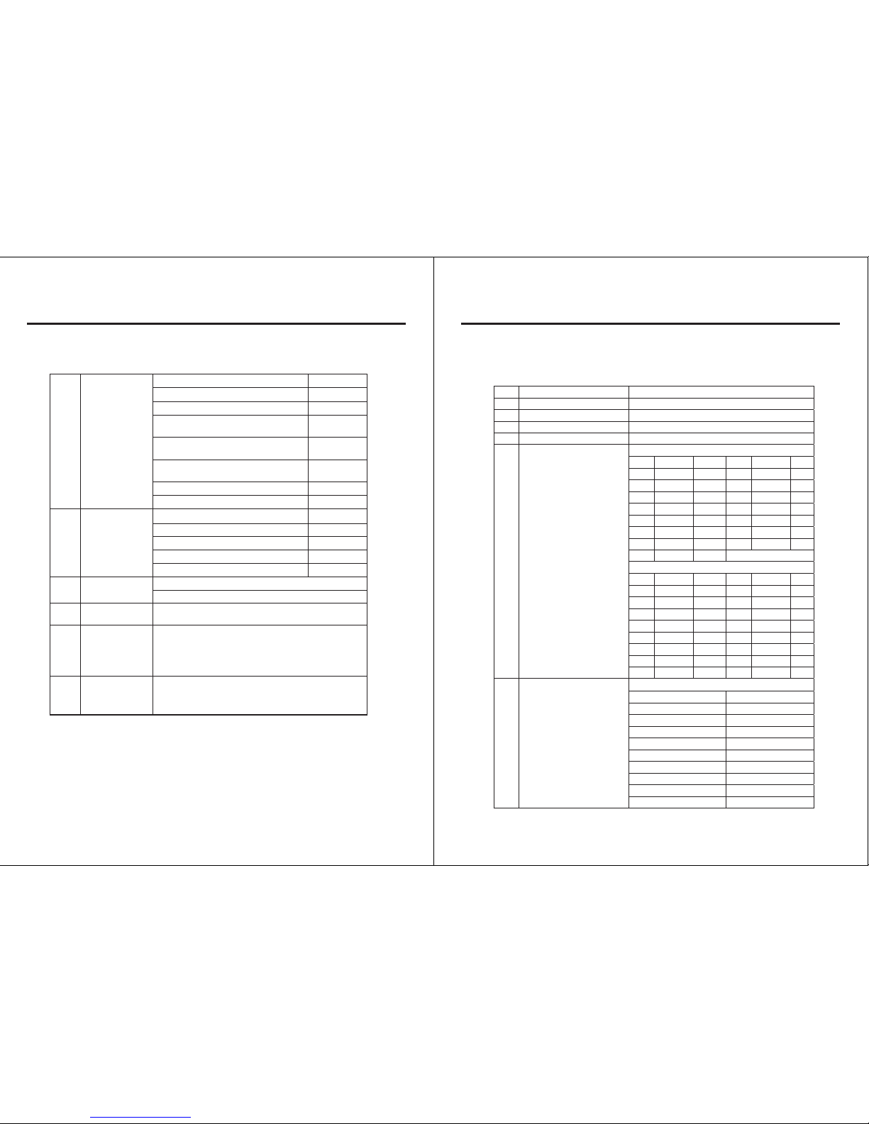
Table Of Contents
1. INTRODUCTION.................................................5
1.1 Purpose............................................................................................... 5
1.2 Regulatory Information ............................................................... 5
1.3 Abbreviations................................................................................... 7
2. PERFORMANCE..................................................9
2.1 H/W Features.................................................................................... 9
2.2 Technical Specification...............................................................11
3. TECHNICAL BRIEF............................................17
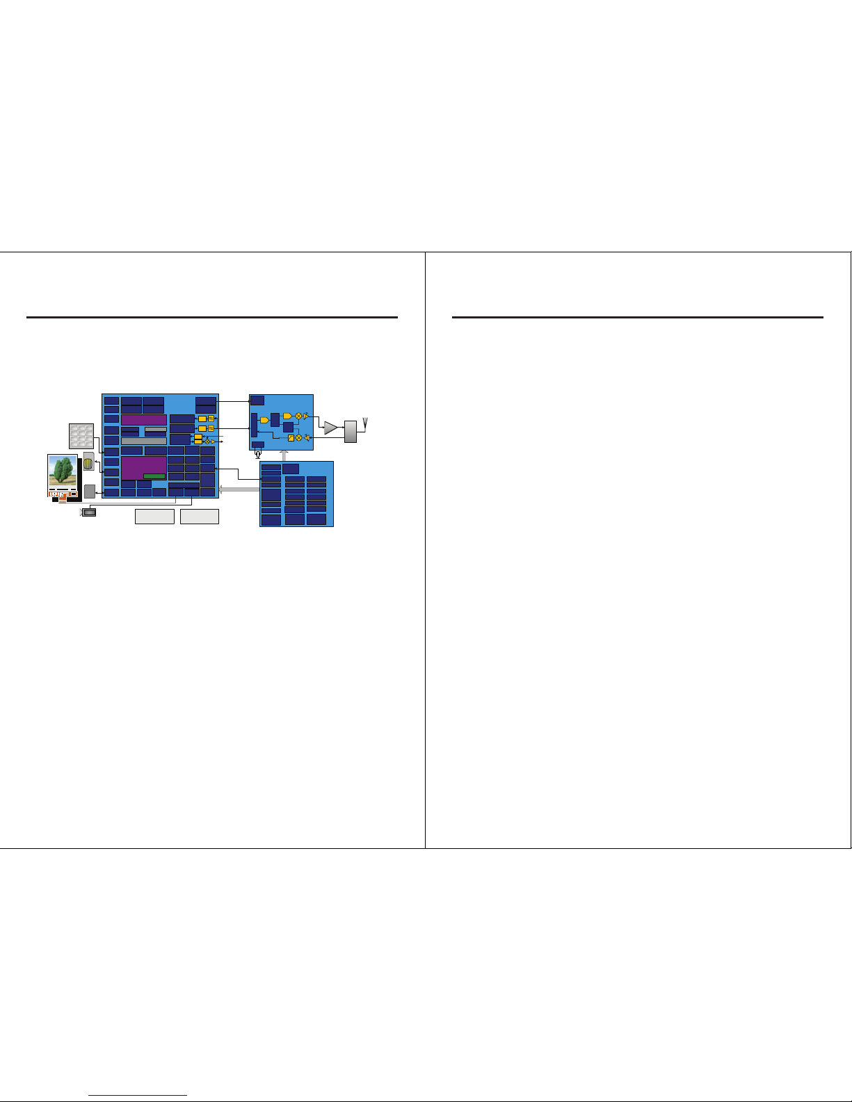
3.1 GS290 Functional Block diagram...........................................17
3.2 Baseband Processor (BBP) Introduction..............................18
3.3 Power management IC ..............................................................30
3.4. Power ON/OFF..............................................................................35
3.5. SIM & uSD interface....................................................................37
3.6. Memory...........................................................................................39
3.7. LCD Display....................................................................................40
3.8. Keypad Switching & Scanning...............................................41
3.9. Keypad back-light illumination .............................................42
3.10. LCD back-light illumination..................................................43
3.11. Audio..............................................................................................44
3.13. charging circuit..........................................................................46
3.14 FM radio & BLUETOOTH ..........................................................47
3.15. 5pin u-USB Interface connector..........................................51
3.16. General Description.................................................................54
3.17. Receiver part...............................................................................56
3.18. Transmitter part.........................................................................57
3.19. RF synthesizer.............................................................................58
3.20. Front End Module control .....................................................59
3.21. Power Amplifier Module........................................................60
3.22. PAM Schematic ..........................................................................61
4. TROUBLE SHOOTING ......................................62
4.1 Trouble shooting test setup.....................................................62
4.2 Power on Trouble..........................................................................63
4.3 Charging trouble ..........................................................................66
4.4 LCD display trouble .....................................................................68
4.5 Camera Trouble.............................................................................70
4.6 Receiver & Speaker trouble ......................................................72
4.7 Microphone trouble....................................................................75
4.8 Vibrator trouble.............................................................................77
4.9 Keypad back light trouble.........................................................79
4.10 SIM & uSD trouble......................................................................81
4.11 Touch trouble...............................................................................85
4.12 Trouble shooting of Receiver part.......................................87
4.13 Trouble shooting of Transmitter part.................................93
5. DOWNLOAD & S/W UPGRADE......................101
6. BLOCK DIAGRAM...........................................112
7. CIRCUIT DIAGRAM ........................................113
8. BGA Pin Map..................................................121
9. PCB LAYOUT...................................................129
10.ENGINEERING MODE...................................135
10.1.Test Equipment Setup..........................................................135
10.2. Calibration Step...................................................................... 135
11. STAND ALONE TEST ....................................140
11.1 Test Program Setting ............................................................. 140
11.2 Tx Test........................................................................................... 143
11.4 Rx Test.......................................................................................... 145
12. EXPLODED VIEW & REPLACEMENT
PART LIST ....................................................147
12.1 EXPLODED VIEW...................................................................... 147
12.2 Replacement Parts.................................................................. 149