LG 42LB9R-TA User manual

LCD TV
SERVICE MANUAL
CAUTION
BEFORE SERVICING THE CHASSIS,
READ THE SAFETY PRECAUTIONS IN THIS MANUAL.
CHASSIS : LP7BB
MODEL : 42LB9RTA 42LB9RTA-MB
website:htt ://biz.LGservice.com
Internal Use Only

- 2 -
Copyright©2007 LG Electronics. Inc. All right reserved.
Only for training and service p rposes
LGE Internal Use Only
CONTENTS
CONTENTS .............................................................................................. 2
SAFETY PRECAUTIONS ..........................................................................3
SPECIFICATION ........................................................................................6
ADJUSTMENT INSTRUCTION ...............................................................10
TROUBLE SHOOTING ............................................................................14
BLOCK DIAGRAM...................................................................................25
EXPLODED IEW .................................................................................. 26
S C. SHEET ...............................................................................................

- 3 -
Copyright©2007 LG Electronics. Inc. All right reserved.
Only for training and service p rposes
LGE Internal Use Only
SAFETY PRECAUTIONS
Many electrical and mechanical parts in this chassis have special safety-related characteristics. These parts are identified by in the
Schematic Diagram and Replacement Parts List.
It is essential that these special safety parts sho ld be replaced with the same components as recommended in this man al to prevent
Shock, Fire, or other Hazards.
Do not modify the original design witho t permission of man fact rer.
General Guidance
An isolation Transformer should always be used d ring the
servicing of a receiver whose chassis is not isolated from the AC
power line. Use a transformer of adeq ate power rating as this
protects the technician from accidents res lting in personal inj ry
from electrical shocks.
It will also protect the receiver and it's components from being
damaged by accidental shorts of the circ itry that may be
inadvertently introd ced d ring the service operation.
If any f se (or F sible Resistor) in this TV receiver is blown,
replace it with the specified.
When replacing a high wattage resistor (Oxide Metal Film Resistor,
over 1W), keep the resistor 10mm away from PCB.
Keep wires away from high voltage or high temperat re parts.
Before returning the receiver to the customer,
always perform an AC leakage current check on the exposed
metallic parts of the cabinet, s ch as antennas, terminals, etc., to
be s re the set is safe to operate witho t damage of electrical
shock.
Leakage Current Cold Check(Antenna Cold Check)
With the instr ment AC pl g removed from AC so rce, connect an
electrical j mper across the two AC pl g prongs. Place the AC
switch in the on position, connect one lead of ohm-meter to the AC
pl g prongs tied together and to ch other ohm-meter lead in t rn to
each exposed metallic parts s ch as antenna terminals, phone
jacks, etc.
If the exposed metallic part has a ret rn path to the chassis, the
meas red resistance sho ld be between 1MΩ and 5.2MΩ.
When the exposed metal has no ret rn path to the chassis the
reading m st be infinite.
An other abnormality exists that m st be corrected before the
receiver is ret rned to the c stomer.
Leakage Current Hot Check (See below Fig re)
Pl g the AC cord directly into the AC o tlet.
Do not use a line Isolation Transformer during this check.
Connect 1.5K/10watt resistor in parallel with a 0.15 F capacitor
between a known good earth gro nd (Water Pipe, Cond it, etc.)
and the exposed metallic parts.
Meas re the AC voltage across the resistor sing AC voltmeter
with 1000 ohms/volt or more sensitivity.
Reverse pl g the AC cord into the AC o tlet and repeat AC voltage
meas rements for each exposed metallic part. Any voltage
meas red m st not exceed 0.75 volt RMS which is corresponds to
0.5mA.
In case any meas rement is o t of the limits specified, there is
possibility of shock hazard and the set m st be checked and
repaired before it is ret rned to the c stomer.
Leakage Current Hot Check circuit
Replaceable batteries
1.5 Kohm/10W
To Instr ment's
exposed
METALLIC PARTS
Good Earth Gro nd
s ch as WATER PIPE,
CONDUIT etc.
AC Volt-meter
IMPORTANT SAFETY NOTICE
0.15 F
CAUTION
RISK OF EXPLOSION IF BATTERY
IS REPLACED BY AN INCORRECT
TYPE. DISPOSE OF USED
BATTERIES ACCORDING TO THE
INSTRUCTIONS
AD ARSEL
Lithi mbatteri - Eksplosionsfare ved
fejlagtig hándtening. Udskiftning má
k n ske med batteri at samme
fabrikat og type. Levér det br gte
batteri tilbage til leverandoren

- 4 -
Copyright©2007 LG Electronics. Inc. All right reserved.
Only for training and service p rposes
LGE Internal Use Only
CAUTION: Before servicing receivers covered by this service
man al and its s pplements and addenda, read and follow the
SAFETY PRECAUTIONS on page 3 of this p blication.
NOTE: If nforeseen circ mstances create conflict between the
following servicing preca tions and any of the safety preca tions on
page 3 of this p blication, always follow the safety preca tions.
Remember: Safety First.
General Servicing Preca tions
1. Always npl g the receiver AC power cord from the AC power
so rce before;
a. Removing or reinstalling any component, circ it board
mod le or any other receiver assembly.
b. Disconnecting or reconnecting any receiver electrical pl g or
other electrical connection.
c. Connecting a test s bstit te in parallel with an electrolytic
capacitor in the receiver.
CAUTION: A wrong part s bstit tion or incorrect polarity
installation of electrolytic capacitors may res lt in an
explosion hazard.
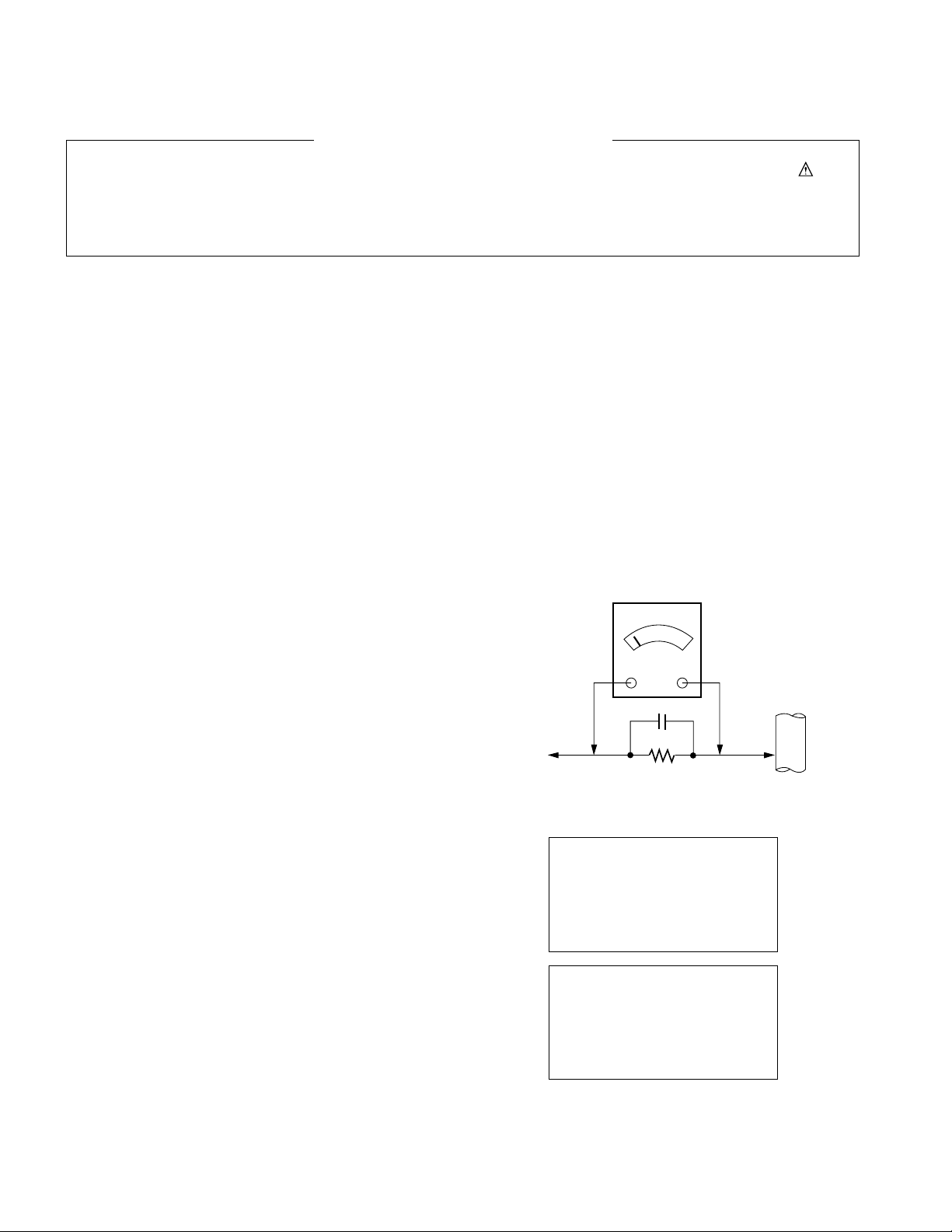
2. Test high voltage only by meas ring it with an appropriate high
voltage meter or other voltage meas ring device (DVM,
FETVOM, etc) eq ipped with a s itable high voltage probe.
Do not test high voltage by "drawing an arc".
3. Do not spray chemicals on or near this receiver or any of its
assemblies.
4. Unless specified otherwise in this service man al, clean
electrical contacts only by applying the following mixt re to the
contacts with a pipe cleaner, cotton-tipped stick or comparable
non-abrasive applicator; 10% (by vol me) Acetone and 90% (by
vol me) isopropyl alcohol (90%-99% strength)
CAUTION: This is a flammable mixt re.
Unless specified otherwise in this service man al, l brication of
contacts in not req ired.
5. Do not defeat any pl g/socket B+ voltage interlocks with which
receivers covered by this service man al might be eq ipped.
6. Do not apply AC power to this instr ment and/or any of its
electrical assemblies nless all solid-state device heat sinks are
correctly installed.
7. Always connect the test receiver gro nd lead to the receiver
chassis gro nd before connecting the test receiver positive
lead.
Always remove the test receiver gro nd lead last.
8. Use with this receiver only the test fixtures s ecified in this
service manual.
CAUTION: Do not connect the test fixt re gro nd strap to any
heat sink in this receiver.
Electrostatically Sensitive (ES) Devices
Some semicond ctor (solid-state) devices can be damaged easily
by static electricity. S ch components commonly are called
Electrostatically Sensitive (ES) Devices. Examples of typical ES
devices are integrated circ its and some field-effect transistors and
semicond ctor "chip" components. The following techniq es
sho ld be sed to help red ce the incidence of component
damage ca sed by static by static electricity.
1. Immediately before handling any semicond ctor component or
semicond ctor-eq ipped assembly, drain off any electrostatic
charge on yo r body by to ching a known earth gro nd.
Alternatively, obtain and wear a commercially available
discharging wrist strap device, which sho ld be removed to
prevent potential shock reasons prior to applying power to the
nit nder test.
2. After removing an electrical assembly eq ipped with ES
devices, place the assembly on a cond ctive s rface s ch as
al min m foil, to prevent electrostatic charge b ild p or
expos re of the assembly.
3. Use only a gro nded-tip soldering iron to solder or nsolder ES
devices.
4. Use only an anti-static type solder removal device. Some solder
removal devices not classified as "anti-static" can generate
electrical charges s fficient to damage ES devices.
5. Do not se freon-propelled chemicals. These can generate
electrical charges s fficient to damage ES devices.
6. Do not remove a replacement ES device from its protective
package ntil immediately before yo are ready to install it.
(Most replacement ES devices are packaged with leads
electrically shorted together by cond ctive foam, al min m foil
or comparable cond ctive material).
7. Immediately before removing the protective material from the
leads of a replacement ES device, to ch the protective material
to the chassis or circ it assembly into which the device will be
installed.
CAUTION: Be s re no power is applied to the chassis or circ it,
and observe all other safety preca tions.
8. Minimize bodily motions when handling npackaged
replacement ES devices. (Otherwise harmless motion s ch as
the br shing together of yo r clothes fabric or the lifting of yo r
foot from a carpeted floor can generate static electricity
s fficient to damage an ES device.)
General Soldering G idelines
1. Use a gro nded-tip, low-wattage soldering iron and appropriate
tip size and shape that will maintain tip temperat re within the
range or 500°F to 600°F.
2. Use an appropriate ga ge of RMA resin-core solder composed
of 60 parts tin/40 parts lead.
3. Keep the soldering iron tip clean and well tinned.
4. Thoro ghly clean the s rfaces to be soldered. Use a mall wire-
bristle (0.5 inch, or 1.25cm) br sh with a metal handle.
Do not se freon-propelled spray-on cleaners.
5. Use the following nsoldering techniq e
a. Allow the soldering iron tip to reach normal temperat re.
(500°F to 600°F)
b. Heat the component lead ntil the solder melts.
c. Q ickly draw the melted solder with an anti-static, s ction-
type solder removal device or with solder braid.
CAUTION: Work q ickly to avoid overheating the circ it
board printed foil.
6. Use the following soldering techniq e.
a. Allow the soldering iron tip to reach a normal temperat re
(500°F to 600°F)
b. First, hold the soldering iron tip and solder the strand against
the component lead ntil the solder melts.
c. Q ickly move the soldering iron tip to the j nction of the
component lead and the printed circ it foil, and hold it there
only ntil the solder flows onto and aro nd both the
component lead and the foil.
CAUTION: Work q ickly to avoid overheating the circ it
board printed foil.
d. Closely inspect the solder area and remove any excess or
splashed solder with a small wire-bristle br sh.
SER ICING PRECAUTIONS

- 5 -
Copyright©2007 LG Electronics. Inc. All right reserved.
Only for training and service p rposes
LGE Internal Use Only
IC Remove/Replacement
Some chassis circ it boards have slotted holes (oblong) thro gh
which the IC leads are inserted and then bent flat against the
circ it foil. When holes are the slotted type, the following techniq e
sho ld be sed to remove and replace the IC. When working with
boards sing the familiar ro nd hole, se the standard techniq e
as o tlined in paragraphs 5 and 6 above.
Removal
1. Desolder and straighten each IC lead in one operation by gently
prying p on the lead with the soldering iron tip as the solder
melts.
2. Draw away the melted solder with an anti-static s ction-type
solder removal device (or with solder braid) before removing the
IC.
Re lacement
1. Caref lly insert the replacement IC in the circ it board.
2. Caref lly bend each IC lead against the circ it foil pad and
solder it.
3. Clean the soldered areas with a small wire-bristle br sh.
(It is not necessary to reapply acrylic coating to the areas).
"Small-Signal" Discrete Transistor
Removal/Replacement
1. Remove the defective transistor by clipping its leads as close as
possible to the component body.
2. Bend into a "U" shape the end of each of three leads remaining
on the circ it board.
3. Bend into a "U" shape the replacement transistor leads.
4. Connect the replacement transistor leads to the corresponding
leads extending from the circ it board and crimp the "U" with
long nose pliers to ins re metal to metal contact then solder
each connection.
Power Output, Transistor Device
Removal/Replacement
1. Heat and remove all solder from aro nd the transistor leads.
2. Remove the heat sink mo nting screw (if so eq ipped).
3. Caref lly remove the transistor from the heat sink of the circ it
board.
4. Insert new transistor in the circ it board.
5. Solder each transistor lead, and clip off excess lead.
6. Replace heat sink.
Diode Removal/Replacement
1. Remove defective diode by clipping its leads as close as
possible to diode body.
2. Bend the two remaining leads perpendic lar y to the circ it
board.
3. Observing diode polarity, wrap each lead of the new diode
aro nd the corresponding lead on the circ it board.
4. Sec rely crimp each connection and solder it.
5. Inspect (on the circ it board copper side) the solder joints of
the two "original" leads. If they are not shiny, reheat them and if
necessary, apply additional solder.
Fuse and Conventional Resistor
Removal/Replacement
1. Clip each f se or resistor lead at top of the circ it board hollow
stake.
2. Sec rely crimp the leads of replacement component aro nd
notch at stake top.
3. Solder the connections.
CAUTION: Maintain original spacing between the replaced
component and adjacent components and the circ it board to
prevent excessive component temperat res.
Circuit Board Foil Repair
Excessive heat applied to the copper foil of any printed circ it
board will weaken the adhesive that bonds the foil to the circ it
board ca sing the foil to separate from or "lift-off" the board. The
following g idelines and proced res sho ld be followed whenever
this condition is enco ntered.
At IC Connections
To repair a defective copper pattern at IC connections se the
following proced re to install a j mper wire on the copper pattern
side of the circ it board. (Use this techniq e only on IC
connections).
1. Caref lly remove the damaged copper pattern with a sharp
knife. (Remove only as m ch copper as absol tely necessary).
2. caref lly scratch away the solder resist and acrylic coating (if
sed) from the end of the remaining copper pattern.
3. Bend a small "U" in one end of a small ga ge j mper wire and
caref lly crimp it aro nd the IC pin. Solder the IC connection.
4. Ro te the j mper wire along the path of the o t-away copper
pattern and let it overlap the previo sly scraped end of the good
copper pattern. Solder the overlapped area and clip off any
excess j mper wire.
At Other Connections
Use the following techniq e to repair the defective copper pattern
at connections other than IC Pins. This techniq e involves the
installation of a j mper wire on the component side of the circ it
board.
1. Remove the defective copper pattern with a sharp knife.
Remove at least 1/4 inch of copper, to ens re that a hazardo s
condition will not exist if the j mper wire opens.
2. Trace along the copper pattern from both sides of the pattern
break and locate the nearest component that is directly
connected to the affected copper pattern.
3. Connect ins lated 20-ga ge j mper wire from the lead of the
nearest component on one side of the pattern break to the lead
of the nearest component on the other side.
Caref lly crimp and solder the connections.
CAUTION: Be s re the ins lated j mper wire is dressed so the
it does not to ch components or sharp edges.

- 6 -
Copyright©2007 LG Electronics. Inc. All right reserved.
Only for training and service p rposes
LGE Internal Use Only
1. Application range
This spec sheet is applied to the LCD TV sed LP7BB
chassis
2. Specification
Each part is tested as below witho t special appointment.
(1) Temperat re : 25 ± 5°C(77 ± 9°F), CST : 40 ± 5°C
(2) Relative H midity : 65% ± 10%
(3) Power Voltage : Standard inp t voltage (100-240V~,
50/60Hz)
*Standard Voltage of each prod cts is marked by models
(4) Specification and performance of each parts are followed
each drawing and specification by part n mber in
accordance with BOM.
(5) The receiver m st be operated for abo t 20 min tes prior
to the adj stment.
3. Test method
(1) Performance : LGE TV test method followed
(2) Demanded other specification
Safety : CE, IEC Specification
EMC : CE, IEC
SPECIFICATION
NOTE : Specifications and others are s bject to change witho t notice for improvement
.
4. General T Specification
No Item Specification Remark
1. Video inp t applicable system NTSC-M, PAL M/N
2. Receivable Broadcasting System 1) NTSC
2) PAL M
3) PAL N
3. RF Inp t Channel BAND NTSC
VHF 2 ~ 13
UHF 14 ~ 69
CATV 1 ~ 125
4. Inp t Voltage 100-240V~ / 50Hz, 60Hz
5. Market Central & So th America
6. Operating Environment 1) Temp : 0 ~ 40 deg
2) H midity : 10 ~ 90 %RH
7. Storage Environment 1) Temp : -20 ~ 50 deg
2) H midity : 10 ~ 90 %RH
8. Power Cons mption Power on ≤ 260(42”)
(Green) ≤ 220(32”)
9. Stand by Cool ≤ 1W(32”, 42”)
Warm ≤ 40W(32”, 42”) When recordign the man al recording
10. Freq ency range H : 31 ~ 61 khz PC Inp t
V : 56 ~ 75 Hz
11. Video Inp t (2EA) NTSC, PAL M/N
12. S-Video Inp t (1EA) NTSC, PAL M/N Side only
13. Component Inp t (2EA) Y/Cb/Cr, Y/Pb/Pr
14. RGB Inp t (1EA) RGB-PC
15. HDMI Inp t (2EA) HDMI-PC
HDMI-DTV
16. A dio Inp t (5EA) PC A dio, Component (2EA), AV(2EA) L/R Inp t
17. A dio variable o t (1EA)
18. USB Inp t (1EA) DivX, MP3, JPEG
19. AV o t (1EA)

- 7 -
Copyright©2007 LG Electronics. Inc. All right reserved.
Only for training and service p rposes
LGE Internal Use Only
5. General Module Specification
No Item Specification Remark
1 . Panel 42" TFT WXGA LCD
32" TFT WXGA LCD
2. LCD Mod le O tline 42" 983 x 576 x 47.3 (H)mm x (V)mm x (D)mm
Dimension 32" 760.0 x 450.0 x 48.0
Pixel Pitch 42" 0.227 x 0.681 x RGB mm
32" 0.17025 x 0.51075 x RGB
Pixel Format 1366 x 768 Pixels RGB strip arrangement
Coating Hard coating(3H), Anti-glare treatment
of the front polarizer,
Back Light 42" 18CCFL
32" 18CCFL
6. Set Optical Feature (LCD Module)
No Item Min Typ Max Unit Maker Remark
1. L minance 400 500 LPL(0RT) - 50cm from the s rface
32",42" - F ll White Pattern
2. View angle (R/L, U/D) 178/178 degree LPL 32”, 42” - CR > 10
3. White White X -0.03 0.279/0.279/0.279 +0.03
coordinate Y 0.292/0.292/0.292
Red X 0.635/0.636/0.635
Y 0.339/0.343/0.344
Green X 0.282/0.284/0.286
Y 0.606/0.615/0.614
Bl e X 0.145/0.144/0.146
Y 0.064/0.063/0.061
4. Contrast ratio CR 600 800 32" LPL(0-RT)
800 1000 42" LPL(0-RT)
5. L minance Variation 1.3

- 8 -
Copyright©2007 LG Electronics. Inc. All right reserved.
Only for training and service p rposes
LGE Internal Use Only
7. Component ideo Input (Y, PB, PR)
No Resol tion H-freq(kHz) V-freq.(kHz) Pixel clock(MHz) Remarks
1. 720*480 15.73 59.94 13.500 SDTV, DVD 480I(525I)
720*480 15.75 60.00 13.514 SDTV, DVD 480I(525I)
2. 720*576 15.625 50.00 13.500 SDTV, DVD 576I(625I)
3. 720*480 31.47 59.94 27.000 SDTV 480P
720*480 31.50 60.00 27.027 SDTV 480P
4. 720*576 31.25 50.00 27.000 SDTV 576P
5. 1280*720 44.96 59.94 74.176 HDTV 720P
1280*720 45.00 60.00 74.250 HDTV 720P
6. 1280*720 37.50 50.00 74.25 HDTV 720P 50Hz
7. 1920*1080 33.72 59.94 74.176 HDTV 1080I
1920*1080 33.75 60.00 74.250 HDTV 1080I
8. 1920*1080 28.125 50.00 74.250 HDTV 1080I 50Hz,
9. 1920*1080 67.5 60.00 148.5 HDTV 1080P
10. 1920*1080 56.25 50 148.5 HDTV 1080P 50Hz
8. RGB Input ( PC )
No Resol tion H-freq(kHz) V-freq.(kHz) Pixel clock(MHz) Remarks
1 720*400 31.469 70.08 28.32 DOS
2. 640*480 31.469 59.94 25.17 VESA(VGA)
3 640*480 37.500 75.00 31.50 VESA(VGA)
4 800*600 37.879 60.31 40.00 VESA(SVGA)
5 800*600 46.875 75.00 49.50 VESA(SVGA)
6 1024*768 48.363 60.00 65.00 VESA(XGA)
7 1024*768 56.476 70.06 78.75 VESA(XGA)
8 1024*768 60.023 75.02 79.50 VESA(XGA)
9 1280*768 47.776 59.87 80.125 WXGA(42XGA,50",60")
10 1360*768 47.712 60.01 85.50 WXGA(42XGA,50",60")
11 1366*768 47.700 60.00 84.62 WXGA(42XGA,50",60")
9. HDMI Input ( PC )
No Resol tion H-freq(kHz) V-freq.(kHz) Pixel clock(MHz) Remarks
1 720*400 31.469 70.08 28.32 DOS
2 640*480 31.469 59.94 25.17 VESA(VGA)
3 640*480 37.500 75.00 31.50 VESA(VGA)
4 800*600 37.879 60.31 40.00 VESA(SVGA)
5 800*600 46.875 75.00 49.50 VESA(SVGA)
6 1024*768 48.363 60.00 65.00 VESA(XGA)
7 1024*768 56.476 70.06 75.00 VESA(XGA)
8 1024*768 60.023 75.02 78.75 VESA(XGA)
9 1280*768 47.776 59.87 79.50 WXGA(42XGA,50",60")
10 1360*768 47.712 60.01 85.50 WXGA(42XGA,50",60")
11 1366*768 47.700 60.00 84.62 WXGA(42XGA,50",60")

- 9 -
Copyright©2007 LG Electronics. Inc. All right reserved.
Only for training and service p rposes
LGE Internal Use Only
10. HDMI input ( DT )
No Resol tion H-freq(kHz) V-freq.(kHz) Pixel clock(MHz) Remarks
1. 720*480 31.47 59.94 27.000 SDTV 480P
2. 720*480 31.50 60.00 27.027 SDTV 480P
3. 720*576 31.25 50.00 27.000 SDTV 576P
4. 1280*720 44.96 59.94 74.176 HDTV 720P
5. 1280*720 45.00 60.00 74.250 HDTV 720P
6. 1280*720 37.50 50.00 74.25 HDTV 720P 50H
7. 1920*1080 33.72 59.94 74.176 HDTV 1080I
8. 1920*1080 33.75 60.00 74.250 HDTV 1080I
9. 1920*1080 28.125 50.00 74.250 HDTV 1080I 50Hz
10. 1920*1080 67.5 60.00 148.5 HDTV 1080P
11. 1920*1080 56.25 50 148.5 HDTV 1080P 50Hz

- 10 -
Copyright©2007 LG Electronics. Inc. All right reserved.
Only for training and service p rposes
LGE Internal Use Only
ADJUSTMENT INSTRUCTION
1. Application Range
This spec. sheet is applied to all of the LP7BB chassis
(Sat rn Analog DVR) man fact red at LG TV Plant all over
the world.
2. Specification
2.1 Beca se this is not a hot chassis, it is not necessary to
se an isolation transformer.
However, the se of isolation transformer will help to
protect test instr ments.
2.2 Adj stment m st be done in the correct seq ence.
2.3 The adj stment m st be performed at 25±5°C
temperat re and 65±10% relative h midity if there is no
specified designation.
2.4 The inp t voltage of the receiver m st be kept between
100-220V, 50/60Hz.
2.5 Before adj stment, exec te Heat-R n for 30 min tes at
F ll White mode.(Power on key)
3. PCB assembly adjustment items
* Channel memory
- Download the channel data from BOM to EEPROM by
sing LGIDS.
* Option adj stment following BOM
- Tool Option1
- Tool Option2
- Area Option
(Fig.1)
1) P sh the ADJ key in the Adj st Remocon.
2) Inp t the Option N mber that was specified in the BOM,
into the Shipping area.
3) Select "Tool Option1/ Tool Option2/ Area Option" by sing
(CH+/-) key , and press the n mber key(0~9)
consec tively
ex) If the val e of Tool Option1 is 7, inp t the data sing
n mber key "7" (Fig. 1)
4. SET assembly adjustment items
A to AV Color Balance
Adj stment of White Balance
A to Component Color Balance adj stment
- Standard eq ipment : MSPG925FA
A to RGB Color Balance adj stment
- Standard eq ipment : MSPG925FA
(At DVR model Case, Please check DVR f nction like
following list )
Checking DVR F nction and HDD
Check DVR F nction as follow on 4.2 and find HDD fail re
nder malf nction.
5. HDD Assembly Adjustment method
5.1. HDD FORMAT
1) Assemble MAIN , DVR Board.
2) HDD Format in progress words will create a tomatically.
3) Please, wait for 30~40 seconds.
5.1.1. HDD Format in progress
5.1.2. HDD Format completed
5.2. S b Program Download for "DVR" by sing USB
memory stick
1) connect USB memory stick to SET
2) Set power off -> ON
- DVR s/w will be installed a tomatically
LP7BA LPL 42 Normal
S/W Version X.XX
DVR Version X.XX
UTT XX hr
Tool Option1 7
Tool Option2 161
Area Option 16
:

- 11 -
Copyright©2007 LG Electronics. Inc. All right reserved.
Only for training and service p rposes
LGE Internal Use Only
6. EDID
Ca tion
* Use the proper signal cable for EDID Download
- Analog EDID : Pin3 exists
- Digital EDID : Pin3 exists
=> Ca tion : - Never connect HDMI & DVI-D & DVI-A Cable
at the same time.
- Use the proper cables below for EDID Writing
6.1. Data
6.1.1 ANALOG(256 Bytes )
BLOCK1 (128BYTE)
6.1.2 HDMI(256 Bytes )
BLOCK1 (128BYTE)
BLOCK2 (128BYTE)
7. ADC Calibration
=> Ca tion : - System control RS-232 Host sho ld be "PC"
for adj stment.
Press the FRONT-AV KEY on R/C for converting inp t
mode.
(change RS-232 Host : pc, Band Rate : 115200bps)
7.1 Adj stment of RF/AV/S-VIDEO
* Req ired Eq ipments
- Remote controller for adj stment
- 802F Pattern Generator, Master (MSPG-925FA), etc.
- MSPG-925FA Pattern Generator
(Which has Video Signal: 100% Color Bar Pattern
shown in Fig. 2)
=> Model: 202 / Pattern : 65
(Fig. 2)
7.1.1 Method of A to RF/AV/S-VIDEO Color Balance.
1) Press the FRONT-AV KEY on R/C for converting inp t
mode.
2) Inp t the Video Signal: 100% Color Bar signal into AV
3) Set the PSM to Dynamic mode in the Pict re men .
4) Press INSTART key on R/C for adj stment.
5) Press the (Vol. +) key to operate the set, then it
becomes a tomatically
6) A to-RGB OK means the adj stment is completed
7.1.2 Req irement
- This AV color balance adj stment sho ld be performed
before White Balance Adj stment.
- After AV color balance adj stment, Change the mode
from AV to RF.
(Cancel Heat-r n mode.)
ADC RF/AV/S-VIDEO Component RGB
MSPG925FA PAL NTSC Model:217 720P Model: 60
INPUT AV3-ZF VIDEO1 -MA Pattern:65 1024*768 60Hz
SELECT
AV1-TB
* 100% Color Bar
Pattern: 65
Model: 202 Model:201
* 100% Color Bar
(PAL-BGDHI) (NTSC)
Pattern: 65 Pattern: 65
* 100% Color Bar * 100% Color Bar

- 12 -
Copyright©2007 LG Electronics. Inc. All right reserved.
Only for training and service p rposes
LGE Internal Use Only
7.2 Adj stment of Component.
* Req ired Eq ipments
- Remote controller for adj stment
- 802F Pattern Generator, Master (MSPG-925FA), etc
- MSPG-925FA Pattern Generator
(Which has 720p@60Hz YPbPr signal : 100% Color
Bar Pattern shown in Fig. 3 )
=> Model: 217 / Pattern: 65
- It is very import to se correct adj stment pattern like
Fig.3.
a. Within the pattern, color seq ence sho ld be aligned
: White-Yellow-Cyan-Green-Magenta-Red-BLUE-
BLACK
(If color seq ence is reversed (Black -> …-> White),
reverse the pattern with REV key, when sing Master
pattern generator like MSPG-925)
b. If Minim m Black Level and/or Maxim m White Level
is not correct, Do select 100% Color Bar Pattern.
(Fig. 3)
7.2.1 Method of A to Component Color Balance
1) Inp t the Component 720p 100% Color Bar(MSPG-
925FA model:217, pattern:65) signal into Component.
(MH : component 1 )
2) Set the PSM to Dynamic mode in the Pict re men
3) Press the INSTART key on R/C for adj stment
4) Press the (Vol. +) key to operate the set, then it
becomes a tomatically
5) A to-RGB OK means the adj stment is completed
7.3 Adj stment of RGB
* Req ired Eq ipments
- Remote controller for adj stment
- 802F Pattern Generator, Master (MSPG-925FA), etc
- MSPG-925FA Pattern Generator
(Which has XGA [1024*768] 60Hz PC Format o tp t
signal : 100% Color Bar Pattern shown in Fig. 4 )
- It is very import to se correct adj stment pattern like
Fig. 4.
a. Within the pattern, color seq ence sho ld be aligned
: White-Yellow-Cyan-Green-Magenta-Red-BLUE-
BLACK
(If color seq ence is reversed (Black -> …-> White),
reverse the pattern with REV key, when sing Master
pattern generator like MSPG-925)
b. If Minim m Black Level and/or Maxim m White Level
is not correct, Do select 100% Color Bar Pattern
(Fig. 4)
7.3.1 Method of A to RGB Color Balance
1) Inp t the PC 1024x768 @ 60Hz with 100% color bar
pattern like Fig.4. into RGB.
(Ex. MSPG-925FA, model:60, pattern:65)
2) Set the PSM to Dynamic mode in Pict re men
3) Press the INSTART key on R/C for adj stment
4) Press the (Vol. +) key operate To set , then it
becomes a tomatically
5) A to-RGB OK means adj stment is completed

- 13 -
Copyright©2007 LG Electronics. Inc. All right reserved.
Only for training and service p rposes
LGE Internal Use Only
8. White Balance
* Ca tion : Before White-balance, the AV ADC sho ld be done.
=> Notice
- Do the white balance adj stment nder the 10LUX
- Before white balance, press the In-start key 2times and do
the reset like Fig.5
- Use the Torino inner pattern(216 gray pattern)
- To enter White-balance mode,press the IN-START key
2times.
* Ca tion : - System control RS-232 Host sho ld be "PC" for
adj stment.
(Fig. 4)
* Test Eq ipment
LCD : Color Analyzer ( CA-110), PDP : Color Analyzer (CA-
100)
CA-210 : The both of LCD and PDP are available.
PC (for comm nication thro gh RS-232C) -> UART Ba d
rate : 115200
Pattern Generator (MSPG-925FA etc. )
* Color Temperat re & Color Coordinates Setting
When adj sting the Color Temperat re of LCD, Color
AnalyzerCA-210(Matrix sho ld be corrected thro gh CH9 of
CS-1000) sho ld be sed.
When adj sting the Color Temperat re of PDP, Color
AnalyzerCA-210(Matrix sho ld be corrected thro gh CH10
of CS-1000) sho ld be sed.
Adj st the Color Temperat re based below adj stment color
coordinates.
Even if CH9 of CA-210 is corrected with Matrix, there may
be many character of Mod le and Filter.
Therefore Refer to the below Color Coordinates Target.
B t, in case of WCG mod le, se the CH12 of CA-210.
White Balance(Hex)
Color Temp. Cool
Red Gain. 80
Green Gain. 80
Bl e Gain. 80
Red Offset 80
Green Offset 80
Bl e Offset 80
Reset _ To set

- 14 -
Copyright©2007 LG Electronics. Inc. All right reserved.
Only for training and service p rposes
LGE Internal Use Only
TROUBLESHOOTING
1. No power
Symptom
1) Min te discharg e doesn't occ r at mod le.
2) Front LED doesn't come into action.
Start check
Is inserted a pl g
in power cord?
Is connected the Line
Filter and PSU?
Is normal the f se of
PSU? Plasma (F101),
LCD(F111 )
Pl g in a power cord
Connect a cable.
Plasma (EL11), LC D(SC100 )
Replace the f se
Is it connected tha t
PSU and 13 pin cable
in VSC board ?
Connect the 13pin cable.
YE S
YE S
YE S
YE S
NO
NO
NO
NO
After remo ve all cab les con nec ted to
PSU (except the C N101) , a thor izes the AC
vo ltage marking on man al.
When ST -by 5V doesn't operate , replace PSU

- 15 -
Copyright©2007 LG Electronics. Inc. All right reserved.
Only for training and service p rposes
LGE Internal Use Only
Symptom
1) After once shining, it doesn't discharge min tely from mod le.
2) The relay falls. ( The so nd is a dible "Click")
3) It is converted w ith the co lor where the front LED is red from gr een .
2. Protection mode
Start check
Is the PSU
no rmal?
Is the each
connector norma l?
Is t he Y- Board
no rmal ?
Is o tp t the no rmality Low/High
Voltage except Stand-by 5V? Replace the power board
After connecting we ll each
connector the normality it operates? Replace the power board
Is no rmal the o tp t voltage after
remove P1 connector of Y-B/D? Replace Y-B/D
Is no rmal the f se
(FS2 ,FS3 ) on Y-B/D?
Replace the f se
Is the Z - Board
no rmal ?
Is no rmal the o tp t vo ltage after
remove P1 connector of Z-B/D? Replace Z -B/D
Is no rmal the f se
(FS1 ,FS2 ) on Z-B/D?
Replace the f se
Is t he X- Board
no rmal ?
After remove P100,110 o tp t voltage normality:
Re place Ri ght X-B/ D
Afte r remo ve P200,210 o tp t voltage normality:
Replace Left X- B/D
Is normal the o tp t voltage
after remove P100,110,200, 210
connector of X- B/D?
YE S
YE S
YE S
YE S
YE S
YE S
NO
NO
NO
NO
NO
NO
NO

- 16 -
Copyright©2007 LG Electronics. Inc. All right reserved.
Only for training and service p rposes
LGE Internal Use Only
3. No Raster
Sy mptom
1) No OSD and image occ r at screen.
2) It maintains the condition where the front LED is green
Start check
Is the link cable
normal?
Reconnect the link cable
in P600
NO
Is the IC700's
o tp t normal?
NO Replace the VSC
Does min te
discharge at
Mod le?
NO Is the
inverter/ VaV s
on?
Check the PDP/LCD Mod le
Is o tp t the normality Low/High
Voltage except Stand-by 5V?
Replace
the power board
YE S
YE S
YE S
NO

- 17 -
Copyright©2007 LG Electronics. Inc. All right reserved.
Only for training and service p rposes
LGE Internal Use Only
4. In case of becomes unusual display from RF mode(Main)
A
Is normal video o tp t
of the T ner?
(Check TU200_Pin14)
Is normal the I2C comm nication ?
(Check Pin5, Pin4)
Is normal the Inp t voltage ?
(Check L308)
Is normal the Inp t voltage ?
(Check Pin8, Pin6)
Is normal video
o tp t of CXA2069Q?
(Check R324, In case of S-Video
check R324, R328)
Is the T ner Cable
connected well?
Change the T nerCheck the powerCable inserts well.
Is normal the
I2C comm nication ?
(Check R309, R310)
Change the IC(IC300)
Check the power
( Check L1004)
Change the IC(IC700)
Is the LVDS Cable
connected well? Cable inserts well
NO NO NO
YE S
NO YE S YES
YE S
YE S
YE S
NO
NO NO
NO

- 18 -
Copyright©2007 LG Electronics. Inc. All right reserved.
Only for training and service p rposes
LGE Internal Use Only
5. In the case of becomes unusual display from rear A mode(main)
6. In the case of becomes unusual display from rear S- ideo mode(main)
7. In the case of becomes unusual display from side A mode(main)
Is normal video inp t
of the A/V jack?
Is normal video inp t
of the A/V jack?
Is normal video inp t
of the A/V jack? Check the inp t so rce
Same as Block A
Same as Block A
Same as Block A
Check the inp t so rce
YES
NO
YES
NO
YES
NO

- 19 -
Copyright©2007 LG Electronics. Inc. All right reserved.
Only for training and service p rposes
LGE Internal Use Only
8. In the case of becomes unusual display from side S- ideo mode(main)
Is normal video inp t
of the A/V jack?
(Check R339, R341, L310)
Check the inp t so rce
Same as Block A
YES
NO

- 20 -
Copyright©2007 LG Electronics. Inc. All right reserved.
Only for training and service p rposes
LGE Internal Use Only
13. In case of becomes unusual display from RF mode(Sub)
Is normal video o tp t
of the T ner?
(Check TU201_Pin14)
Is normal the I2C comm nication ?
(Check Pin5, Pin4)
Is normal video
o tp t of CXA2069Q?
(Check R312, In case of S-Video
check R312, R314)
Is the T ner Cable
connected well?
Is normal the Inp t voltage ?
(Check Pin8, Pin6)
Is normal the Inp t voltage ?
(Check L308)
Is normal the
I2C comm nication ?
(Check R309, R310)
Change the IC(IC300)
Check the power
( Check L1004)
Change the IC(IC700)
Is the LVDS Cable
connected well? Cable inserts well
Change the T ner
Check the power
( L1103)
Cable inserts well.
B
NO
NO NO
NO NONO
NO
YES
YES
YES
YES YES
YES YES
14. In case PIP doesn't display from other modes(Sub)
Same as the case of main except block A sho ld be change to B
This manual suits for next models
1
Table of contents
Other LG LCD TV manuals