Linear 1351A User manual

QUICK START GUIDE FOR DEMONSTRATION CIRCUIT 1351A
SINGLE OUTPUT, HIGH POWER, HIGH EFFICIENCY POE
1
LTC4269IDKD-2
DESCRIPTION
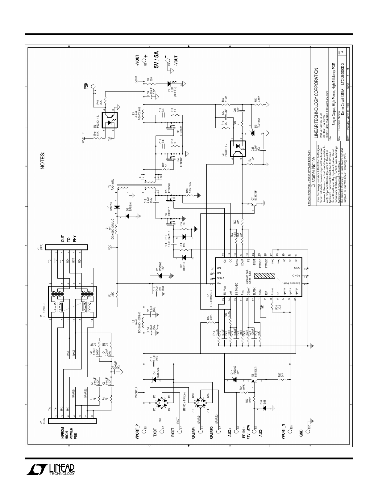
Demonstration circuit 1351A is a high-power supply
featuring the LTC®4269IDKD-2. This board acts as
an IEEE 802.3at compliant, high power Power-over-
Ethernet (PoE), Powered Device (PD) and connects
at the RJ45 to a compatible high power Power
Sourcing Equipment (PSE) device, such as the
DC1366A.
The LTC4269IDKD-2 provides IEEE802.3at standard
(PoE+) PD interfacing and power supply control.
When the PD is fully powered, the PD interface
switches power over from the PSE to the switcher
through an internal, low resistance, high power
MOSFET. The highly integrated LTC4269IDKD-2 con-
trols a high-power, small-sized power supply that
utilizes a highly-efficient isolated forward topology
with synchronous rectification. The DC1351A sup-
plies a 5V output at up to 5A.
DC1351A also demonstrates the use of an auxiliary
48V wall adapter. When present, the auxiliary supply
becomes the dominant supply over PoE to provide
power.
Design files for this circuit board are available.
Call the LTC factory.
,LTC and LT are registered trademarks of Linear Technology Corporation.
Table 1.
Performance Summary (TA= 25°C)
PARAMETER CONDITION VALUE
Port Voltage (V
PORT
) At Ethernet port 37V – 57V
Auxiliary Voltage (V
AUX
) From Aux- to Aux+ terminals 44V – 57V
Output Voltage (V
OUT
) Initial Set-point V
PORT
= 37V to 57V, I
OUT
= 0A to 5A 5.05V ± 1%
Maximum Output Current V
PORT
= 42V 4.6A (min)
Typical Output Voltage Ripple V
IN
= 50V, I
OUT
= 4.6A 40mV
P–P
(typ)
Output Regulation Over Entire Input Voltage and Output Current Range < ±0.1% (typ)
Peak to Peak Deviation with Load Step of 2.5A to 5A ±120mV (< ±2.5%) (typ)
Load Transient Response
Settling Time (within 1% of V
OUT
) 150us (typ)
Switching Frequency 225kHz (typ)
Efficiency VPORT = 42V, IOUT = 5A, not incl. diode bridge 92.5% (typ)
OPERATING PRINCIPLES
A compatible high power PSE board, such as the
DC1366A, is connected to the DC1351A at the RJ45
connector J2 (see the schematic). As required by
IEEE802.3at, a diode bridge is used across the data
pairs and signal pairs. Schottky diodes (D5-8, D12-
15) are used at the input to improve efficiency over
standard diode bridges. The LTC4269IDKD-2 pro-
vides an IEEE802.3at standard PoE 25k signature re-
sistance and is set for a power class 4. When the PD
is powered and voltage is above the PoE ‘‘On Volt-
age’’, the LTC4269IDKD-2 switches the port voltage
over to the power supply controller through its inter-

QUICK START GUIDE FOR DEMONSTRATION CIRCUIT 1351A
SINGLE OUTPUT, HIGH POWER, HIGH EFFICIENCY POE
2
nal MOSFET which lies between the V
PORTN
and V
NEG
pins. This voltage charges C11 through a trickle
charge resistor, R3 to power the bias pin, Vin, of the
power supply controller. Once the bias power gets to
its V
IN(ON)
threshold, the IC begins a controlled soft-
start of the output. As this voltage rises, bias power
is taken over by T2, D1/2, and L1.
When the soft-start period is over, the output voltage
is regulated by the combination of the optoisolator
(U2) and the reference/error amplifier (D21) pulling
down on the COMP pin. The OUT and SOUT pins
which drive Q3 and Q2, respectively, are Pulse Width
Modulated (PWM) in order to keep the output voltage
constant. The synchronous rectifiers (Q4 and Q5) on
the secondary side are self-driven by T2. This re-
duces the gate drive part’s count and complexity
since no external driver ICs or delay circuits are
needed to achieve synchronous rectification. The high
efficiency that is expected with synchronous rectifica-
tion is maintained.
QUICK START PROCEDURE
Demonstration circuit 1351A is easy to set up to
evaluate the performance of the LTC4269IDKD-2 in a
PoE+ PD application. Refer to Figure 1 for proper
equipment setup and follow the procedure below:
NOTE:
When measuring the input or output voltage
ripple, care must be taken to avoid a long ground lead
on the oscilloscope probe. Measure the output (or
input) voltage ripple by touching the probe tip and
probe ground directly across the +VOUT and –VOUT
(or VPORT_P and VPORT_N) terminals. See Figure 2
for proper scope probe technique.
1.
Place test equipment (voltmeter, ammeter, and
electronic load) across output.
2.
Input supplies:
a.
Connect a PoE+ capable PSE with a CAT-5 cable
to the RJ45 connector, J2. See Figure 1.
b.
Or, connect a 37V to 57V capable power supply
(‘‘Power Supply’’ in Figure 1) across VPORT_P and
VPORT_N.
c.
If evaluating the auxiliary power supply (‘‘Auxil-
iary Supply’’ in Figure 1) capability, connect a 44V
to 57V capable power supply across AUX+ to AUX-.
3.
Check for the proper output voltage of 5V.
4.
Once the proper output voltage is confirmed, adjust
the load within the operating range and observe the
output voltage regulation, ripple voltage, efficiency
and other parameters.

QUICK START GUIDE FOR DEMONSTRATION CIRCUIT 1351A
SINGLE OUTPUT, HIGH POWER, HIGH EFFICIENCY POE
3
Figure 1.
Proper Measurement Equipment Setup
Figure 2.
Measuring Input or Output Ripple

QUICK START GUIDE FOR DEMONSTRATION CIRCUIT 1351A
SINGLE OUTPUT, HIGH POWER, HIGH EFFICIENCY POE
4
MEASURED DATA
Figures 3 through 12 are measured data for a typical DC1351A.
Figure 3.
Efficiency
Figure 4.
Regulation
-0.03%
-0.02%
-0.01%
0.00%
0.01%
0.02%
0.03%
0.0 0.5 1.0 1.5 2.0 2.5 3.0 3.5 4.0 4.5 5.0
Output Current (A)
Regulation (%)
42Vport
50Vport
57Vport
66
68
70
72
74
76
78
80
82
84
86
88
90
92
94
0.5 1.0 1.5 2.0 2.5 3.0 3.5 4.0 4.5 5.0
Output Current (A)
Efficiency (%)
42Vport
50Vport
57Vport
QUICK START GUIDE FOR DEMONSTRATION CIRCUIT 1351A
SINGLE OUTPUT, HIGH POWER, HIGH EFFICIENCY POE
5
Figure 5.
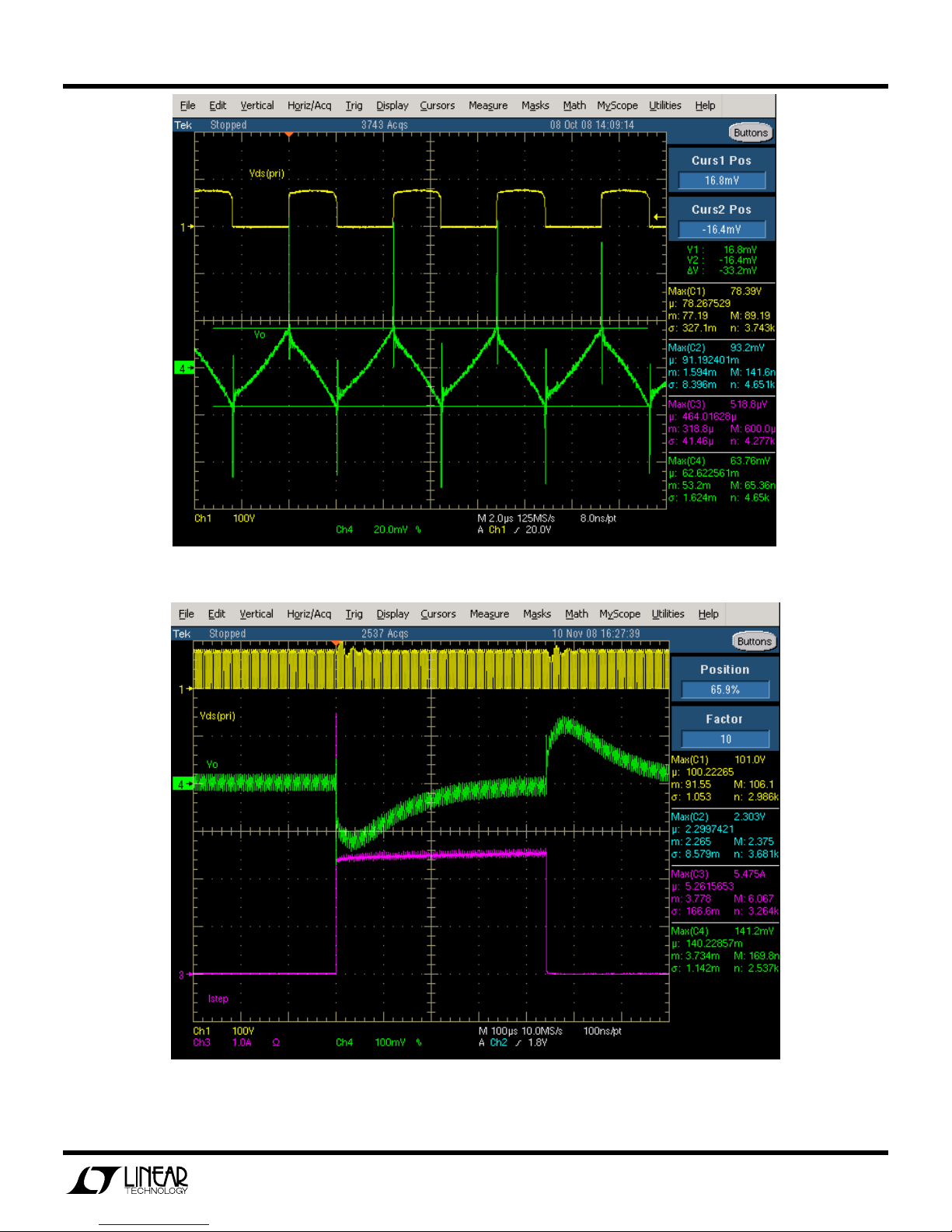
Output Voltage Ripple (37Vport, 5A)
Figure 6.
Load Transient Response (48Vport, 2.5A to 5A to 2.5A)
QUICK START GUIDE FOR DEMONSTRATION CIRCUIT 1351A
SINGLE OUTPUT, HIGH POWER, HIGH EFFICIENCY POE
6
Figure 7.
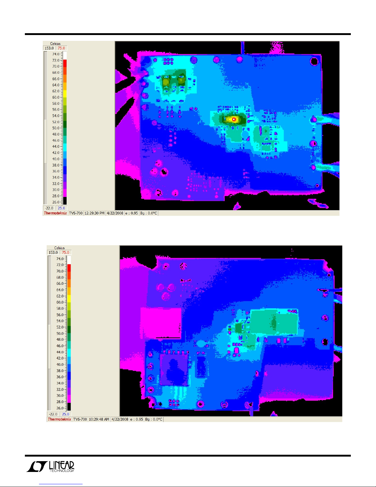
Temp Data (37Vport, 5A, Top)
Figure 8.
Temp Data (37Vport, 5A, Bottom)

QUICK START GUIDE FOR DEMONSTRATION CIRCUIT 1351A
SINGLE OUTPUT, HIGH POWER, HIGH EFFICIENCY POE
7
Figure 9.
Loop Plot (5A out)
Figure 10.
Loop Plot (0A out)

QUICK START GUIDE FOR DEMONSTRATION CIRCUIT 1351A
SINGLE OUTPUT, HIGH POWER, HIGH EFFICIENCY POE
8
Figure 11.
Stresses (57Vport, 5A)
Figure 12.
Stresses (37Vport, 5A)
QUICK START GUIDE FOR DEMONSTRATION CIRCUIT 1351A
SINGLE OUTPUT, HIGH POWER, HIGH EFFICIENCY POE
9
This manual suits for next models
1
Table of contents
Other Linear Power Supply manuals


Popular Power Supply manuals by other brands


Granit
Granit 580580477 operating instructions

Mitsubishi Electric
Mitsubishi Electric 9900D Series Owner technical manual

Altronix
Altronix SMP7 quick start guide

VOLTCRAFT
VOLTCRAFT PA 300 operating instructions

Spondoolies tech
Spondoolies tech SP20 Jackson user guide

Trellix
Trellix NS3 00 Series quick start guide