M13design M13-RA6M3-EK User manual

M13-RA6M3-EK
RA6M3 (Cortex-M4)
Evaluation Kit
USER MANUAL
Board name:
M13-RA6M3-EK
MCU:
R7FA6M3AH3CFC
Updated on the: 16 Dec. 21
Version
1.0.3

M13design - 16 Dec. 21 2/53
TABLE OF CONTENT
1OVERVIEW ...................................................................................................................................... 7
1.1 Introduction .............................................................................................................................. 7
1.2 Features ................................................................................................................................... 8
2HARDWARE LAYOUT AND CONFIGURATION............................................................................ 9
2.1 Hardware block diagram .......................................................................................................... 9
2.2 The M13-RA6M3-EK Board layout ........................................................................................ 10
3M13-RA6M3-EK PIN ASSIGNMENT............................................................................................. 12
3.1 RA6M3 system and Power pins............................................................................................. 12
3.1.1 Boot pin........................................................................................................................ 12
3.1.2 System Reset pin......................................................................................................... 12
3.1.3 Clock source ................................................................................................................ 13
3.1.4 Power supply ............................................................................................................... 14
3.2 External memory .................................................................................................................... 15
3.2.1 Serial Flash Memory .................................................................................................... 15
3.2.2 SDRAM ........................................................................................................................ 16
3.2.3 EEPROM ..................................................................................................................... 17
3.3 4.3-inch TFT LCD Module...................................................................................................... 18
3.4 USB Interface......................................................................................................................... 19
3.5 LAN Interface ......................................................................................................................... 20
3.6 SD/MMC Host Interface (4-bits)............................................................................................. 21
3.7 Audio Interface ....................................................................................................................... 22
3.8 3-Axis Accelerometer ............................................................................................................. 23
3.9 J-Link OB................................................................................................................................ 24
3.10 VGA camera module.............................................................................................................. 26
3.11 I²C Interface ........................................................................................................................... 27
3.12 User Interface: Switch, Led, Potentiometer ........................................................................... 28
4CONNECTOR OVERVIEW............................................................................................................ 29
4.1 CN1: USB-Micro A/B.............................................................................................................. 29
4.2 CN2: USB-Micro A/B.............................................................................................................. 29
4.3 CN4: 19-Pin JTAG Header..................................................................................................... 30
4.4 CN6: RJ45.............................................................................................................................. 31
4.5 CN7: LCD Connector ............................................................................................................. 32
4.6 CN8: LCD Capacitive Touch.................................................................................................. 33
4.7 CN9: 8 Bit VGA Camera module ........................................................................................... 33
4.8 CN10: Micro SD Card ............................................................................................................ 34
4.9 CN11: 4-Pole Audio Jack ....................................................................................................... 35
4.10 CN12: Expansion Connector - mikroBUS .............................................................................. 36
4.11 CN13/CN14: Expansion Connectors – PMOD....................................................................... 37
4.12 CN15: +5VDC Power Jack..................................................................................................... 39

M13design - 16 Dec. 21 3/53
TABLE OF CONTENT (Continued)
5MULTIPLEXED FUNCTIONS........................................................................................................ 40
5.1 SDRAM Selection .................................................................................................................. 41
5.1.1 DATA / SPI0................................................................................................................. 42
5.1.2 ADDR / SSIE0.............................................................................................................. 42
5.1.3 ADDR / SCI2................................................................................................................ 42
5.1.4 ADDR / SCI6................................................................................................................ 43
5.1.5 PMOD2 ........................................................................................................................ 43
5.1.6 “Default” and “SDRAM ready” shunt Configuration recap ........................................... 44
5.2 SD CARD / QSPI ................................................................................................................... 45
5.3 TDI / CTS2 / IRQ11................................................................................................................ 46
5.4 SDA0_B / USB_VBUS ........................................................................................................... 47
6RELATED DOCUMENTS .............................................................................................................. 48
7ORDERING INFORMATION.......................................................................................................... 49
8TECHNOLOGY PARTNERS ......................................................................................................... 50
9REVISION HISTORY ..................................................................................................................... 51

M13design - 16 Dec. 21 4/53
LIST OF TABLES
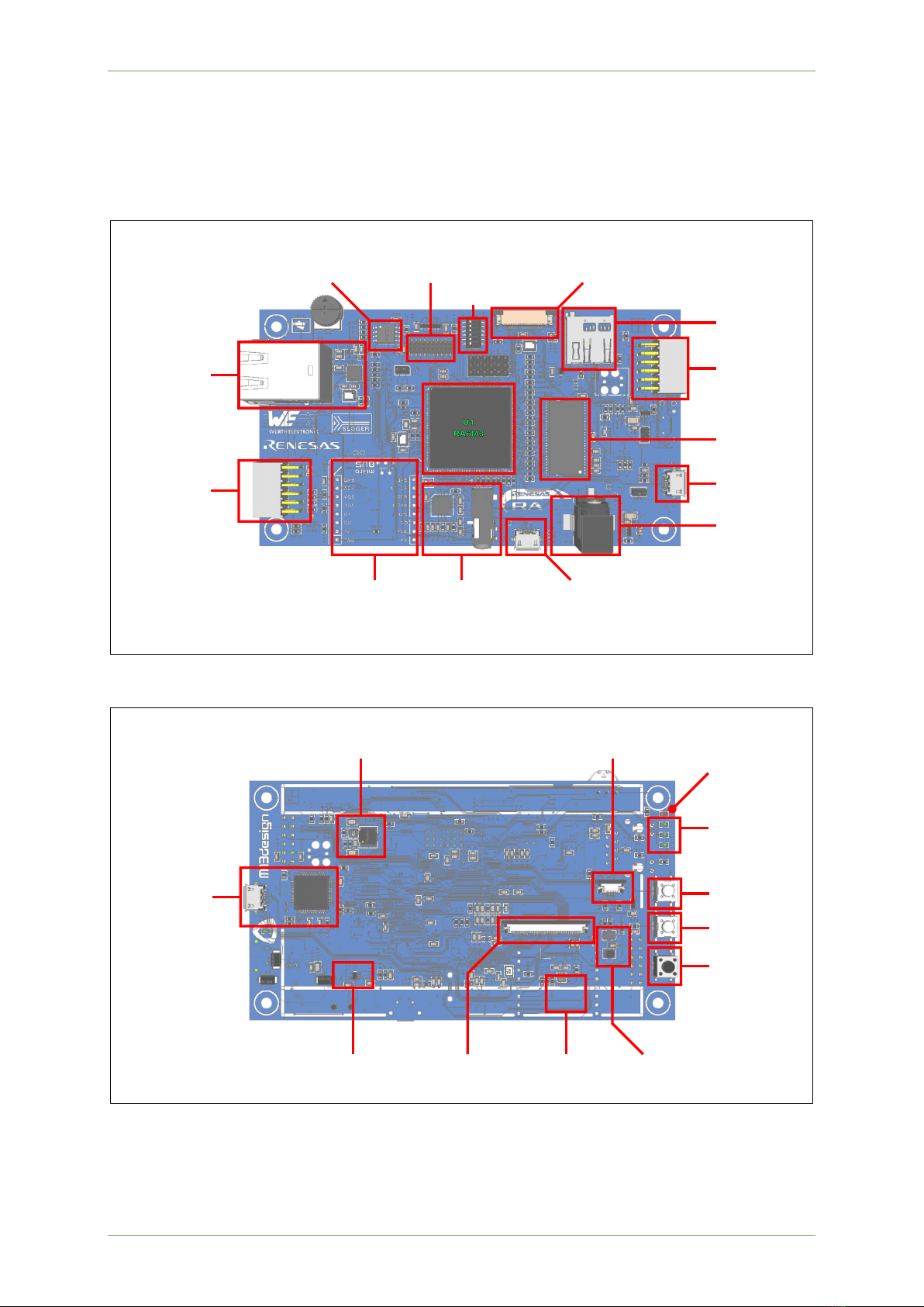
Table 1. Top main component list ......................................................................................................... 11
Table 2. Bottom main component list .................................................................................................... 11
Table 3. Boot pins.................................................................................................................................. 12
Table 4. JP2 .......................................................................................................................................... 12
Table 5. System Reset pin .................................................................................................................... 12
Table 6. Clock Source Assignment ....................................................................................................... 13
Table 7. Serial Flash Memory Overview ............................................................................................... 15
Table 8. Serial Flash Memory Pin Assignment ..................................................................................... 15
Table 9. SDRAM overview .................................................................................................................... 16
Table 10. SDRAM Address Bus Pin Assignment.................................................................................. 16
Table 11. EEPROM Overview............................................................................................................... 17
Table 12. IIC0 Pin assignment .............................................................................................................. 17
Table 13. TFT LCD Module Overview................................................................................................... 18
Table 14. Capacitive Touchscreen........................................................................................................ 18
Table 15. LCD Assignment Pins ........................................................................................................... 18
Table 16. USB Overview ....................................................................................................................... 19
Table 17. USB Pin Assignment ............................................................................................................. 19
Table 18. Ethernet PHY Overview ........................................................................................................ 20
Table 19. Ethernet Assignment Pins ..................................................................................................... 20
Table 20. P706 Multiplexing .................................................................................................................. 20
Table 21. SD/MMC Interface Pin Assignment....................................................................................... 21
Table 22. Audio CODEC Overview ....................................................................................................... 22
Table 23. Audio Pin Assignment ........................................................................................................... 22
Table 24. Accelerometer Overview ....................................................................................................... 23
Table 25. IIC0 Pin assignment .............................................................................................................. 23
Table 26. SWD/JTAG Pin Assignment.................................................................................................. 24
Table 27. Debug Configuration.............................................................................................................. 25
Table 28. VGA Camera Module Overview ............................................................................................ 26
Table 29. 8bit VGA Interface Pin Assignment....................................................................................... 26
Table 30. I²C pin assignment................................................................................................................. 27
Table 31. User Interface Overview........................................................................................................ 28
Table 32. User Interface Pin Assignment.............................................................................................. 28
Table 33. CN1 Pin Description .............................................................................................................. 29
Table 34. CN2 Pin Description .............................................................................................................. 29
Table 35. CN4 Pin Assignment ............................................................................................................. 30
Table 36. CN6 Pin Assignment ............................................................................................................. 31
Table 37. CN7 Pin Assignment ............................................................................................................. 32
Table 38. CN8 Pin Assignment ............................................................................................................. 33
Table 39. CN9 Pin Assignment ............................................................................................................. 33

M13design - 16 Dec. 21 5/53
LIST OF TABLES (Continued)
Table 40. CN10: Micro SD Card Pin Assignment.................................................................................. 34
Table 41. CN11 Pin Assignment ........................................................................................................... 35
Table 42. CN12 Pin Assignment ........................................................................................................... 36
Table 43. mikroBUSTM Overview ........................................................................................................... 36
Table 44. PMOD Connector Overview .................................................................................................. 37
Table 45. CN13 (PMOD1) Pin Assignment........................................................................................... 37
Table 46. CN14 (PMOD2) Pin Assignment........................................................................................... 38
Table 47. CN15 Connector Overview.................................................................................................... 39
Table 48. CN15 Pin Assignment ........................................................................................................... 39
Table 49. Multiplexing Function Table................................................................................................... 40
Table 50. Multiplexing SDRAM Data & SPI0......................................................................................... 42
Table 51. Multiplexing SDRAM Addresses & SSIE0............................................................................. 42
Table 52. Multiplexing SDRAM Addresses & SCI2............................................................................... 42
Table 53. Multiplexing SC6 & SDRAM Addresses................................................................................ 43
Table 54. Multiplexing PMOD_RST & SDRAM Address....................................................................... 43
Table 55. Shunt Configuration............................................................................................................... 44
Table 56. QSPI/SDHI Selection ............................................................................................................ 45
Table 57. Multiplexing TDI / CTS2 / IRQ11........................................................................................... 46
Table 58. Multiplexing SDA0_B & USB_VBUS..................................................................................... 47
Table 59. Ordering Information ............................................................................................................. 49
Table 60. Default/SDRAM-Ready Features .......................................................................................... 49
Table 61. Hardware Technology Partners............................................................................................. 50
Table 62. Software Technology Partners .............................................................................................. 50
Table 63. Revision Table....................................................................................................................... 51

M13design - 16 Dec. 21 6/53
LIST OF FIGURES
Figure 1. M13-RA6M3-EK Component View (Top)................................................................................. 7
Figure 2. M13-RA6M3-EK LCD View (Bottom) ....................................................................................... 7
Figure 3. Bloc Diagram............................................................................................................................ 9
Figure 4. Top main component Layout.................................................................................................. 10
Figure 5. Bottom main component layout (Bottom view) ...................................................................... 10
Figure 6. Reset Block Diagram.............................................................................................................. 12
Figure 7. Clock Source Diagram ........................................................................................................... 13
Figure 8. RA6M3 Power Supply Overview............................................................................................ 14
Figure 9. USB Diagram ......................................................................................................................... 19
Figure 10.SD/MMC Host Interface Diagram.......................................................................................... 21
Figure 11. Audio Block Diagram............................................................................................................ 22
Figure 12. Debug Interface Diagram ..................................................................................................... 24
Figure 13. SW2 Illustration .................................................................................................................... 25
Figure 14. I²C bus diagram.................................................................................................................... 27
Figure 15. User Interface diagram......................................................................................................... 28
Figure 16. CN1: USB-Micro A/B Front view .......................................................................................... 29
Figure 17. CN2: USB- Micro A/B Front view ......................................................................................... 29
Figure 18. CN4: 19-pin JTAG Header ................................................................................................... 30
Figure 19. CN6. RJ45 Bottom View ...................................................................................................... 31
Figure 20. CN7. Front View................................................................................................................... 32
Figure 21. CN8 Front View.................................................................................................................... 33
Figure 22. CN9 Front View.................................................................................................................... 33
Figure 23. CN10: MicroSD Card Bottom View ...................................................................................... 34
Figure 24. CN11 Mating Plug and Bottom View.................................................................................... 35
Figure 25. CN12 mikroBUSTM Top view ................................................................................................ 36
Figure 26. PMOD Front View ................................................................................................................ 37
Figure 27. CN15 Power Jack................................................................................................................. 39
Figure 28. Shunt Footprint..................................................................................................................... 40
Figure 29. Shunt general location ......................................................................................................... 41
Figure 30. JP3 to JP8 Top location ....................................................................................................... 45

M13-RA6M3-EK_UM - Rev1.0.2 Overview
M13design - 16 Dec. 21 7/53
1 OVERVIEW
1.1 INTRODUCTION
The M13-RA6M3-EK is complete evaluation and development platform for the Renesas Electronics®
32-bit Microcontroller RA family Cortex®-M4 based R7FA6M3AH3CFC microcontroller. The full range of
the hardware features on the board helps users to quickly evaluate all the available peripherals (10/100-
Mbit Ethernet, microSDTM card, USB HS/FS, Audio codec with 4-pole Jack, SDRAM, Quad-SPI Flash
memory,4.3-inch colour LCD-TFT with capacitive touch panel, and many others) and to develop their
custom applications. PMODTM and MikrobusTM connectors make it possible to easily extent the board’s
features (Sensors, communication and network modules and many more). The integrated JLink-OB
debug probe provides in-circuit debug and programming for the RA6M3 device and also a built-in VCOM
functionality.
Figure 1. M13-RA6M3-EK Component View (Top)
Figure 2. M13-RA6M3-EK LCD View (Bottom)

M13-RA6M3-EK_UM - Rev1.0.2 Overview
M13design - 16 Dec. 21 8/53
1.2 FEATURES
•Renesas RA6M3 (Cortex®-M4) Microcontroller R7FA6M3AH3CFC
•LQFP176 Package
•2Mbyte Internal Flash
•640Kbyte Internal RAM
•32Mbyte external SDRAM (Multiplexed)
•32Mbyte external Serial Flash
•16Kbit I²C EEPROM
•4.3-inch 480x272 TFT LCD with capacitive touch panel
•USB Interface
•LAN Interface
•SD/MMC Host Interface (4 bits)
•I2S Audio codec
•3-Axis accelerometer
•On-board JLINK-OB debugger with VCOM
•19-pins 1.27mm pitch JTAG connector
•Board connectors
1 x 8-bit Interface camera
1 x Ethernet RJ45
2 x USB Micro-AB
1 x USB Micro-AB for debugger
1 x microSDTM card
1 x MikrobusTM
2 x PMOD
1 x 4-pole 3.5mm Jack
1 x 2.1mm 5V Power Jack
•2 x User switch and 1 x Reset switch
•1 x Mono-turn 10KΩ Potentiometer
•3 x User LEDs
•1 x Power-on LED

M13-RA6M3-EK_UM - Rev1.0.2 Hardware layout and configuration
M13design - 16 Dec. 21 9/53
2 HARDWARE LAYOUT AND CONFIGURATION
2.1 HARDWARE BLOCK DIAGRAM
Figure 3. Bloc Diagram
UART
JTAG
HEADER
RA6M3
TQFP176
JLINK-OB 24MHz EXTAL
RGB888
RIIC
4.3-inch
TFT Module
480x272px
CAP TOUCH
PANEL
ETH PHY RJ45RMII
USB
Micro-AB
RGB8Bit
RTC32KHz
FLASH SPIBSC
SDIO
SDRAM ADDR/DATA/CTL
EEPROM RIIC
MODE SEL.
JP2 P201
USBHS
(HOST/DEVICE)
USBFS
(HOST/DEVICE)
USB
CAMERA
Connector
RIIC 3-Axis
MEMS
USER
SW/LED
GPIOS
RST RESET
SW
RESET
Monitor IC
RST from
JLINK-OB
JTAG
MIKROBUS
SPI/UART
IRQ/GPIOs
PMOD X 2
SPI
IRQ/GPIOs
Audio
Codec
SSIF-2 / RIIC 4-Pole
3.5mm Jack
5V
2.1mm
JACK
DC/DC 1V8
DC/DC 3V3
POWER
JLINK-OB

M13-RA6M3-EK_UM - Rev1.0.2 Hardware layout and configuration
M13design - 16 Dec. 21 10/53
2.2 THE M13-RA6M3-EK BOARD LAYOUT
Figure 4 and Figure 5 Show the layout of the main components of the board.
Figure 4. Top main component Layout
Figure 5. Bottom main component layout (Bottom view)
C6: RJ45 Connector
U7: Ethernet PHY
CN13: PMOD LEFT
CN14: PMOD RIGHT
CN1: USBFS
U9: SDRAM
CN15: PWR JACK
CN2: USBHSU11: AUDIO CODEC
CN11: 4-POLE AUDIO JACK
CN12: MIKROBUS
CN10: uSD CARD
CN9: CAMERA
SW2
CN4: JTAG 19PINSU8: SERIAL FLASH
CN5/U6: JLINK-OB
D1/D2/D3: USER LEDS
U12: ACCELEROMETER
U14: 5V TO 3V3 DC/DC
U15: 5V TO 1V8 DC/DC
SW2: USER SWITCH
SW1: USER SWITCH
SW3: RESET
CN7: LCD CONNECTOR U13: LCD BACKLIGHT
CN8: CAPACITIVE TOUCH
D8: PWR LED

M13-RA6M3-EK_UM - Rev1.0.2 Hardware layout and configuration
M13design - 16 Dec. 21 11/53
Table 1And Table 2list the main component mounted on the M13-RA6M3-EK board
Table 1. Top main component list
Component
Reference Description MFR1 / MPN2NOTES
U1
CPU
Renesas / R7FA6M3AH3CFC
U7
Ethernet PHY
Microchip / KSZ8081RNA
U8
Serial Flash Memory
Macronix / MX25L25645GM2I-08G
U9
SDRAM
Winbond / W9825G6KH-6I
U11
Audio Codec
Maxim / MAX9867ETJ
CN1
USB FS
Würth Electronics / 629105150921
Mini USB-AB
CN2
USB HS
Würth Electronics / 629105150921
Mini USB-AB
CN4
19pins JTAG connector
Würth Electronics / 62102021021
1.27mm Pitch
CN6
RJ45 connector
Würth Electronics / 7499011121A
CN9
Camera connector
Würth Electronics / 68712414022
Top contact
CN10
Micro SD Card
Würth Electronics / 693071010811
CN11
4-pole Jack headphone
Cui Inc. / SJ-43514-SMT-TR
3.5mm
CN12 mikroBUSTM Würth Electronics / 61300811821
CN12.1 & CN12.2 in the
BOM
CN13
PMOD1
Würth Electronics / 613012243121
CN14
PMOD2
Würth Electronics / 613012243121
CN15
5V, 2.1mm, Power Jack
Würth Electronics / 694106105102
Strictly 5VDC
SW2
JLink-OB Disconnection
Omron / A6H-6101
Table 2. Bottom main component list
Component
Reference Description MFR1 / MPN2NOTES
U6
JLink-OB
Segger
U12
3-Axis Accelerometer
Würth Electronics / 2533020201601
U13
LCD Backlight
Renesas / ISL97634IRT26Z-T
U14
3V3 DC/DC regulator
Renesas / ISL80030AFRZ-T7A
U15
1V8 DC/DC regulator
Renesas / ISL9008AIECZ-T
CN5
JLink-OB connector
Würth Electronics / 629105150921
Mini USB-AB
CN7
LCD connector
Würth Electronics / 687140183722
Bottom contact
CN8
Capacitive Touch
connector
Würth Electronics / 687106183722
D1/D2/D3
User Leds
Würth Electronics / 150060VS55040
Green Led
D8
Power Led
Würth Electronics / 150060RS55040
Red Led
SW1
Reset Switch
C&K / PTS645SL43SMTR92LFS
Black coloured
SW3/SW4
User Switches
C&K / PTS645SM43SMTR92LFS
Blue coloured
Note 1: Manufacturer name
Note 2: Manufacturer Part Number

User Manual - Rev1.0.2 M13-RA6M3-EK pin assignment
M13design - 16 Dec. 21 12/53
3 M13-RA6M3-EK PIN ASSIGNMENT
3.1 RA6M3 SYSTEM AND POWER PINS
3.1.1 BOOT PIN
Table 3. Boot pins
U1 Pin Pin Functions
Board
Assignment
Signal Name
Default
Function
Remarks
68
P201/MD
MD
N/A
System
By default, the board is in Single-Chip mode (JP2 left open). In order to switch to SCI/USB boot mode,
connect JP2 with a 2mm jumper as stated in Table 4.
Table 4. JP2
U1 Pin Pin Functions JP2 Pin status Operating Mode
68
P201/MD
Opened
Pulled-up
Single-chip mode
68
P201/MD
Closed
Pulled-down
SCI/USB boot mode
3.1.2 SYSTEM RESET PIN
Table 5. System Reset pin
U1 Pin Pin Functions
Board
Assignment
Signal Name
Default
Function
Remarks
67
RESET#
Reset
nRESET_SYS
System
The M13-RA6M3-EK System Reset signal is controlled by 3 sources: The power-on reset with the
Voltage supervisor U4, the Reset Switch (SW1) and the JTAG reset signal. Figure 6shows the reset
block diagram.
Figure 6. Reset Block Diagram
As illustrated in Figure 6, the board’s Reset signal is also directly connected to the Reset signal of the
Ethernet PHY (U7) and the Capacitive Touch driver (CN8). This is done to compensate the lack of free
GPIOs left after mapping all the dedicated peripheral of the board.
RESET#
RA6M3
67
RST#
U7 (ETHERNET PHY)
24
RST
CN8 (CAP TOUCH)
4
A
BGND
VCC
Y
1
2
3 5
4
U5
SN74LVC1G08DBVR
R17 10K
3V3D
3V3D
C44 100nF
3V3D
C46 100nF
nRESET
R18 10K
3V3D
/RST
VCC
VSS
2
31
U4
ISL88002IH29Z-TK
3 1
24
SW3
PTS645SL43SMTR92LFS
SW_RESET
nRESET_SYS

User Manual - Rev1.0.2 M13-RA6M3-EK pin assignment
M13design - 16 Dec. 21 13/53
3.1.3 CLOCK SOURCE
The M13-RA6M3-EK has 2 clock input sources as shown in Figure 7and Table 6gives you the
connections for each clock on the RA6M3.
- Main clock : 24MHz crystal
- RTC clock : 32.768KHz crystal
Table 6. Clock Source Assignment
U1 Pin RA6M3 Pin Functions
Board Function
Assignment
Signal Name
Default
Function
Remarks
24
EXTAL/P212
Main clock
EXTAL
Clock
23
XTAL/P213
Main clock
XTAL
Clock
20
XCIN
RTC clock
XCIN
Clock
21
XCOUT
RTC clock
XCOUT
Clock
Figure 7. Clock Source Diagram
EXTAL / P212
RA6M3
24
23
20
21
XTAL / P213
XCIN
XCOUT
C89.0pF
C99.0pF
C1018pF
C1118pF
R11
1M
R10
3K3
1
2
4
3
X2
24Mhz
21
X1
32.678KHz

User Manual - Rev1.0.2 M13-RA6M3-EK pin assignment
M13design - 16 Dec. 21 14/53
3.1.4 POWER SUPPLY
The M13-RA6M3-EK has 2 sources for its power supply. The Primary source is from the +5VDC/500mA
of the J-Link OB USB connector CN5 as shown in Figure 8. The Secondary source is provided through
the 2.10mm Power Jack connector CN15 and is strictly limited to a +5VDC power supply. Even though
the power source is protected by diodes (D5 and D6) be extra cautious as to not provide the board’s
power from the Primary and the Secondary sources simultaneously.
Figure 8. RA6M3 Power Supply Overview
Two DC/DC regulators are used to generate all the required power rails needed on the board. The 1V8
rail is exclusively used by the Audio Codec as shown by the Figure 8.
RA6M3
CN5
CN15
5V to 1V8
AVCC0
J-LINK OB
POWER JACK
5V to 3V3
VREFH
VREFH0
VCC
VBAT
VCC_USB
VCC_USBHS
AVCC_USBHS
AUDIO CODEC
AVDD
PVDD
1V8D
3V3D
26
5
32
23
26
34
48
18
24...171
158
154
155
D5
PMEG3020EP
D6
PMEG3020EP
5V_IN
AVCC03V3D
1V8D

User Manual - Rev1.0.2 M13-RA6M3-EK pin assignment
M13design - 16 Dec. 21 15/53
3.2 EXTERNAL MEMORY
3.2.1 SERIAL FLASH MEMORY
The M13-RA6M3-EK board is equipped with a serial flash memory which is controlled by RA6M3 on-
chip Quad Serial Peripheral Interface (QSPI). By default, the Serial Flash Memory is connected to the
MCU but it can be switched to SD Card anytime. Table 7Shows the serial Flash Memory Overview.
Table 7. Serial Flash Memory Overview
Device Type MFR1/ MPN2Operational Voltage
Capacity
Package
Serial Flash
Macronix /
MX25L25645GM2I-
08G
3.3V 32Mbyte 8-SOP (200mil)
Note 1: Manufacturer name
Note 2: Manufacturer Part Number
Table 8Shows the pin assignment between the RA6M3 CPU (U1) and the Serial Flash Memory (U8).
Table 8. Serial Flash Memory Pin Assignment
U1 Pin RA6M3 Pin Functions
Board
Assignment
Signal Name
Default
Function
Remarks
140
P500
JP3
QSPCLK
QSPI
Multiplexed
141
P501
JP4
QSSL
QSPI
Multiplexed
142
P502
JP5
QIO0
QSPI
Multiplexed
143
P503
JP6
QIO1
QSPI
Multiplexed
144
P504
JP7
QIO2
QSPI
Multiplexed
145
P505
JP8
QIO3
QSPI
Multiplexed
The Serial Flash Memory device is connected to the RA6M3 through the JP3-JP8 jumpers. See Section
5.2 SD CARD for detailed information on multiplexing the P500-P505 signals.

User Manual - Rev1.0.2 M13-RA6M3-EK pin assignment
M13design - 16 Dec. 21 16/53
3.2.2 SDRAM
The M13-RA6M3-EK is also equipped with an external 16 bits SDRAM. This memory device is
controlled by the RA6M3 Bus State Controller. Table 9shows the SDRAM Memory Overview while
Table 10 shows the pin assignment between the RA6M3 and the SDRAM device.
Table 9. SDRAM overview
Device Type MFR1/ MPN2Operational Voltage
Capacity
Package
SDRAM
Winbond /
W9825G6KH-6I
3.3V 32Mbyte TSOP54
Note 1: Manufacturer name
Note 2: Manufacturer Part Number
Table 10. SDRAM Address Bus Pin Assignment
U1 Pin RA6M3 Pin Functions
Board
Assignment
Signal Name
Default
Function
Remarks
96
P115 / SSITXD0_B / A01
Multiplexed
A1
SSIE0
95
P114 / SSIRXD0_B / A02
Multiplexed
A2
SSIE0
94
P113 / SSILRCK0 / A03
Multiplexed
A3
SSIE0
93
P112 / SSIBCK0_B / A04
Multiplexed
A4
SSIE0
92
P111 / IRQ4 / A05
Multiplexed
A5
PMOD2
87
P301 / RXD2 / A06
Multiplexed
A6
MIKROBUS
86
P302 / TXD2 / A07
Multiplexed
A7
MIKROBUS
85
P303 / A08
SDRAM
A8
SDRAM
82
P304 / SCL6 / A09
Multiplexed
A9
SCI6
81
P305 / SD6 / A10
Multiplexed
A10
SCI6
80
P306 / A11
SDRAM
A11
SDRAM
79
P307 / A12
SDRAM
A12
SDRAM
78
P308 / A13
SDRAM
A13
SDRAM
77
P309 / A14
SDRAM
A14
SDRAM
76
P310 / A15
SDRAM
A15
SDRAM
132
P100 / MISOA_A / DQ0
Multiplexed
DQ0
SPI
131
P101 / MOSIA_A / DQ1
Multiplexed
DQ1
SPI
130
P102 / RSPCKA_A / DQ2
Multiplexed
DQ2
SPI
129
P103 / SSLA0_A / DQ3
SDRAM
DQ3
SDRAM
128
P104 / SSLA1_A / DQ4
Multiplexed
DQ4
PMOD1
127
P105 / SSLA2_A / DQ5
Multiplexed
DQ5
PMOD2
126
P106 / SSLA3_A / DQ6
SDRAM
DQ6
SDRAM
125
P107 / DQ7
SDRAM
DQ7
SDRAM
103
P612 / DQ8
SDRAM
DQ8
SDRAM
104
P613 / DQ9
SDRAM
DQ9
SDRAM
105
P614 / DQ10
SDRAM
DQ10
SDRAM
117
P605 / DQ11
SDRAM
DQ11
SDRAM
118
P604 / DQ12
SDRAM
DQ12
SDRAM
119
P603 / DQ13
SDRAM
DQ13
SDRAM
133
P800 / DQ14
SDRAM
DQ14
SDRAM
134
P801 / DQ15
SDRAM
DQ15
SDRAM
100
P609 / CKE
SDRAM
CKE
SDRAM
99
P608 / A0 / DQM1
SDRAM
A00/DQM1
SDRAM
UDQM
121
P601 / DQM0
Multiplexed
DQM0
PMOD2
LDQM
75
P311 / RAS
SDRAM
RAS#
SDRAM
102
P611 / SDCS#
SDRAM
SDCS#
SDRAM
74
P312 / CAS
SDRAM
CAS#
SDRAM
101
P610 / WE
SDRAM
WE#
SDRAM
As detailed in the Table 10, the SDRAM device U9 is by default not connected to the RA6M3 MCU even
though it is included on the board. Check section 5.1 SDRAM Selection to see how the SDRAM can be
selected.

User Manual - Rev1.0.2 M13-RA6M3-EK pin assignment
M13design - 16 Dec. 21 17/53
3.2.3 EEPROM
An EEPROM is also available on the M13-RA6M3-EK board. This memory device is controlled by the
RA6M3 I²C Interface on channel 0 (IIC0) which is the board’s main I²C bus. Table 11 shows the
EEPROM Memory Overview. See section 3.11 I²C Interface to have a full illustration on what I²C devices
are available on the board.
Table 11. EEPROM Overview
Device Type MFR1/ MPN2I²C Address
Capacity
Package
EEPROM
On Semiconductor /
CAT24AA16TDI-GT3
W: 1010 0000 (0xA0)
R: 1010 0001 (0xA1)
2048x8 bits
(16Kbits)
TSOT-23-5
Table 12. IIC0 Pin assignment
U1 Pin RA6M3 Pin Functions
Board
Assignment
Signal Name
Default
Function
Remarks
52
P204 / SCL0_B
Main I²C bus
SCL0
IIC0
44
P407 / SDA0_B
Multiplexed
SDA0
IIC0

User Manual - Rev1.0.2 M13-RA6M3-EK pin assignment
M13design - 16 Dec. 21 18/53
3.3 4.3-INCH TFT LCD MODULE
The 4.3-Inch TFT LCD module included in this kit is connected and controlled by the Graphics LCD
Controller which by default will output the video image in RGB565 format even though the LCD module
is mapped on the complete RGB888 bus. This module comes with a Capacitive touchscreen as shown
in Table 13 which is accessible by the SCI6 bus. As for Table 15, it shows the pin assignment between
the RA6M3 and the TFT module.
Table 13. TFT LCD Module Overview
Device Type MFR1/ MPN2
Diagonal
Size
Display
Format
Package
TFT LCD Module
EastRising /ER-TFT043-3
4.3-Inch 480x272px N/A
Table 14. Capacitive Touchscreen
Device Type MFR1/ MPN2
Diagonal
Size
I²C Address Package
Capacitive
Touchscreen
EastRising / ER-TPC043-2
4.3-Inch W: 0111 0000 (0x70)
R: 0111 0001 (0x71) N/A
Table 15. LCD Assignment Pins
U1 Pin RA6M3 Pin Functions
Board
Assignment
Signal Name
Default
Function
ER-TFT043-7
signal
137
P804 / LCD_DATA00_B
LCD
LCD_DATA00_B
LCD
R0
136
P803 / LCD_DATA01_B
LCD
LCD_DATA01_B
LCD
R1
135
P802 / LCD_DATA02_B
LCD
LCD_DATA02_B
LCD
R2
116
P606 / LCD_DATA03_B
LCD
LCD_DATA03_B
LCD
R3
115
P607 / LCD_DATA04_B
LCD
LCD_DATA04_B
LCD
R4
114
PA00 / LCD_DATA05_B
LCD
LCD_DATA05_B
LCD
R5
113
PA01 / LCD_DATA06_B
LCD
LCD_DATA06_B
LCD
R6
109
PA10 / LCD_DATA07_B
LCD
LCD_DATA07_B
LCD
R7
108
PA09 / LCD_DATA08_B
LCD
LCD_DATA08_B
LCD
G0
107
PA08 / LCD_DATA09_B
LCD
LCD_DATA09_B
LCD
G1
106
P615 / LCD_DATA10_B
LCD
LCD_DATA10_B
LCD
G2
73
P905 / LCD_DATA11_B
LCD
LCD_DATA11_B
LCD
G3
72
P906 / LCD_DATA12_B
LCD
LCD_DATA12_B
LCD
G4
71
P907 / LCD_DATA13_B
LCD
LCD_DATA13_B
LCD
G5
70
P908 / LCD_DATA14_B
LCD
LCD_DATA14_B
LCD
G6
59
P901 / LCD_DATA15_B
LCD
LCD_DATA15_B
LCD
G7
174
P513 / LCD_DATA16_B
LCD
LCD_DATA16_B
LCD
B0
173
P805 / LCD_DATA17_B
LCD
LCD_DATA17_B
LCD
B1
66
P208 / LCD_DATA18_B
LCD
LCD_DATA18_B
LCD
B2
65
P209 / LCD_DATA19_B
LCD
LCD_DATA19_B
LCD
B3
64
P210 / LCD_DATA20_B
LCD
LCD_DATA20_B
LCD
B4
63
P211 / LCD_DATA21_B
LCD
LCD_DATA21_B
LCD
B5
62
P214 / LCD_DATA22_B
LCD
LCD_DATA22_B
LCD
B6
49
P207 / LCD_DATA23_B
LCD
LCD_DATA23_B
LCD
B7
57
P315 / LCD_DISP
LCD
LCD_DISP3
I/O port
DISP
56
P314 / LCD_TCON1_B
LCD
LCD_TCON1_B
LCD
HSYNC
55
P313 / LCD_TCON2_B
LCD
LCD_TCON2_B
LCD
VSYNC
54
P202 / LCD_TCON3_B
LCD
LCD_TCON3_B
LCD
DE4
58
P900 / LCD_CLK_B
LCD
LCD_CLK_B
LCD
PLCK
Note 1: Manufacturer name
Note 2: Manufacturer Part Number
Note 3: Connected to the LCD Display signal and configured as a general GPIO in output mode with an On/Off behaviour.
Note 4: Data Enable
The LCD signal inputs are assigned in RGB888 format and connected onto the RA6M3 in BGR, little Indian arrangement.

User Manual - Rev1.0.2 M13-RA6M3-EK pin assignment
M13design - 16 Dec. 21 19/53
3.4 USB INTERFACE
The two USB modules, USBFS (Full-Speed) and USBHS, (High-Speed) from the RA6M3 are being
used on this board. Either of them can be used as a USB HOST or a USB DEVICE port, thus Micro A/B
connectors type are being used for each module.
When the USBFS or the USBHS are being used in Host mode, respectively, JP9 or JP1 must be
connected. On the other hand, leave each of them opened if you want each module to function as a
USB device mode. Figure 9illustrates the USB Interface general diagram while Table 17 gives you the
RA6M3 pin assignments. As we lacked the available pins, OTG functions are not mapped nor used.
Figure 9. USB Diagram
Table 16. USB Overview
Device Type MFR1/ MPN2
Package
Note
USB Micro A/B
Würth Electronics / 629105150921
SMD3, Right Angle
CN1
USB Micro A/B
Würth Electronics / 629105150921
SMD3, Right Angle
CN2
Table 17. USB Pin Assignment
U1 Pin RA6M3 Pin Functions
Board
Assignment
Signal Name
Default
Function
Note
44
P407 / USB_VBUS
Multiplexed
USBFS_VBUS_MES
IIC0
46
USB_DM
USB
USBFS_DM
USBFS
47
USB_DP
USB
USBFS_DP
USBFS
151
P014 / AN005 / AN105
USB
USBFS_VBUSEN4
I/O port4
17
PB01 / USBHS_VBUS
USB
USBHS_VBUS
USBHS
31
USBHS_DM
USB
USBHS_DM
USBHS
32
USBHS_DP
USB
USBHS_DP
USBHS
16
PB00 / USBHS_VBUSEN
USB
USBHS_VBUSEN
USBHS
15
P707 /
USBHS_OVRCURA
USB USBHS_OVRCURA USBHS
27
USBHS_RREF
USB
USBHS_RREF
USBHS
Note 1: Manufacturer name
Note 2: Manufacturer Part Number
Note 3: Surface Mount Device
Note 4: As the VBUSEN pin for the USBFS module is not available due to being used by other peripherals, P014 is configurated as a GPIO to ensure the said function.
USB MICRO A/B
HOST/DEVICE
USB MICRO A/B
HOST/DEVICE
USBFS_VBUSEN
R1 2K2
C5 100uF_10V
R3 1K
C6 100uF_10V
R2 2K2
VBUS
D-
D+
ID
SHLD
SHLD
SHLD
SHLD
GNDSHLD
SHLD
1
2
3
4
5
6
7
8
9
10
11
CN2
629105150921
R4 1K8
USBHS_VBUSEN
USBHS_DM
USBHS_DP
USBHS_RREF
P707 /
PB00 /
PB01 /
USBHS_OVRCURA
USBHS_VBUSEN
USBHS_VBUS
XCIN
XCOUT
/ P108
/ P300
/ P109
/ P110
SWDIO / TMS
TCK / SWCLK
SWO / TDO
TDI
EXTAL / P212
XTAL / P213
USB_DM
USB_DP
RESET#
NMI / P200
MD / P201
17
31
32
16
15
27 21
20
89
88
90
91
24
23
47
46
69
67
68
U1
R7FA6M3AH3CFC
C1
10uF_16V
C2
10uF_16V
C7
10uF_16V
C3 100nF
C4 100nF
R6 2K2
R5 10K
IN
EN
OUT
/FLAG
GND
5
4
1
3
2
NCP380HSN05AAT1G
U2
IN
EN
OUT
/FLAG
GND
5
4
1
3
2
NCP380HSN05AAT1G
U3
12
JP1
USBHS_VBUSEN
5V_IN
USBHS_VBUS
5V_IN
3V3D
USB_VBUS
USBHS_OVCR
USBHS_OVCR
R89 1K
R90 1K8
C117 10uF_16V
USB_VBUS_MES
VBUS
D-
D+
ID
SHLD
SHLD
SHLD
SHLD
GNDSHLD
SHLD
1
2
3
4
5
6
7
8
9
10
11
CN1
629105150921
12
JP9
USBFS_DM
USBFS_DP
USBHS_DP
USBFS_VBUSEN
USBHS_DM
USBHS_VBUSEN

User Manual - Rev1.0.2 M13-RA6M3-EK pin assignment
M13design - 16 Dec. 21 20/53
3.5 LAN INTERFACE
The M13-RA6M3-EK embarks an Ethernet PHY (U7) which communicate through the RA6M3 on-chip
ethernet controller ETHERC by using the RMII Interface. The details of this device can be seen in
Table 18. As for the RMII pin assignment they are displayed in Table 19.
Table 18. Ethernet PHY Overview
Device Type MFR1/ MPN2Operational Voltage Bit Rate Package
Ethernet PHY
Microchip / KSZ8081RNA
3.3V 10 Mbps / 100 Mbps N/A
RJ45 Connector
Wurth Elektronik /
7499011121A
N/A N/A Through-Hole
Note 1: Manufacturer name
Note 2: Manufacturer Part Number
Table 19. Ethernet Assignment Pins
U1 Pin RA6M3 Pin Functions
Board
Assignment
Signal Name
Default
Function
Remarks
14
P706 / IRQ7
Multiplexed
ET0_ IRQ7
SD1CD
36
P415 / RMII0_TXDEN_A
Ethernet
RMII0_TXDEN_A
ETHERC (RMII)
37
P414 / RMII0_TXD1_A
Ethernet
RMII0_TXD1_A
ETHERC (RMII)
38
P413 / RMII0_TXD0_A
Ethernet
RMII0_TXD0_A
ETHERC (RMII)
42
P409 / RMII0_RX_ER_A
Ethernet
RMII0_RX_ER_A
ETHERC (RMII)
43
P408 / RMII0_CRS_DV_A
Ethernet
RMII0_CRS_DV_A
ETHERC (RMII)
39
P412 / REF50_CK0_A
Ethernet
REF50_CK0_A
ETHERC (RMII)
41
P410 / RMII0_RXD1_A
Ethernet
RMII0_RXD1_A
ETHERC (RMII)
40
P411 / RMII0_RXD0_A
Ethernet
RMII0_RXD0_A
ETHERC (RMII)
2
P401 / ET0_MDC
Ethernet
ET0_MDC
ETHERC (RMII)
3
P402 / ET0_MDIO
Ethernet
ET0_MDIO
ETHERC (RMII)
172
P806
Ethernet
ET0_LED2
I/O port
P806 is configurated as a standard output to drive the second led available on the RJ45 connector CN6
through its pin LED2-. And as described in table 18, P706 is by default not connected to the Ethernet
PHY IRQ signal (Pin U7.18) but rather to the SD Card “Card Detection” pin (CN10.9). Follow Table 20
if you need interrupt capabilities on your Ethernet Interface.
Table 20. P706 Multiplexing
RA6M3
Pin
RA6M3
Pin Description
Selected
Function SH41 SH42
14 P706 / SD1CD / IRQ7
ET0_IRQ7
Not Fitted
Fitted
SD1CD (Default)
Fitted
Not Fitted
This manual suits for next models
3
Table of contents