Matrix Orbital MOP-TFT480272-43A-BLM-CTB User manual

MOP-TFT480272-43A-BLM-CTB
Hardware Manual
Revision 1.0

MOP-TFT480272-43A-BLM-CTB 2
Contents
Revision History..............................................................................................................................................................................1
Contents .........................................................................................................................................................................................2
1 General Information ....................................................................................................................................................................3
2 Absolute Maximum Ratings.........................................................................................................................................................3
3 Electrical Characteristics..............................................................................................................................................................3
4 Backlight Characteristics..............................................................................................................................................................3
5 Touch Panel Characteristics .........................................................................................................................................................4
6 External Dimensions....................................................................................................................................................................5
7 Electro-Optical Characteristics ....................................................................................................................................................6
8 Interface Description ...................................................................................................................................................................7
8.1 LCM Interface Description ................................................................................................................................................7
8.2 CTB Interface Description .................................................................................................................................................7
9 AC Characteristics ........................................................................................................................................................................8
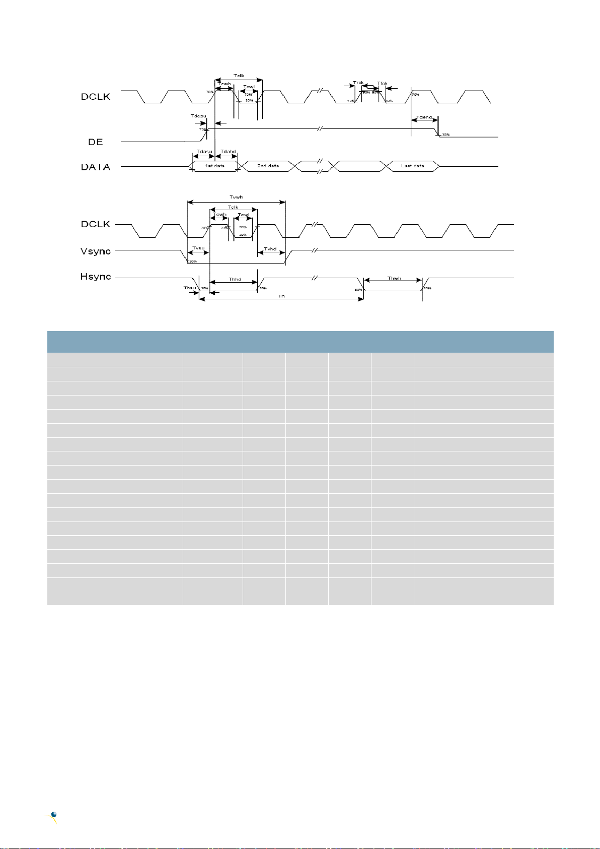
9.1 Pixel Timing.......................................................................................................................................................................8
9.2 Data Timing.......................................................................................................................................................................9
9.3 Touch Panel Timing...........................................................................................................................................................9
10 Power Sequence ......................................................................................................................................................................10
10.1 Power Up Sequence .....................................................................................................................................................10
10.2 Power Down Sequence.................................................................................................................................................10
11 Inspection Criterion .................................................................................................................................................................11
11.1 Description ...................................................................................................................................................................11
11.2 Sample plan ..................................................................................................................................................................11
11.3 Inspection condition.....................................................................................................................................................11
11.4 Definition of inspection zone in LCD.............................................................................................................................11
11.5 Function Defect ............................................................................................................................................................11
11.6 LCD pixel defect ............................................................................................................................................................12
11.7 Dot and line defect .......................................................................................................................................................12
12 Handling Precautions...............................................................................................................................................................13
12.1
Mounting method
.....................................................................................................................................................13
12.2
LCD Handling and Cleaning Precaution
..................................................................................................................13
12.3 Static Charge Precaution ..............................................................................................................................................13
12.4 Packing
........................................................................................................................................................................13
12.5 Precautions during Operation
.................................................................................................................................13
12.6 Storage Recommendations
.....................................................................................................................................14
12.7 Safety Precautions
....................................................................................................................................................14
13 Ordering ..................................................................................................................................................................................15
13.1 Part Numbering Scheme...............................................................................................................................................15
13.2 Options .........................................................................................................................................................................15
14 Contact ....................................................................................................................................................................................15

3MOP-TFT480272-43A-BLM-CTB
1General Information
No.
Item
Contents
Unit
1
LCD size
4.3 inch (Diagonal)
/
2
LCD type
TN/Normally white/Transmissive
/
3
Viewing direction
12 O’clock
/
4
Gray scale inversion direction
6 O’clock
/
5
Resolution
480 *272 Pixels
/
6
Module size (W* H*T)
105.5*67.2*4.85
mm
7
Active area (W*H)
95.04*53.856
mm
8
Pixel pitch (W*H)
0.198*0.198
mm
9
Interface Type
RGB interface
/
10
Module power consumption
0.0792(Without backlight)
W
11
Back light Type
LED
/
12
Driver IC
ILI6480BQ or compatible
/
13
Weight
69
g
2Absolute Maximum Ratings
Item
Symbol
Min
Max
Unit
Power supply voltage(LCD Module)
VDD
-0.5
5
V
Back-light current (normal temp.)
ILED
-
50
mA
Operation temperature
Top
-20
70
°C
Storage temperature
Tst
-30
80
°C
Humidity
RH
-
90%(Max60 °C)
RH
3Electrical Characteristics
DC Characteristics (at Ta=25°C)
Item
Symbol
Min
Typ
Max
Unit
Power Supply Input Voltage
VDD
3.0
3.3
3.6
V
I/O logic voltage
VDDIO
1.8
-
3.3
V
Input voltage 'H' level
VIH
0.7VDD
-
VDD
V
Input voltage 'L' level
VIL
VSS
-
0.3VDD
V
Power Supply Current
IVDD
-
24
-
mA
TFT gate on voltage
VGH
-
N/A
-
V
TFT gate off voltage
VGL
-
N/A
-
V
Analog power supply voltage
AVDD
-
N/A
-
V
Differential input common mode voltage
Vcom
-
N/A
-
V
4Backlight Characteristics
(at Ta=25°C,RH=60%)
Item
Symbol
Min.
Typ.
Max.
Unit
Note
LED Forward Voltage
VF
-
15
-
V
IF=40mA
LED Forward Current
IF
-
40
-
mA
LED power consumption
PLED
-
0.6
-
W
*Note
Number of LED
-
10
PCS
Connection mode
-
5 in series, 2 in parallel
/
LED Life-Time
-
20000
-
-
Hrs
**Note
*Note: Calculate Value for reference ILED×VLED×LED Quantity = PLED
**Note: The LED Life-time is defined as the estimated time to 50% degradation of initial brightness at Ta=25°C and IF =40mA.
The LED lifetime could be decreased if operating IF is larger than 40mA, and increased if IF is less than 40mA.

MOP-TFT480272-43A-BLM-CTB 4
5Touch Panel Characteristics
(at Ta=25°C)
Item
Description
IC solution on TP Model
GT911*
Touch Count Max
5 point
Display Resolution
480*272
Interface Type
I2C
Maximum Clock Speed
400Kbps
Interrupt Signal
Active Low
Default Origin
Upper Left Corner
Default I2C Address (Write/Read)
0xBA/0xBB
Parameter
Min.
Typ.
Max.
Unit
Power Voltage (VDD)
2.8
---
3.3
V
Signal Voltage
1.8
3.3
3.6
V
Signal HIGH
0.7*VDD
---
VDD
V
Signal LOW
0
---
0.3*VDD
V
Supply Current (Operation)
---
6.0
---
mA
*Note: For more information, see the GT911 datasheet.

MOP-TFT480272-43A-BLM-CTB 6
7Electro-Optical Characteristics
*Note 1: Definition of contrast ratio
Contrast Ratio (CR) is defined mathematically by the following formula.
CONTRAST RATIO = Luminance measured when LCD on the "White" State
Luminance measured when LCD on the "Black" State
*Note 2: Definition of surface luminance
Surface luminance is the LCD luminance from the surface with all pixels displaying white.
Lv = Average Surface Luminance with all white pixels (P1,P2,P3 …Pn)
*Note 3: Definition of luminance uniformity
The luminance uniformity in surface luminance (Yu) is determined by measuring luminance at each test position 1 through n,
and then dividing the maximum luminance of n point’s luminance by minimum luminance of n points luminance.
Yu = Minimum Surface Luminance with all white pixels (P1,P2,P3 …Pn)
Maximum Surface Luminance with all white pixels (P1,P2,P3 …Pn)
*Note 4: Definition of Response time
The response time is defined as the LCD optical switching time interval between “White” state and “Black” state. Rise time
(TON) is the time between photo detector output intensity changed from 90% to 10%. And fall time (TOFF) is the time
between photo detector output intensity changed from 10% to 90%.
*Note 5: Definition of color chromaticity (CIE1931)
CIE (x, y) chromaticity, the x, y value is determined by screen active area center position P5.
*Note 6: Definition of Viewing angle.
Viewing angle is the angle at which the contrast ratio is greater than 10. The angles are determined for the horizontal or x
axis and the vertical or y axis with respect to the z axis which is normal to the LCD surface.
For Viewing angle and response time testing, the testing data is based on Autronic-Melchers’s ConoScope or DMS series
Instruments or compatible. For contrast ratio, Surface Luminance, Luminance uniformity and CIE, the testing data is based on
TOPCON’s BM-7 or BM-5 photo detector or compatible.
*Note 7:For TFT module, Gray scale reverse occurs in the direction of panel viewing angle.
Item
Symbol
Condition
Min
Typ
Max
Unit
Remark
Note
Response time
Tr + Tf
-
-
15
24
ms
FIG.1
Note4
Contrast ratio
Cr
380
500
-
---
FIG 2.
Note1
Surface
luminance
Lv
θ=0°
384
472
-
cd/m2
FIG 2.
Note2
Luminance
uniformity
-
θ=0°
75
80
-
%
FIG 2.
Note3
NTSC
-
θ=0°
-
50
-
%
FIG 2.
Note5
Viewing angle
= 90°
60
70
-
deg
FIG 3.
Note6
= 270°
40
50
-
deg
FIG 3.
= 0°
60
70
-
deg
FIG 3.
= 180
60
70
-
deg
FIG 3.
CIE (x, y)
chromaticity
Red x
θ=0°
=0°
Ta=25°C
0.5344
0.5744
0.6144
-
FIG 2.
CIE1931
Note5
Red y
0.2963
0.3363
0.3763
-
Green x
0.3098
0.3498
0.3898
-
Green y
0.5595
0.5995
0.6395
-
Blue x
0.1032
0.1432
0.1832
-
Blue y
0.0607
0.1007
0.1407
-
White x
0.2792
0.3192
0.3592
-
White y
0.3145
0.3545
0.3945
-

7MOP-TFT480272-43A-BLM-CTB
Down
Φ=270
(6:00)
θ=0
Up
Φ=90
(12:00)
Left
Φ=180
(9:00)
θ
ΦRight
Φ=0
(3:00)
x
z
y
Figure 2: The definition of viewing angle
8 Interface Description
8.1 LCM Interface Description
8.2 CTB Interface Description
*Note: Pull up resistors of 10K ohms to VDD are recommended for RST and INT.
**Note: Pull up resistors of 1K-10K ohms to VDD are required for SCL and SDA.
Interface No.
Name
I/O Pin Connections
Description
1
LEDK
P
Power for LED backlight(Cathode)
2
LEDA
P
Power for LED backlight(Anode)
3
CS
I
Chip select pin
4
VDD
P
Power for LCD
5-12
Red(0-7)
I
Red data
13-20
Green(0-7)
I
Green data
21-28
Blue(0-7)
I
Blue data
29
GND
I
Ground
30
PCLK
I
Dot-clock signal
31
DISP
I
Display on/off
32
HSYNC
I
Horizontal sync input.
33
VSYNC
I
Vertical sync input
34
DEN
I
Data enable
35
SCL
I
Clock pin of serial interface
36
SDA
I/O
Data input pin in serial mode
37
XR(NC)
-
No connection
38
YD(NC)
-
No connection
39
XL(NC)
-
No connection
40
YU(NC)
-
No connection
Interface No.
Name
I/O Pin Connections
Description
1
RST*
I
Reset (Active Low)
2
INT*
O
State change interrupt (Active Low)
3
GND
P
Ground
4
SDA**
I/O
Serial interface date
5
SCL**
I
Serial interface clock
6
VDD
P
Power supply of CTP

MOP-TFT480272-43A-BLM-CTB 8
9AC Characteristics
9.1 Pixel Timing
Figure 3:Pixel Timing
Input Output Timing
DLCK clock time
Tclk
33.3
-
-
ns
DCLK = 30MHZ
DCLK clock low period
Tcwl
40
-
60
%
DLCK clock high period
Tcwh
40
-
60
%
Clock rising time
Trck
9
-
-
ns
Clock falling time
Tfck
9
-
-
ns
HSD width
Thwh
1
-
-
DCLK
HSD period time
Th
55
60
65
μs
HSD setup time
Thsu
12
-
-
ns
HSD hold time
Thhd
12
-
-
ns
VSD width
Tvwh
1
-
-
Th
VSD setup time
Tvsu
12
-
-
ns
VSD hold time
Tvhd
12
-
-
ns
Data setup time
Tdasu
12
-
-
ns
Data hold time
Tdahd
12
-
-
ns
DE setup time
Tdesu
12
-
ns
DE hold time
Tdehd
12
-
-
ns
Time from VSD to 1st line
data input
Tvs
3
8
31
TH
HV mode By HDL[4:0]
setting

9MOP-TFT480272-43A-BLM-CTB
9.2 Data Timing
Figure 4: Data Transaction Timing in Parallel RGB (24Bit) interface (SYNC Mode)
9.3 Touch Panel Timing
Table 1: Write Operation
Start
Address (Write)
ACK
Register (H)*
ACK
Register (L)*
ACK
Data (1)
ACK
…
Data (n)
ACK
End
Table 2: Read Operation
Start
A (Write)
ACK
R (H)
ACK
R (L)
ACK
End
Start
A (Read)
ACK
D (1)
ACK
…
D (n)
ACK
End
*Note: For a complete list of registers and additional information, see the GT911 datasheet.
Parameter
Symbol
Value
Unit
Min.
Typ.
Max.
DCLK frequency
fclk
5
9
12
MHz
VSD period time
Tv
277
288
400
H
VSD display area
Tvd
272
H
VSD back porch
Tvb
3
8
31
H
VSD front porch
Tvfp
2
8
97
H
HSD period time
Th
520
525
800
DCLK
HSD display area
Thd
480
DCLK
HSD back porch
Thbp
36
40
255
DCLK
HSD front porch
Thfp
4
5
65
DCLK

11 MOP-TFT480272-43A-BLM-CTB
11 Inspection Criterion
11.1 Description
This specification is made to be used as the standard acceptance/rejection criteria for the
MOP-TFT480272-43A-BLM-CTB.
11.2 Sample plan
Sampling plan according to GB/T2828.1-2003/ISO 2859-1: 1999 and ANSI/ASQC Z1.4-1993, normal level 2 and
based on:
Major defect: AQL 0.65
Minor defect: AQL 1.5
11.3 Inspection condition
Viewing distance for cosmetic inspection is about 30±5cm with bare eyes, and under a 600~1000lux
environment for visual inspection and 0~200lux for function test. All directions for inspecting the sample
should be within 45°against perpendicular line. (Normal temperature 1828C and normal humidity
6015RH).
During testing, the LCD is driven using the voltage level (Within 0.5V of the typical value at 25C.) that
provides the most optical contrast
11.4 Definition of inspection zone in LCD
Figure 7: Inspection Zones in an LCD
Zone A: character/Digit area
Zone B: viewing area except Zone A (ZoneA + ZoneB=minimum Viewing area)
Zone C: Outside viewing area (invisible area after assembly in customer’s product)
*Note: As a general rule, visual defects in Zone C are permissible, if it does not affect display quality and assembly of
customer’s product
11.5 Function Defect
Items to be inspected
Inspection criterion
Classification of defects
All functional defects
1) No display
2) Display abnormally
3) Missing vertical, horizontal segment
4) Short circuit
5) Back-light no lighting, flickering and abnormal lighting.
6) obvious striation
7) Current beyond specification value
MA
Missing
Missing component
Outline dimension
Overall outline dimension exceed the drawing is not allowed.
A
B
C

MOP-TFT480272-43A-BLM-CTB 12
11.6 LCD pixel defect
(bad dot) (defect type: MI)
Checking item
Judgment criterion
Color bad dot-bright dot(R,G,B)
1
two adjacent bright point
0
three or more adjacent point
0
total points for bad dot-bright dot
1
Bad dot-dark dot
2
two adjacent dark point
1
three or more adjacent point
0
total points for bad dot -dark dot
3
patch bright dot
Invisible with ND5%, it is OK.
11.7 Dot and line defect
(defect type: MI)
Checking item
Judgment criterion
Figure
Diameter(mm)\LCD Size
S ≤5.0 Inch
Dot defect
D≤0.1
allowed
D=(a+b)/2
0.1<D≤0.2
4
0.2<D≤0.3
0
0.3<D≤0.5
0
D>0.5
0
the distance between the two defect dot:DS≥5mm
line defect
Length(mm)
Width(mm)
S ≤5.0 Inch
disregard
W≤0.05
allowed
L≤5
0.05<W≤0.1
4
L>5
W>0.1
0
Concave point and air
bubble for polarizer
Size(mm)
S ≤5.0 Inch
D=(a+b)/2
D≤0.3
allowed
0.3<D≤1.0
3
1.0<D≤1.5
1
D>1.5
0
Fold mark, linear scar for
polarizer
Length(mm)
Width(mm)
S ≤5.0 Inch
disregard
W≤0.05
allowed
1<L≤5
0.05<W≤0.2
3
L>5
W>0.2
0
*Notes:
1. If the fold mark and linear scar for polarizer is visible with operating condition, the
defect is judged with line judge
2. If the fold mark and linear scar for polarizer is visible with non-operating condition,
the defect is judged with the above judgment standard.

13 MOP-TFT480272-43A-BLM-CTB
12 Handling Precautions
12.1
Mounting method
Do not make extra holes in the display or modify its shape. When mounting the display, ensure that the display
does not flex, bend or twist. Extreme care should be used when handling the LCD modules.
12.2
LCD Handling and Cleaning Precaution
To clean the display surface, it is recommended to wipe lightly using a soft cloth with either Isopropyl alcohol or
Ethyl alcohol.
Do not wipe the display surface with dry or hard materials as it may damage the polarizer surface.
Do not use Water or Aromatics to clean the display.
Do not wipe ITO pad area with dry or hard materials that will damage the ITO patterns
Do not use the Soldering flux, Chlorine(Cl), and Sulfur(S) on the pad or prevent it from being contaminated.
If the display is sent without applying a silicon coat on the pad, the ITO patterns could be damaged due to
corrosion as time goes on.
If ITO corrosion occurs due to customer miss-handling, or if the customer applies materials such as Chlorine (CI),
Sulfur (S) to the display, the responsibility is placed the customer.
12.3 Static Charge Precaution
The LCD module uses CMOS LSI drivers, so we recommend that you:
Connect any unused input terminal to VDD or VSS
Do not input any signals before power is turned on
Ground your body, work/assembly areas, and assembly equipment to protect against static electricity.
12.4
Packing
The module employs LCD elements and must be treated as such.
Avoid intense shock and falls from a height.
To prevent modules from degradation, do not operate or store them exposed direct to sunshine or high
temperature/humidity
12.5
Precautions during Operation
It is an indispensable condition to drive the LCD module within the specified voltage limits. Applying
voltage higher than the limit will reduce the life span of the LCD.
Using direct drive current should be avoided, as it will induce an electrochemical reaction causing
undesirable deterioration.
The LCD’s response time will be delayed when operating at a temperature lower than the suggested
operating range. When operating at a temperature higher than the suggested range, the LCD will be
noticeably darker. The display will return to normal when it is brought back to the specified operation
temperature.
If the display area is pushed hard during operation, some font may be abnormally drawn but the LCD will
return to normal after it is reset.
Slight dew depositing on terminals can cause an electro-chemical reaction, damaging traces and resulting
in an open circuit.
Usage under the maximum operating temperature, 50%Rh or less is required

MOP-TFT480272-43A-BLM-CTB 14
12.6
Storage Recommendations
When storing the LCD for a prolonged period of time, the following recommendations will help prevent damage or
deterioration
Store the display in an ambient temperature range between 10°C to 30°C, and in a relative humidity of
45% to 75%.
Do not leave the display exposed to sunlight or fluorescent light.
Place the display in a polyethylene bag with the opening sealed.
Ensure that nothing is making contact with the polarizer surface.
It is recommended to store them in the same packaging that was provided upon purchase
12.7
Safety Precautions
In the case that the LCD glass has shattered, it is recommended to remove any glass pieces, wash off the liquid
crystal using either acetone or ethanol, and proceed to burn any remaining display pieces.
If any liquid leaked out of a damaged glass cell, and comes in contact with your hands, please wash it off well with
soap and water

15 MOP-TFT480272-43A-BLM-CTB
13 Ordering
13.1 Part Numbering Scheme
Table 3: Parallel TFT Part Numbering Scheme
MOP
-
TFT
480
272
-
43
-
A
-
BLM
-
CTB
1
2
3
4
5
6
7
8
13.2 Options
Table 4: Parallel Part Options
#
Designator
Options
1
Product Line
MOP: Matrix Orbital Parallel Display
2
Screen Type
TFT: Graphic TFT
3
Display Columns
480: Four Hundred Eighty Pixel Columns
4
Display Rows
272: Two Hundred Seventy Two Pixel Rows
5
Display Size
43: 4.3”
6
Display Form Factor
A: A Form Factor
7
Brightness Level
-BLS: Brightness < 300 Nit
-BLM: 300 Nit < Brightness < 600 Nit
-BLH: 600 Nit < Brightness < 1000 Nit
-BLD: Brightness > 1000 Nit
8
Touch Panel Type
TPN: None
TPR: Resistive
TPC: Capacitive
CTB: Bezel-less Capacitive
14 Contact
Online
Purchasing: www.matrixorbital.com
Support: www.matrixorbital.ca
Table of contents
Other Matrix Orbital Industrial Monitor manuals
Popular Industrial Monitor manuals by other brands

Mebay
Mebay HM500 user manual

Lika
Lika Posicontrol IF55 LIN CB Series manual

Samsung
Samsung UD55E-P Quick setup guide

Pro-face
Pro-face PS3710A-T42 installation guide

Hope Industrial Systems
Hope Industrial Systems HIS-ML15B user manual

Allen-Bradley
Allen-Bradley Industrial 10.4" Flat Panel Monitor Installation and user manual