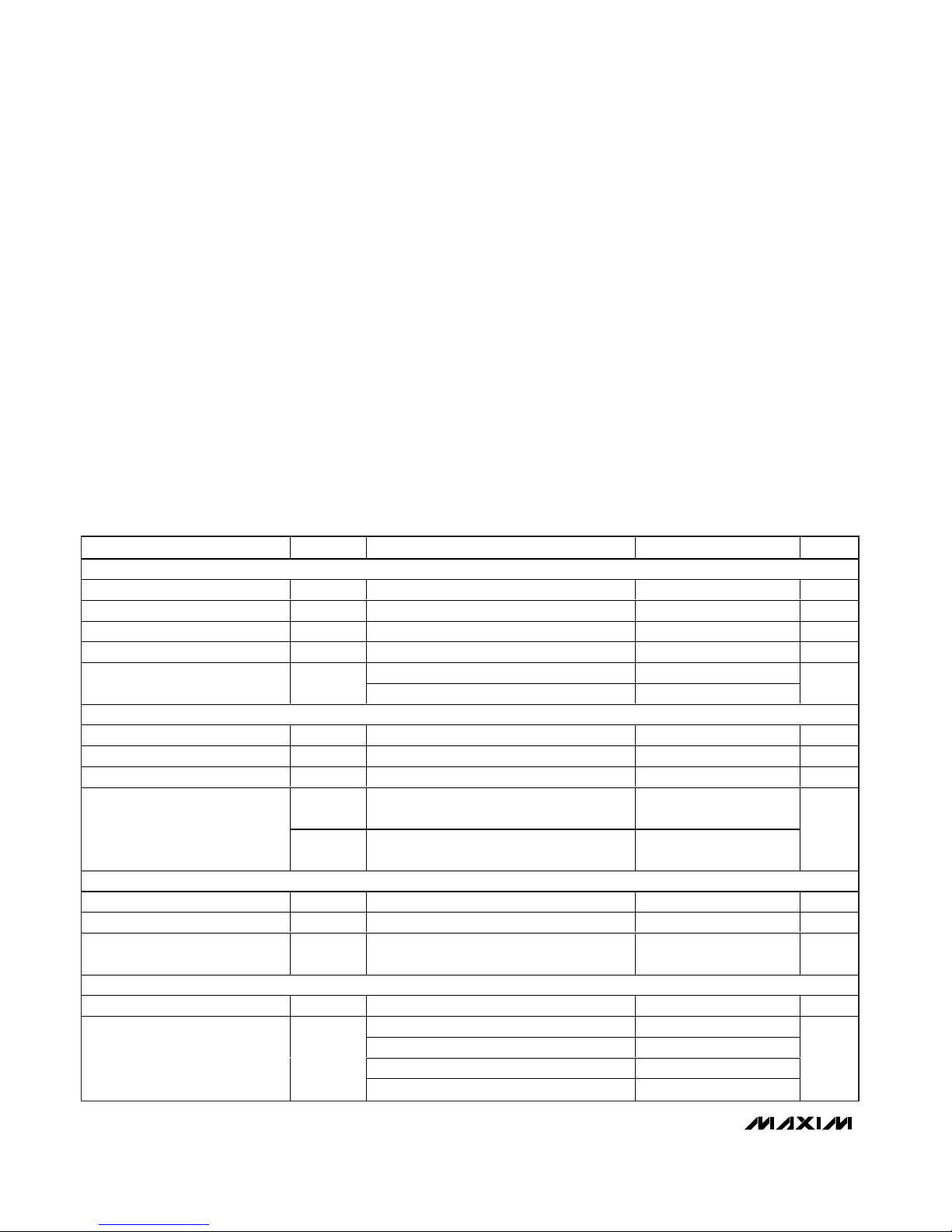
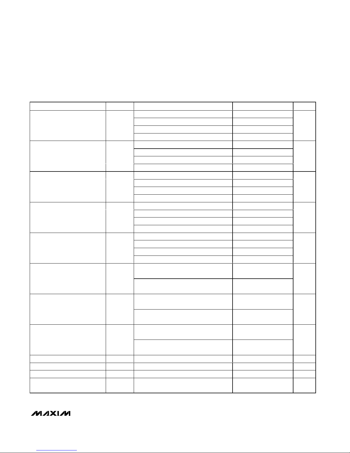
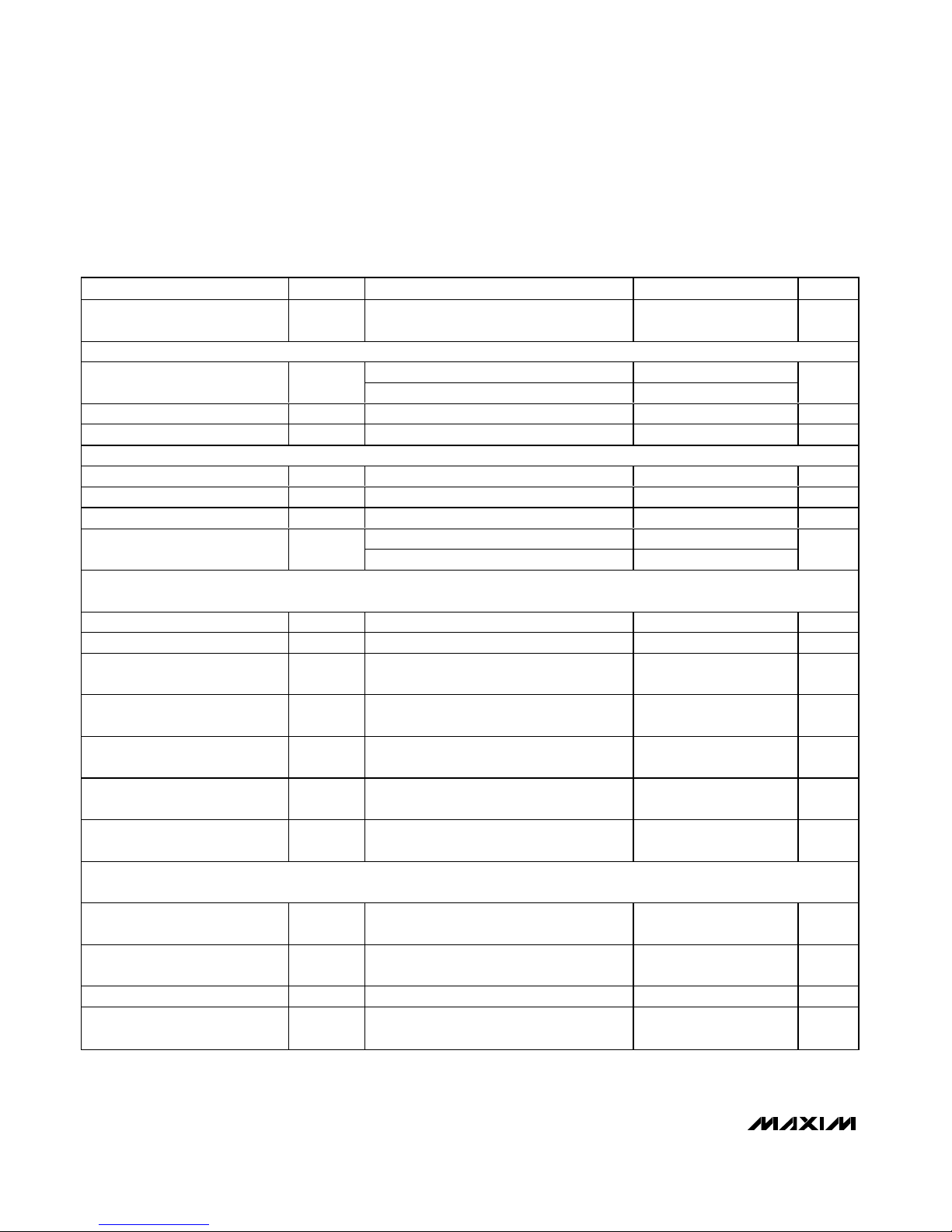
Maxim MAX12527 User manual

General Description
The MAX12527 is a dual 3.3V, 12-bit analog-to-digital
converter (ADC) featuring fully differential wideband
track-and-hold (T/H) inputs, driving internal quantizers.
The MAX12527 is optimized for low power, small size,
and high dynamic performance in intermediate frequen-
cy (IF) and baseband sampling applications. This dual
ADC operates from a single 3.3V supply, consuming
only 620mW while delivering a typical 69.8dB signal-to-
noise ratio (SNR) performance at a 175MHz input fre-
quency. The T/H input stages accept single-ended or
differential inputs up to 400MHz. In addition to low oper-
ating power, the MAX12527 features a 166µW power-
down mode to conserve power during idle periods.
A flexible reference structure allows the MAX12527 to
use the internal 2.048V bandgap reference or accept
an externally applied reference and allows the refer-
ence to be shared between the two ADCs. The refer-
ence structure allows the full-scale analog input range
to be adjusted from ±0.35V to ±1.15V. The MAX12527
provides a common-mode reference to simplify design
and reduce external component count in differential
analog input circuits.
The MAX12527 supports either a single-ended or differ-
ential input clock. User-selectable divide-by-two (DIV2)
and divide-by-four (DIV4) modes allow for design flexibil-
ity and help eliminate the negative effects of clock jitter.
Wide variations in the clock duty cycle are compensated
with the ADC’s internal duty-cycle equalizer (DCE).
The MAX12527 features two parallel, 12-bit-wide,
CMOS-compatible outputs. The digital output format is
pin-selectable to be either two’s complement or Gray
code. A separate power-supply input for the digital out-
puts accepts a 1.7V to 3.6V voltage for flexible interfac-
ing with various logic levels. The MAX12527 is available
in a 10mm x 10mm x 0.8mm, 68-pin thin QFN package
with exposed paddle (EP), and is specified for the
extended (-40°C to +85°C) temperature range.
For a 14-bit, pin-compatible version of this ADC, refer to
the MAX12557 data sheet.
Applications
IF and Baseband Communication Receivers
Cellular, LMDS, Point-to-Point Microwave,
MMDS, HFC, WLAN
I/Q Receivers
Ultrasound and Medical Imaging
Portable Instrumentation
Digital Set-Top Boxes
Low-Power Data Acquisition
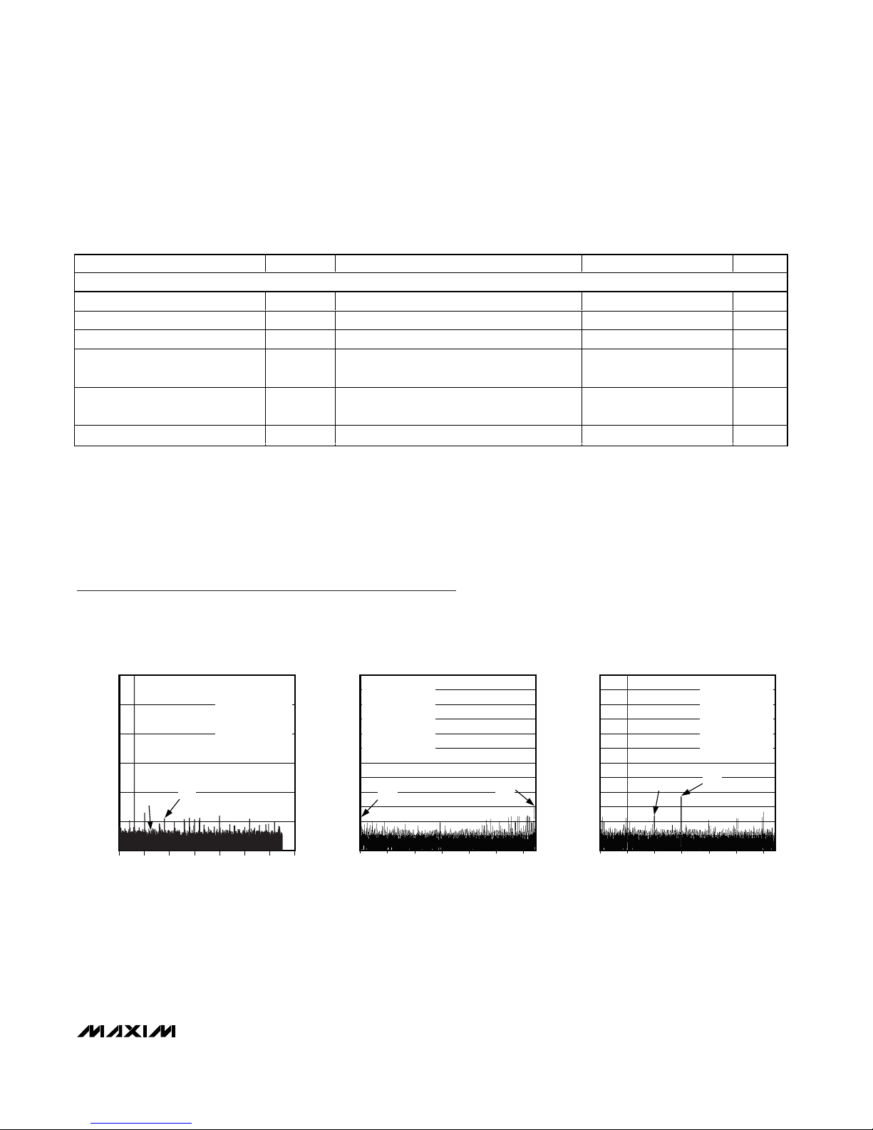
Features
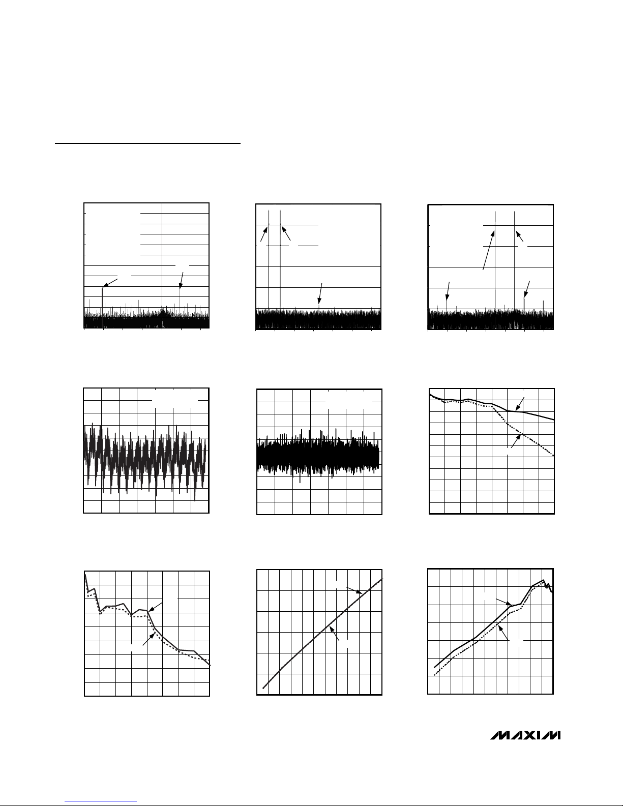
♦Direct IF Sampling Up to 400MHz
♦Excellent Dynamic Performance
70.4dB/69.8dB SNR at fIN = 70MHz/175MHz
84.4dBc/80.2dBc SFDR at fIN = 70MHz/175MHz
♦3.3V Low Power Operation
647mW (Differential Clock Mode)
620mW (Single-Ended Clock Mode)
♦Fully Differential or Single-Ended Analog Input
♦Adjustable Differential Analog Input Voltage
♦750MHz Input Bandwidth
♦Adjustable, Internal or External, Shared Reference
♦Differential or Single-Ended Clock
♦Accepts 25% to 75% Clock Duty Cycle
♦User-Selectable DIV2 and DIV4 Clock Modes
♦Power-Down Mode
♦CMOS Outputs in Two’s Complement or Gray
Code
♦Out-of-Range and Data-Valid Indicators
♦Small, 68-Pin Thin QFN Package
♦14-Bit Compatible Version Available (MAX12557)
♦Evaluation Kit Available (Order MAX12527 EV Kit)
MAX12527
Dual, 65Msps, 12-Bit, IF/Baseband ADC
________________________________________________________________ Maxim Integrated Products 1
Ordering Information
19-3543; Rev 0; 2/05
For pricing, delivery, and ordering information, please contact Maxim/Dallas Direct! at
1-888-629-4642, or visit Maxim’s website at www.maxim-ic.com.
EVALUATION KIT
AVAILABLE
PART
TEMP RANGE
PIN-PACKAGE
MAX12527ETK
-40°C to +85°C
68 Thin QFN-EP*
(10mm x 10mm x 0.8mm)
Pin Configuration appears at end of data sheet.
*EP = Exposed paddle.
PART
SAMPLING RATE
(Msps)
RESOLUTION
(Bits)
MAX12557 65 14
MAX12527 65 12
Selector Guide

MAX12527
Dual, 65Msps, 12-Bit, IF/Baseband ADC
2_______________________________________________________________________________________
ABSOLUTE MAXIMUM RATINGS
ELECTRICAL CHARACTERISTICS
(VDD = 3.3V, OVDD = 2.0V, GND = 0, REFIN = REFOUT (internal reference), CL≈10pF at digital outputs, VIN = -0.5dBFS (differen-
tial), DIFFCLK/SECLK = OVDD, PD = GND, SHREF = GND, DIV2 = GND, DIV4 = GND, G/T= GND, fCLK = 65MHz, TA= -40°C to
+85°C, unless otherwise noted. Typical values are at TA= +25°C.) (Note 1)
Stresses beyond those listed under “Absolute Maximum Ratings” may cause permanent damage to the device. These are stress ratings only, and functional
operation of the device at these or any other conditions beyond those indicated in the operational sections of the specifications is not implied. Exposure to
absolute maximum rating conditions for extended periods may affect device reliability.
VDD to GND................................................................-0.3V to +3.6V
OVDD to GND............-0.3V to the lower of (VDD + 0.3V) and +3.6V
INAP, INAN to GND ...-0.3V to the lower of (VDD + 0.3V) and +3.6V
INBP, INBN to GND ...-0.3V to the lower of (VDD + 0.3V) and +3.6V
CLKP, CLKN to
GND........................-0.3V to the lower of (VDD + 0.3V) and +3.6V
REFIN, REFOUT
to GND ..................-0.3V to the lower of (VDD + 0.3V) and +3.6V
REFAP, REFAN,
COMA to GND......-0.3V to the lower of (VDD + 0.3V) and +3.6V
REFBP, REFBN,
COMB to GND......-0.3V to the lower of (VDD + 0.3V) and +3.6V
DIFFCLK/SECLK, G/T, PD, SHREF, DIV2,
DIV4 to GND .........-0.3V to the lower of (VDD + 0.3V) and +3.6V
D0A–D11A, D0B–D11B, DAV,
DORA, DORB to GND..............................-0.3V to (OVDD + 0.3V)
Continuous Power Dissipation (TA= +70°C)
68-Pin Thin QFN 10mm x 10mm x 0.8mm
(derate 70mW/°C above +70°C) ....................................4000mW
Operating Temperature Range................................-40°C to +85°C
Junction Temperature...........................................................+150°C
Storage Temperature Range .................................-65°C to +150°C
Lead Temperature (soldering 10s).......................................+300°C
PARAMETER
SYMBOL
CONDITIONS
MIN TYP MAX
UNITS
DC ACCURACY
Resolution 12 Bits
Integral Nonlinearity INL fIN = 3MHz
±0.3 ±1.1
LSB
Differential Nonlinearity DNL fIN = 3MHz, no missing codes
±0.3 ±0.65
LSB
Offset Error
±0.1 ±0.7
%FSR
±0.5 ±5.7
Gain Error (Note 2)
±0.5 ±3.4
%FSR
ANALOG INPUT (INAP, INAN, INBP, INBN)
Differential Input Voltage Range VDIFF Differential or single-ended inputs
±1.024
V
Common-Mode Input Voltage
VDD / 2
V
Analog Input Resistance RIN Each input (Figure 3) 3.4 kΩ
CPAR Fixed capacitance to ground,
each input (Figure 3) 2
Analog Input Capacitance
CSAMPLE
Switched capacitance,
each input (Figure 3) 4.5 pF
CONVERSION RATE
Maximum Clock Frequency fCLK 65 MHz
Minimum Clock Frequency 5MHz
Data Latency Figure 5 8
Clock
Cycles
DYNAMIC CHARACTERISTICS (differential inputs)
Small-Signal Noise Floor SSNF Input at -35dBFS (Note 2)
67.0 71.1
dBFS
fIN = 3MHz at -0.5dBFS
68.2 70.8
fIN = 32.5MHz at -0.5dBFS
70.6
fIN = 70MHz at -0.5dBFS
70.4
Signal-to-Noise Ratio SNR
fIN = 175MHz at -0.5dBFS
67.2 69.8
dB

MAX12527
Dual, 65Msps, 12-Bit, IF/Baseband ADC
_______________________________________________________________________________________ 3
ELECTRICAL CHARACTERISTICS (continued)
(VDD = 3.3V, OVDD = 2.0V, GND = 0, REFIN = REFOUT (internal reference), CL≈10pF at digital outputs, VIN = -0.5dBFS (differen-
tial), DIFFCLK/SECLK = OVDD, PD = GND, SHREF = GND, DIV2 = GND, DIV4 = GND, G/T= GND, fCLK = 65MHz, TA= -40°C to
+85°C, unless otherwise noted. Typical values are at TA= +25°C.) (Note 1)
PARAMETER
SYMBOL
CONDITIONS
MIN TYP MAX UNITS
fIN = 3MHz at -0.5dBFS
68.1 70.7
fIN = 32.5MHz at -0.5dBFS
70.4
fIN = 70MHz at -0.5dBFS
70.2
Signal-to-Noise Plus Distortion SINAD
fIN = 175MHz at -0.5dBFS
65.9 69.3
dB
fIN = 3MHz at -0.5dBFS (Note 2)
81.9
91
fIN = 32.5MHz at -0.5dBFS
86.3
fIN = 70MHz at -0.5dBFS
84.4
Spurious-Free Dynamic Range SFDR
fIN = 175MHz at -0.5dBFS
71.1 80.2
dBc
fIN = 3MHz at -0.5dBFS (Note 2)
-92.6 -82.9
fIN = 32.5MHz at -0.5dBFS
-84.3
fIN = 70MHz at -0.5dBFS
-83.7
Total Harmonic Distortion THD
fIN = 175MHz at -0.5dBFS
-78.9 -69.8
dBc
fIN = 3MHz at -0.5dBFS -98
fIN = 32.5MHz at -0.5dBFS
-91.7
fIN = 70MHz at -0.5dBFS
-94.5
Second Harmonic HD2
fIN = 175MHz at -0.5dBFS
-80.2
dBc
fIN = 3MHz at -0.5dBFS -97
fIN = 32.5MHz at -0.5dBFS
-86.3
fIN = 70MHz at -0.5dBFS
-84.4
Third Harmonic HD3
fIN = 175MHz at -0.5dBFS
-85.6
dBc
fIN1 = 68.5MHz at -7dBFS
fIN2 = 71.5MHz at -7dBFS -89
Two-Tone Intermodulation
Distortion (Note 3) TTIMD fIN1 = 172.5MHz at -7dBFS
fIN2 = 177.5MHz at -7dBFS
-82.2
dBc
fIN1 = 68.5MHz at -7dBFS
fIN2 = 71.5MHz at -7dBFS
-92.2
3rd-Order Intermodulation
Distortion IM3 fIN1 = 172.5MHz at -7dBFS
fIN2 = 177.5MHz at -7dBFS
-88.9
dBc
fIN1 = 68.5MHz at -7dBFS
fIN2 = 71.5MHz at -7dBFS
90.6
Two-Tone Spurious-Free
Dynamic Range
SFDRTT
fIN1 = 172.5MHz at -7dBFS
fIN2 = 177.5MHz at -7dBFS
82.9
dBc
Full-Power Bandwidth FPBW Input at -0.2dBFS, -3dB rolloff
750
MHz
Aperture Delay tAD Figure 5 1.2 ns
Aperture Jitter tAJ
<0.15 psRMS
Output Noise nOUT INAP = INAN = COMA
INBP = INBN = COMB 0.3
LSBRMS

MAX12527
Dual, 65Msps, 12-Bit, IF/Baseband ADC
4_______________________________________________________________________________________
ELECTRICAL CHARACTERISTICS (continued)
(VDD = 3.3V, OVDD = 2.0V, GND = 0, REFIN = REFOUT (internal reference), CL≈10pF at digital outputs, VIN = -0.5dBFS (differen-
tial), DIFFCLK/SECLK = OVDD, PD = GND, SHREF = GND, DIV2 = GND, DIV4 = GND, G/T= GND, fCLK = 65MHz, TA= -40°C to
+85°C, unless otherwise noted. Typical values are at TA= +25°C.) (Note 1)
PARAMETER
SYMBOL
CONDITIONS
MIN TYP MAX
UNITS
Overdrive Recovery Time ±10% beyond full-scale 1 Clock
cycle
INTERCHANNEL CHARACTERISTICS
fINA or fINB = 70MHz at -0.5dBFS 90
Crosstalk Rejection fINA or fINB = 175MHz at -0.5dBFS 85 dB
Gain Matching
±0.01 ±0.1
dB
Offset Matching
±0.01
%FSR
INTERNAL REFERENCE (REFOUT)
REFOUT Output Voltage
VREFOUT 2.000 2.048 2.080
V
REFOUT Load Regulation -1mA < IREFOUT < +1mA 35
mV/mA
REFOUT Temperature Coefficient
TCREF
±50
ppm/°C
Short to VDD—sinking
0.24
REFOUT Short-Circuit Current Short to GND—sourcing 2.1 mA
BUFFERED REFERENCE MODE (REFIN is driven by REFOUT or an external 2.048V single-ended reference source;
VREFAP/VREFAN/VCOMA and VREFBP/VREFBN/VCOMB are generated internally)
REFIN Input Voltage VREFIN
2.048
V
REFIN Input Resistance RREFIN
>50
MΩ
COM_ Output Voltage VCOMA
VCOMB VDD / 2
1.60 1.65 1.70
V
REF_P Output Voltage VREFAP
VREFBP
VDD / 2 + (VREFIN x 3/8)
2.418
V
REF_N Output Voltage VREFAN
VREFBN
VDD / 2 - (VREFIN x 3/8)
0.882
V
Differential Reference Voltage VREFA
VREFB VREFA = VREFAP - VREFAN
VREFB = VREFBP - VREFBN
1.440 1.536 1.590
V
Differential Reference
Temperature Coefficient TCREF
±25
ppm/°C
UNBUFFERED EXTERNAL REFERENCE (REFIN = GND, VREFAP/VREFAN/VCOMA and VREFBP/VREFBN/VCOMB are applied
externally, VCOMA = VCOMB = VDD / 2)
REF_P Input Voltage VREFAP
VREFBP
VREF_P - VCOM
+0.768
V
REF_N Input Voltage VREFAN
VREFBN
VREF_N - VCOM
-0.768
V
COM_ Input Voltage VCOM VDD / 2
1.65
V
Differential Reference Voltage VREFA
VREFB VREF_ = VREF_P - VREF_N = VREFIN x 3/4
1.536
V

MAX12527
Dual, 65Msps, 12-Bit, IF/Baseband ADC
_______________________________________________________________________________________ 5
ELECTRICAL CHARACTERISTICS (continued)
(VDD = 3.3V, OVDD = 2.0V, GND = 0, REFIN = REFOUT (internal reference), CL≈10pF at digital outputs, VIN = -0.5dBFS (differen-
tial), DIFFCLK/SECLK = OVDD, PD = GND, SHREF = GND, DIV2 = GND, DIV4 = GND, G/T= GND, fCLK = 65MHz, TA= -40°C to
+85°C, unless otherwise noted. Typical values are at TA= +25°C.) (Note 1)
PARAMETER
SYMBOL
CONDITIONS
MIN TYP MAX
UNITS
REF_P Sink Current IREFAP
IREFBP VREF_P = 2.418V 1.2 mA
REF_N Source Current IREFAN
IREFBN VREF_N = 0.882V
0.85
mA
COM_ Sink Current ICOMA
ICOMB VCOM_ = 1.65V
0.85
mA
REF_P, REF_N Capacitance CREF_P,
CREF_N
13 pF
COM_ Capacitance CCOM_ 6pF
CLOCK INPUTS (CLKP, CLKN)
Single-Ended Input High
Threshold VIH DIFFCLK/SECLK = GND, CLKN = GND 0.8 x
VDD
V
Single-Ended Input Low
Threshold VIL DIFFCLK/SECLK = GND, CLKN = GND 0.2 x
VDD
V
Minimum Differential Clock Input
Voltage Swing DIFFCLK/SECLK = OVDD 0.2 VP-P
Differential Input Common-Mode
Voltage DIFFCLK/SECLK = OVDD
VDD / 2
V
CLK_ Input Resistance RCLK Each input (Figure 4) 5 kΩ
CLK_ Input Capacitance CCLK Each input 2 pF
DIGITAL INPUTS (DIFFCLK/SECLK, G/T, PD, DIV2, DIV4)
Input High Threshold VIH 0.8 x
OVDD
V
Input Low Threshold VIL 0.2 x
OVDD
V
OVDD applied to input ±5
Input Leakage Current Input connected to ground ±5 µA
Digital Input Capacitance CDIN 5pF
DIGITAL OUTPUTS (D0A–D11A, D0B–D11B, DORA, DORB, DAV)
D0A–D11A, D0B–D11B, DORA, DORB:
ISINK = 200µA 0.2
Output-Voltage Low VOL DAV: ISINK = 600µA 0.2 V
D0A–D11A, D0B–D11B, DORA, DORB:
ISOURCE = 200µA OVDD -
0.2
Output-Voltage High VOH DAV: ISOURCE = 600µA OVDD -
0.2
V
OVDD applied to input ±5
Tri-State Leakage Current
(Note 4) ILEAK Input connected to ground ±5 µA

MAX12527
Dual, 65Msps, 12-Bit, IF/Baseband ADC
6_______________________________________________________________________________________
ELECTRICAL CHARACTERISTICS (continued)
(VDD = 3.3V, OVDD = 2.0V, GND = 0, REFIN = REFOUT (internal reference), CL≈10pF at digital outputs, VIN = -0.5dBFS (differen-
tial), DIFFCLK/SECLK = OVDD, PD = GND, SHREF = GND, DIV2 = GND, DIV4 = GND, G/T= GND, fCLK = 65MHz, TA= -40°C to
+85°C, unless otherwise noted. Typical values are at TA= +25°C.) (Note 1)
PARAMETER
SYMBOL
CONDITIONS
MIN TYP MAX
UNITS
D0A–D11A, DORA,
D0B–D11B and DORB Tri-State
Output Capacitance (Note 4) COUT 3pF
DAV Tri-State Output
Capacitance (Note 4) CDAV 6pF
POWER REQUIREMENTS
Analog Supply Voltage VDD
3.15 3.30 3.60
V
Digital Output Supply Voltage OVDD
1.70
2.0
VDD
V
Normal operating mode
fIN = 175MHz at -0.5dBFS,
single-ended clock
(DIFFCLK/SECLK = GND)
188
Normal operating mode
fIN = 175MHz at -0.5dBFS
differential clock
(DIFFCLK/SECLK = OVDD)
196 215
Analog Supply Current IVDD
Power-down mode (PD = OVDD)
clock idle
0.05
mA
Normal operating mode
fIN = 175MHz at -0.5dBFS
single-ended clock
(DIFFCLK/SECLK = GND)
620
Normal operating mode
fIN = 175MHz at -0.5dBFS
differential clock
(DIFFCLK/SECLK = OVDD)
647 710
Analog Power Dissipation PVDD
Power-down mode (PD = OVDD)
clock idle
0.165
mW
Normal operating mode
fIN = 175MHz at -0.5dBFS
19.7
Digital Output Supply Current IOVDD Power-down mode (PD = OVDD)
clock idle
0.001
mA

MAX12527
Dual, 65Msps, 12-Bit, IF/Baseband ADC
_______________________________________________________________________________________ 7
ELECTRICAL CHARACTERISTICS (continued)
(VDD = 3.3V, OVDD = 2.0V, GND = 0, REFIN = REFOUT (internal reference), CL≈10pF at digital outputs, VIN = -0.5dBFS (differen-
tial), DIFFCLK/SECLK = OVDD, PD = GND, SHREF = GND, DIV2 = GND, DIV4 = GND, G/T= GND, fCLK = 65MHz, TA= -40°C to
+85°C, unless otherwise noted. Typical values are at TA= +25°C.) (Note 1)
PARAMETER
SYMBOL
CONDITIONS
MIN
TYP
MAX
UNITS
TIMING CHARACTERISTICS (Figure 5)
Clock Pulse-Width High tCH 7.7 ns
Clock Pulse-Width Low tCL 7.7 ns
Data-Valid Delay tDAV 5.4 ns
Data Setup Time Before Rising
Edge of DAV tSETUP (Note 5) 7.0 ns
Data Hold Time After Rising Edge
of DAV tHOLD (Note 5) 7.0 ns
Wake-Up Time from Power-Down
tWAKE VREFIN = 2.048V 10 ms
Note 1: Specifications ≥+25°C guaranteed by production test, <+25°C guaranteed by design and characterization.
Note 2: Specifications guaranteed by production test for ≥+25°C.
Note 3: Two-tone intermodulation distortion measured with respect to a single-carrier amplitude, and not the peak-to-average input
power of both input tones.
Note 4: During power-down, D0A–D11A, D0B–D11B, DORA, DORB, and DAV are high impedance.
Note 5: Guaranteed by design and characterization.
Typical Operating Characteristics
(VDD = 3.3V, OVDD = 2.0V, GND = 0, REFIN = REFOUT (internal reference mode), CL≈5pF at digital outputs, VIN = -0.5dBFS,
DIFFCLK/SECLK = OVDD, PD = GND, G/T= GND, fCLK = 65MHz (50% duty cycle), TA= +25°C, unless otherwise noted.)
FFT PLOT (16,384-POINT DATA RECORD)
MAX12527 toc01
ANALOG INPUT FREQUENCY (MHz)
AMPLITUDE (dBFS)
30252015105
-100
-80
-60
-40
-20
0
-120
035
fCLK = 65MHz
fIN = 3.00125MHz
AIN = -0.53dBFS
SNR = 71dB
SINAD = 70.9dB
THD = -94dBc
SFDR = 93.6dBc
HD2 HD3
FFT PLOT (32,768-POINT DATA RECORD)
MAX12527 toc02
ANALOG INPUT FREQUENCY (MHz)
AMPLITUDE (dBFS)
302515 20105
-110
-100
-90
-80
-70
-60
-50
-40
-30
-20
-10
0
-120
0
fCLK = 65.00352MHz
fIN = 32.40059MHz
AIN = -0.506dBFS
SNR = 70.5dB
SINAD = 70.2dB
THD = -86.9dBc
SFDR = 88.7dBc
HD2 HD3
FFT PLOT (32,768-POINT DATA RECORD)
MAX12527 toc03
ANALOG INPUT FREQUENCY (MHz)
AMPLITUDE (dBFS)
302515 20105
-110
-100
-90
-80
-70
-60
-50
-40
-30
-20
-10
0
-120
0
fCLK = 65.00352MHz
fIN = 70.00852MHz
AIN = -0.506dBFS
SNR = 70.1dB
SINAD = 69.8dB
THD = -82.1dBc
SFDR = 82.4dBc
HD2 HD3

MAX12527
Dual, 65Msps, 12-Bit, IF/Baseband ADC
8_______________________________________________________________________________________
INTEGRAL NONLINEARITY
vs. DIGITAL OUTPUT CODE
MAX12527 toc07
DIGITAL OUTPUT CODE
INL (LSB)
360030001800 24001200600
-0.4
-0.3
-0.2
-0.1
0
0.1
0.2
0.3
0.4
0.5
-0.5
0 4200
fCLK = 65MHz
fIN = 3.00119MHz
DIFFERENTIAL NONLINEARITY
vs. DIGITAL OUTPUT CODE
MAX12527 toc08
DIGITAL OUTPUT CODE
DNL (LSB)
360030001800 24001200600
-0.4
-0.3
-0.2
-0.1
0
0.1
0.2
0.3
0.4
0.5
-0.5
0 4200
fCLK = 65MHz
fIN = 3.00119MHz
SNR, SINAD vs. ANALOG INPUT FREQUENCY
(fCLK = 65.00352MHz, AIN = -0.5dBFS)
MAX12527 toc09
fIN (MHz)
SNR, SINAD (dB)
350300200 250100 15050
52
54
56
58
60
62
64
66
68
70
72
50
0 400
SINAD
SNR
-THD, SFDR vs. ANALOG INPUT FREQUENCY
(fCLK = 65.00352MHz, AIN = -0.5dBFS)
MAX12527 toc10
fIN (MHz)
-THD, SFDR (dBc)
350300200 250100 15050
55
60
65
70
75
80
85
90
95
50
0 400
SFDR
-THD
SNR, SINAD vs. ANALOG INPUT AMPLITUDE
(fCLK = 65.00352MHz, fIN = 70MHz)
MAX12527 toc11
AIN (dBFS)
SNR, SINAD (dB)
-5-10-15-20-25-30-35-40-45-50
25
35
45
55
65
75
15
-55 0
SNR
SINAD
-THD, SFDR vs. ANALOG INPUT AMPLITUDE
(fCLK = 65.00352MHz, fIN = 70MHz)
MAX12527 toc12
AIN (dBFS)
-THD, SFDR (dBc)
-5-10-15-20-25-30-35-40-45-50
35
45
55
65
75
85
95
25
-55 0
SFDR
-THD
FFT PLOT (32,768-POINT DATA RECORD)
MAX12527 toc04
ANALOG INPUT FREQUENCY (MHz)
AMPLITUDE (dBFS)
302515 20105
-110
-100
-90
-80
-70
-60
-50
-40
-30
-20
-10
0
-120
0
fCLK = 65.00352MHz
fIN = 174.90525MHz
AIN = -0.448dBFS
SNR = 69.4dB
SINAD = 68.9dB
THD = -78.6dBc
SFDR = 81.1dBc
HD2
HD3
TWO-TONE IMD PLOT
(16,384-POINT DATA RECORD)
MAX12527 toc05
ANALOG INPUT FREQUENCY (MHz)
AMPLITUDE (dBFS)
30252015105
-100
-80
-60
-40
-20
0
-120
0
fCLK = 65.00352MHz
fIN1 = 68.49889MHz
fIN2 = 71.49832MHz
AIN1 = -6.96dBFS
AIN2 = -7.02dBFS
IM3 = -92.25dBc
IMD = -89.08dBc
fIN1 fIN2
2fIN2 + fIN1
TWO-TONE IMD PLOT
(16,384-POINT DATA RECORD)
MAX12527 toc06
ANALOG INPUT FREQUENCY (MHz)
AMPLITUDE (dBFS)
30252015105
-100
-80
-60
-40
-20
0
-120
0
fCLK = 65.00352MHz
fIN1 = 172.50293MHz
AIN1 = -6.99dBFS
fIN2 = 177.40198MHz
AIN2 = -7.01dBFS
IM3 = -88.88dBc
IMD = -82.24dBc
fIN1
fIN2 fIN1 + fIN2
fIN2 - fIN1
Typical Operating Characteristics (continued)
(VDD = 3.3V, OVDD = 2.0V, GND = 0, REFIN = REFOUT (internal reference mode), CL≈5pF at digital outputs, VIN = -0.5dBFS,
DIFFCLK/SECLK = OVDD, PD = GND, G/T= GND, fCLK = 65MHz (50% duty cycle), TA= +25°C, unless otherwise noted.)

MAX12527
Dual, 65Msps, 12-Bit, IF/Baseband ADC
_______________________________________________________________________________________ 9
SNR, SINAD vs. ANALOG INPUT AMPLITUDE
(fCLK = 65.00352MHz, fIN = 175MHz)
MAX12527 toc13
AIN (dBFS)
SNR, SINAD (dB)
-5-10-15-20-25-30-35-40-45-50
25
35
45
55
65
75
15
-55 0
SNR
SINAD
-THD, SFDR vs. ANALOG INPUT AMPLITUDE
(fCLK = 65.00352MHz, fIN = 175MHz)
MAX12527 toc14
AIN (dBFS)
-THD, SFDR (dBc)
-5-10-15-20-25-30-35-40-45-50
35
45
55
65
75
85
95
25
-55 0
SFDR
-THD
SNR, SINAD vs. CLOCK SPEED
(fIN = 70MHz, AIN = -0.5dBFS)
MAX12527 toc15
fCLK (MHz)
SNR, SINAD (dB)
6055504540353025
62
64
66
68
70
72
60
20 65
SNR
SINAD
-THD, SFDR vs. CLOCK SPEED
(fIN = 70MHz, AIN = -0.5dBFS)
MAX12527 toc16
fCLK (MHz)
-THD, SFDR (dBc)
6055504540353025
65
70
75
80
85
90
60
20 65
SFDR
-THD
SNR, SINAD vs. CLOCK SPEED
(fIN = 175MHz, AIN = -0.5dBFS)
MAX12527 toc17
fCLK (MHz)
SNR, SINAD (dB)
6055504540353025
62
64
66
68
70
72
60
20 65
SNR
SINAD
-THD, SFDR vs. CLOCK SPEED
(fIN = 175MHz, AIN = -0.5dBFS)
MAX12527 toc18
fCLK (MHz)
-THD, SFDR (dBc)
6055504540353025
65
70
75
80
85
90
60
20 65
SFDR
-THD
SNR, SINAD vs. ANALOG SUPPLY VOLTAGE
(fCLK = 65.00352MHz, fIN = 70MHz)
MAX12527 toc19
VDD (V)
SNR, SINAD (dB)
3.53.43.33.23.1
62
64
66
68
70
72
60
3.0 3.6
SINAD
SNR
-THD, SFDR vs. ANALOG SUPPLY VOLTAGE
(fCLK = 65.00352MHz, fIN = 70MHz)
MAX12527 toc20
VDD (V)
-THD, SFDR (dBc)
3.53.43.33.23.1
65
70
75
80
85
90
60
3.0 3.6
-THD
SFDR
SNR, SINAD vs. ANALOG SUPPLY VOLTAGE
(fCLK = 65.00352MHz, fIN = 175MHz)
MAX12527 toc21
VDD (V)
SNR, SINAD (dB)
3.53.43.33.23.1
62
64
66
68
70
72
60
3.0 3.6
SINAD
SNR
Typical Operating Characteristics (continued)
(VDD = 3.3V, OVDD = 2.0V, GND = 0, REFIN = REFOUT (internal reference mode), CL≈5pF at digital outputs, VIN = -0.5dBFS,
DIFFCLK/SECLK = OVDD, PD = GND, G/T= GND, fCLK = 65MHz (50% duty cycle), TA= +25°C, unless otherwise noted.)

MAX12527
Dual, 65Msps, 12-Bit, IF/Baseband ADC
10 ______________________________________________________________________________________
-THD, SFDR vs. ANALOG SUPPLY VOLTAGE
(fCLK = 65.00352MHz, fIN = 175MHz)
MAX12527 toc22
VDD (V)
-THD, SFDR (dBc)
3.53.43.33.23.1
65
70
75
80
85
90
60
3.0 3.6
-THD
SFDR
SNR, SINAD vs. DIGITAL SUPPLY VOLTAGE
(fCLK = 65.00352MHz, fIN = 70MHz)
MAX12527 toc23
OVDD (V)
SNR, SINAD (dB)
3.33.02.72.42.11.8
62
64
66
68
70
72
60
1.5 3.6
SNR
SINAD
-THD, SFDR vs. DIGITAL SUPPLY VOLTAGE
(fCLK = 65.00352MHz, fIN = 70MHz)
MAX12527 toc24
OVDD (V)
-THD, SFDR (dBc)
3.33.02.72.42.11.8
65
70
75
80
85
90
60
1.5 3.6
-THD
SFDR
SNR, SINAD vs. DIGITAL SUPPLY VOLTAGE
(fCLK = 65.00352MHz, fIN = 175MHz)
MAX12527 toc25
OVDD (V)
SNR, SINAD (dB)
3.33.02.72.42.11.8
62
64
66
68
70
72
60
1.5 3.6
SNR
SINAD
-THD, SFDR vs. DIGITAL SUPPLY VOLTAGE
(fCLK = 65.00352MHz, fIN = 175MHz)
MAX12527 toc26
OVDD (V)
-THD, SFDR (dBc)
3.33.02.72.42.11.8
65
70
75
80
85
90
60
1.5 3.6
-THD
SFDR
PDISS, IVDD (ANALOG) vs. ANALOG SUPPLY VOLTAGE
(fCLK = 65.00352MHz, fIN = 175MHz)
MAX12527 toc27
VDD (V)
PDISS, IVDD (mW, mA)
3.53.43.33.23.1
100
200
300
400
500
600
700
800
900
0
3.0 3.6
PDISS (ANALOG)
IVDD
PDISS, IOVDD (DIGITAL) vs. DIGITAL SUPPLY VOLTAGE
(fCLK = 65.00352MHz, fIN = 175MHz)
MAX12527 toc28
OVDD (V)
PDISS, IOVDD (mW, mA)
3.33.01.8 2.1 2.4 2.7
10
20
30
40
50
60
70
80
0
1.5 3.6
PDISS (DIGITAL)
CL ≈5pF
IOVDD
SNR, SINAD vs. CLOCK DUTY CYCLE
(fIN = 70MHz, AIN = -0.5dBFS)
MAX12527 toc29
CLOCK DUTY CYCLE (%)
SNR, SINAD (dB)
65554535
62
64
66
68
70
72
60
25 75
SNR
SINAD
SINGLE-ENDED CLOCK INPUT DRIVE
-THD, SFDR vs. CLOCK DUTY CYCLE
(fIN = 70MHz, AIN = -0.5dBFS)
MAX12527 toc30
CLOCK DUTY CYCLE (%)
-THD, SFDR (dBc)
65554535
65
70
75
80
85
90
60
25 75
-THD
SFDR
SINGLE-ENDED CLOCK INPUT DRIVE
Typical Operating Characteristics (continued)
(VDD = 3.3V, OVDD = 2.0V, GND = 0, REFIN = REFOUT (internal reference mode), CL≈5pF at digital outputs, VIN = -0.5dBFS,
DIFFCLK/SECLK = OVDD, PD = GND, G/T= GND, fCLK = 65MHz (50% duty cycle), TA= +25°C, unless otherwise noted.)

MAX12527
Dual, 65Msps, 12-Bit, IF/Baseband ADC
______________________________________________________________________________________ 11
SNR, SINAD vs. TEMPERATURE
(fIN = 175MHz, AIN = -0.5dBFS)
MAX12527 toc31
TEMPERATURE (°C)
SNR, SINAD (dB)
603510-15
62
64
66
68
70
72
60
-40 85
SNR
SINAD
-THD, SFDR vs. TEMPERATURE
(fIN = 175MHz, AIN = -0.5dBFS)
MAX12527 toc32
TEMPERATURE (°C)
-THD, SFDR (dBc)
603510-15
65
70
75
80
85
90
60
-40 85
-THD
SFDR
GAIN ERROR vs. TEMPERATURE
MAX12527 toc33
TEMPERATURE (°C)
GAIN ERROR (%FSR)
603510-15
-2
-1
0
1
2
3
-3
-40 85
OFFSET ERROR vs. TEMPERATURE
MAX12527 toc34
TEMPERATURE (°C)
OFFSET ERROR (% FSR)
6035-15 10
-0.2
-0.1
0
0.1
0.2
0.3
-0.3
-40 85
Typical Operating Characteristics (continued)
(VDD = 3.3V, OVDD = 2.0V, GND = 0, REFIN = REFOUT (internal reference mode), CL≈5pF at digital outputs, VIN = -0.5dBFS,
DIFFCLK/SECLK = OVDD, PD = GND, G/T= GND, fCLK = 65MHz (50% duty cycle), TA= +25°C, unless otherwise noted.)

MAX12527
Dual, 65Msps, 12-Bit, IF/Baseband ADC
12 ______________________________________________________________________________________
PIN NAME FUNCTION
1, 4, 5, 9,
13, 14, 17
GND Converter Ground. Connect all ground pins and the exposed paddle (EP) together.
2INAP Channel A Positive Analog Input
3INAN Channel A Negative Analog Input
6COMA Channel A Common-Mode Voltage I/O. Bypass COMA to GND with a 0.1µF capacitor.
7REFAP
Channel A Positive Reference I/O. Channel A conversion range is ±2/3 x (VREFAP - VREFAN). Bypass
REFAP with a 0.1µF capacitor to GND. Connect a 10µF and a 1µF bypass capacitor between REFAP
and REFAN. Place the 1µF REFAP-to-REFAN capacitor as close to the device as possible on the
same side of the PC board.
8REFAN
Channel A Negative Reference I/O. Channel A conversion range is ±2/3 x (VREFAP - VREFAN). Bypass
REFAN with a 0.1µF capacitor to GND. Connect a 10µF and a 1µF bypass capacitor between REFAP
and REFAN. Place the 1µF REFAP-to-REFAN capacitor as close to the device as possible on the
same side of the PC board.
10 REFBN
Channel B Negative Reference I/O. Channel B conversion range is ±2/3 x (VREFBP - VREFBN). Bypass
REFBN with a 0.1µF capacitor to GND. Connect a 10µF and a 1µF bypass capacitor between REFBP
and REFBN. Place the 1µF REFBP-to-REFBN capacitor as close to the device as possible on the
same side of the PC board.
11 REFBP
Channel B Positive Reference I/O. Channel B conversion range is ±2/3 x (VREFBP - VREFBN). Bypass
REFBP with a 0.1µF capacitor to GND. Connect a 10µF and a 1µF bypass capacitor between REFBP
and REFBN. Place the 1µF REFBP-to-REFBN capacitor as close to the device as possible on the
same side of the PC board.
12 COMB Channel A Common-Mode Voltage I/O. Bypass COMB to GND with a 0.1µF capacitor.
15 INBN Channel B Negative Analog Input
16 INBP Channel B Positive Analog Input
18
DIFFCLK/
SECLK
Differential/Single-Ended Input Clock Drive. This input selects between single-ended or differential clock
input drives.
DIFFCLK/SECLK = GND: Selects single-ended clock input drive.
DIFFCLK/SECLK = OVDD: Selects differential clock input drive.
19 CLKN Negative Clock Input. In differential clock input mode (DIFFCLK/SECLK = OVDD), connect a differential
clock signal between CLKP and CLKN. In single-ended clock mode (DIFFCLK/SECLK = GND), apply the
clock signal to CLKP and connect CLKN to GND.
20 CLKP Positive Clock Input. In differential clock input mode (DIFFCLK/SECLK = OVDD), connect a differential
clock signal between CLKP and CLKN. In single-ended clock mode (DIFFCLK/SECLK = GND), apply
the single-ended clock signal to CLKP and connect CLKN to GND.
21 DIV2 Divide-by-Two Clock-Divider Digital Control Input. See Table 2 for details.
22 DIV4 Divide-by-Four Clock-Divider Digital Control Input. See Table 2 for details.
23–26, 61,
62, 63 VDD Analog Power Input. Connect VDD to a 3.15V to 3.60V power supply. Bypass VDD to GND with a parallel
capacitor combination of ≥10µF and 0.1µF. Connect all VDD pins to the same potential.
27, 43, 60
OVDD Output-Driver Power Input. Connect OVDD to a 1.7V to VDD power supply. Bypass OVDD to GND with a
parallel capacitor combination of ≥10µF and 0.1µF.
28, 29, 45,
46 N.C. No Connection
Pin Description

MAX12527
Dual, 65Msps, 12-Bit, IF/Baseband ADC
______________________________________________________________________________________ 13
PIN NAME FUNCTION
30 D0B Channel B CMOS Digital Output, Bit 0 (LSB)
31 D1B Channel B CMOS Digital Output, Bit 1
32 D2B Channel B CMOS Digital Output, Bit 2
33 D3B Channel B CMOS Digital Output, Bit 3
34 D4B Channel B CMOS Digital Output, Bit 4
35 D5B Channel B CMOS Digital Output, Bit 5
36 D6B Channel B CMOS Digital Output, Bit 6
37 D7B Channel B CMOS Digital Output, Bit 7
38 D8B Channel B CMOS Digital Output, Bit 8
39 D9B Channel B CMOS Digital Output, Bit 9
40 D10B Channel B CMOS Digital Output, Bit 10
41 D11B Channel B CMOS Digital Output, Bit 11 (MSB)
42 DORB
Channel B Data Out-of-Range Indicator. The DORB digital output indicates when the channel B analog
input voltage is out of range.
DORB = 1: Digital outputs exceed full-scale range.
DORB = 0: Digital outputs are within full-scale range.
44 DAV Data-Valid Digital Output. The rising edge of DAV indicates that data is present on the digital outputs.
The MAX12527 evaluation kit (MAX12557 EV kit) utilizes DAV to latch data into any external back-end
digital logic.
47 D0A Channel A CMOS Digital Output, Bit 0 (LSB)
48 D1A Channel A CMOS Digital Output, Bit 1
49 D2A Channel A CMOS Digital Output, Bit 2
50 D3A Channel A CMOS Digital Output, Bit 3
51 D4A Channel A CMOS Digital Output, Bit 4
52 D5A Channel A CMOS Digital Output, Bit 5
53 D6A Channel A CMOS Digital Output, Bit 6
54 D7A Channel A CMOS Digital Output, Bit 7
55 D8A Channel A CMOS Digital Output, Bit 8
56 D9A Channel A CMOS Digital Output, Bit 9
57 D10A Channel A CMOS Digital Output, Bit 10
58 D11A Channel A CMOS Digital Output, Bit 11 (MSB)
59 DORA
Channel A Data Out-of-Range Indicator. The DORA digital output indicates when the channel A analog
input voltage is out of range.
DORA = 1: Digital outputs exceed full-scale range.
DORA = 0: Digital outputs are within full-scale range.
64 G/TOutput Format Select Digital Input.
G/T= GND: Two’s-complement output format selected.
G/T= OVDD: Gray-code output format selected.
65 PD Power-Down Digital Input.
PD = GND: ADCs are fully operational.
PD = OVDD: ADCs are powered down.
Pin Description (continued)

MAX12527
Detailed Description
The MAX12527 uses a 10-stage, fully differential,
pipelined architecture (Figure 1) that allows for high-
speed conversion while minimizing power consump-
tion. Samples taken at the inputs move progressively
through the pipeline stages every half clock cycle.
From input to output the total latency is 8 clock cycles.
Each pipeline converter stage converts its input voltage
to a digital output code. At every stage, except the last,
the error between the input voltage and the digital out-
put code is multiplied and passed along to the next
pipeline stage. Digital error correction compensates for
ADC comparator offsets in each pipeline stage and
ensures no missing codes. Figure 2 shows the
MAX12527 functional diagram.
Dual, 65Msps, 12-Bit, IF/Baseband ADC
14 ______________________________________________________________________________________
PIN NAME FUNCTION
66 SHREF
Shared Reference Digital Input.
SHREF = VDD: Shared reference enabled.
SHREF = GND: Shared reference disabled.
When sharing the reference, externally connect REFAP and REFBP together to ensure that VREFAP
equals VREFBP. Similarly, when sharing the reference, externally connect REFAN to REFBN together to
ensure that VREFAN = VREFBN.
67
REFOUT
Internal Reference Voltage Output. The REFOUT output voltage is 2.048V and REFOUT can deliver 1mA.
For internal reference operation, connect REFOUT directly to REFIN or use a resistive divider from
REFOUT to set the voltage at REFIN. Bypass REFOUT to GND with a ≥0.1µF capacitor.
For external reference operation, REFOUT is not required and must be bypassed to GND with a ≥0.1µF
capacitor.
68 REFIN
Single-Ended Reference Analog Input.
For internal reference and buffered external reference operation, apply a 0.7V to 2.3V DC reference
voltage to REFIN. Bypass REFIN to GND with a 4.7µF capacitor. Within its specified operating voltage,
REFIN has a >50MΩinput impedance, and the differential reference voltage (VREF_P - VREF_N) is
generated from REFIN. For unbuffered external reference operation, connect REFIN to GND. In this
mode REF_P, REF_N, and COM_ are high-impedance inputs that accept the external reference voltages.
—EP
Exposed Paddle. EP is internally connected to GND. Externally connect EP to GND to achieve specified
dynamic performance.
Pin Description (continued)
MAX12527 Σ
+
−
DIGITAL ERROR CORRECTION
FLASH
ADC
x2
DAC
STAGE 2
IN_P
IN_N
STAGE 1 STAGE 9 STAGE 10
END OF PIPELINE
D0_ THROUGH D11_
Figure 1. Pipeline Architecture—Stage Blocks

MAX12527
Dual, 65Msps, 12-Bit, IF/Baseband ADC
______________________________________________________________________________________ 15
INBP
12-BIT
PIPELINE
ADC
DIGITAL
ERROR
CORRECTION
CHANNEL A
REFERENCE
SYSTEM
COMA
REFAN
REFAP
OVDD
DAV
OUTPUT
DRIVERS DORA
CLOCK
DIVIDER
DATA
FORMAT
12-BIT
PIPELINE
ADC
DIGITAL
ERROR
CORRECTION
OUTPUT
DRIVERS
DATA
FORMAT
DIV2
DIV4
INBN
D0B TO D11B
DORB
CHANNEL B
REFERENCE
SYSTEM
COMB
REFBN
REFBP
INAP
INAN
CLKP
CLKN
DUTY-CYCLE
EQUALIZER
CLOCK
CLOCK
POWER
CONTROL
AND
BIAS CIRCUITS
PD
VDD
GND
CLOCK
REFIN INTERNAL
REFERENCE
GENERATOR
REFOUT
SHREF
DIFFCLK/SECLK
D0A TO D11A
G/T
MAX12527
Figure 2. Functional Diagram

MAX12527
Analog Inputs and Input Track-and-Hold
(T/H) Amplifier
Figure 3 displays a simplified functional diagram of the
input T/H circuit. This input T/H circuit allows for high
analog input frequencies of 175MHz and beyond and
supports a VDD / 2 common-mode input voltage.
The MAX12527 sampling clock controls the switched-
capacitor input T/H architecture (Figure 3) allowing the
analog input signals to be stored as charge on the
sampling capacitors. These switches are closed (track
mode) when the sampling clock is high and open (hold
mode) when the sampling clock is low (Figure 4). The
analog input signal source must be able to provide the
dynamic currents necessary to charge and discharge
the sampling capacitors. To avoid signal degradation,
these capacitors must be charged to one-half LSB
accuracy within one-half of a clock cycle. The analog
input of the MAX12527 supports differential or single-
ended input drive. For optimum performance with dif-
ferential inputs, balance the input impedance of IN_P
and IN_N and set the common-mode voltage to mid-
supply (VDD / 2). The MAX12527 provides the optimum
common-mode voltage of VDD / 2 through the COM
output when operating in internal reference mode and
buffered external reference mode. This COM output
voltage can be used to bias the input network as shown
in Figures 9, 10, and 11.
Reference Output
An internal bandgap reference is the basis for all the
internal voltages and bias currents used in the
MAX12527. The power-down logic input (PD) enables
and disables the reference circuit. REFOUT has approxi-
mately 17kΩto GND when the MAX12527 is powered
down. The reference circuit requires 10ms to power up
and settle to its final value when power is applied to the
MAX12527 or when PD transitions from high to low.
The internal bandgap reference produces a buffered
reference voltage of 2.048V ±1% at the REFOUT pin
with a ±50ppm/°C temperature coefficient. Connect an
external ≥0.1µF bypass capacitor from REFOUT to
GND for stability. REFOUT sources up to 1mA and
sinks up to 0.1mA for external circuits with a 35mV/mA
load regulation. Short-circuit protection limits IREFOUT
to a 2.1mA source current when shorted to GND and a
0.24mA sink current when shorted to VDD. Similar to
REFOUT, REFIN should be bypassed with a 4.7µF
capacitor to GND.
Reference Configurations
The MAX12527 full-scale analog input range is ±2/3 x
VREF with a VDD / 2 ±0.5V common-mode input range.
VREF is the voltage difference between REFAP (REFBP)
and REFAN (REFBN). The MAX12527 provides three
modes of reference operation. The voltage at REFIN
(VREFIN) selects the reference operation mode (Table 1).
Connect REFOUT to REFIN either with a direct short or
through a resistive divider to enter internal reference
mode. COM_, REF_P, and REF_N are low-impedance
outputs with VCOM_ = VDD / 2, VREFP = VDD / 2 + 3/8 x
VREFIN, and VREF_N = VDD / 2 - 3/8 x VREFIN. Bypass
REF_P, REF_N, and COM_ each with a 0.1µF capacitor
to GND. Bypass REF_P to REF_N with a 10µF capacitor.
Dual, 65Msps, 12-Bit, IF/Baseband ADC
16 ______________________________________________________________________________________
VREFIN REFERENCE MODE
35% VREFOUT
to 100%
VREFOUT
Internal Reference Mode.
REFIN is driven by REFOUT either through a
direct short or a resistive divider.
VCOM_ = VDD / 2
VREF_P = VDD / 2 + 3/8 x VREFIN
VREF_N = VDD / 2 - 3/8 x VREFIN
0.7V to 2.3V
Buffered External Reference Mode.
An external 0.7V to 2.3V reference voltage is
applied to REFIN.
VCOM_ = VDD / 2
VREF_P = VDD / 2 + 3/8 x VREFIN
VREF_N = VDD / 2 - 3/8 x VREFIN
<0.5V
Unbuffered External Reference Mode.
REF_P, REF_N, and COM_ are driven by
external reference sources. The full-scale
analog input range is ±(V
REF_P
- V
REF_N
) x 2/3.
Table 1. Reference Modes
MAX12527
CPAR
2pF
VDD
BOND WIRE
INDUCTANCE
1.5nH
IN_P
SAMPLING
CLOCK
*THE EFFECTIVE RESISTANCE OF THE
SWITCHED SAMPLING CAPACITORS IS:
*CSAMPLE
4.5pF
CPAR
2pF
VDD
BOND WIRE
INDUCTANCE
1.5nH
IN_N
*CSAMPLE
4.5pF
RIN = 1
fCLK x CSAMPLE
Figure 3. Internal T/H Circuit

Bypass REFIN and REFOUT to GND with a 0.1µF capac-
itor. The REFIN input impedance is very large (>50MΩ).
When driving REFIN through a resistive divider, use
resistances ≥10kΩto avoid loading REFOUT.
Buffered external reference mode is virtually identical to
the internal reference mode except that the reference
source is derived from an external reference and not the
MAX12527’s internal bandgap reference. In buffered
external reference mode, apply a stable reference volt-
age source between 0.7V to 2.3V at REFIN. Pins COM_,
REF_P, and REF_N are low-impedance outputs with
VCOM_ = VDD / 2, VREF_P = VDD / 2 + 3/8 x VREFIN, and
VREF_N = VDD / 2 - 3/8 x VREFIN. Bypass REF_P, REF_N,
and COM_ each with a 0.1µF capacitor to GND. Bypass
REF_P to REF_N with a 10µF capacitor.
Connect REFIN to GND to enter unbuffered external ref-
erence mode. Connecting REFIN to GND deactivates
the on-chip reference buffers for COM_, REF_P, and
REF_N. With their buffers deactivated, COM_, REF_P,
and REF_N become high-impedance inputs and must
be driven with separate, external reference sources.
Drive VCOM_ to VDD / 2 ±5%, and drive REF_P and
REF_N so VCOM_ = (VREF_P_ + VREF_N_) / 2. The analog
input range is ±(VREF_P_ - VREF_N) x 2/3. Bypass
REF_P, REF_N, and COM_ each with a 0.1µF capacitor
to GND. Bypass REF_P to REF_N with a 10µF capacitor.
For all reference modes, bypass REFOUT with a 0.1µF
and REFIN with a 4.7µF capacitor to GND.
The MAX12527 also features a shared reference mode,
in which the user can achieve better channel-to-chan-
nel matching. When sharing the reference (SHREF =
VDD), externally connect REFAP and REFBP together to
ensure that VREFAP = VREFBP. Similarly, when sharing
the reference, externally connect REFAN to REFBN
together to ensure that VREFAN = VREFBN.
Connect SHREF to GND to disable the shared refer-
ence mode of the MAX12527. In this independent refer-
ence mode, a better channel-to-channel isolation is
achieved.
For detailed circuit suggestions and how to drive the
ADC in buffered/unbuffered external reference mode,
see the Applications Information section.
Clock Duty-Cycle Equalizer
The MAX12527 has an internal clock duty-cycle equaliz-
er, which makes the converter insensitive to the duty
cycle of the signal applied to CLKP and CLKN. The con-
verters allow clock duty-cycle variations from 25% to 75%
without negatively impacting the dynamic performance.
The clock duty-cycle equalizer uses a delay-locked
loop (DLL) to create internal timing signals that are
duty-cycle independent. Due to this DLL, the
MAX12527 requires approximately 100 clock cycles to
acquire and lock to new clock frequencies.
Clock Input and Clock Control Lines
The MAX12527 accepts both differential and single-
ended clock inputs with a wide 25% to 75% input clock
duty cycle. For single-ended clock input operation,
connect DIFFCLK/SECLK and CLKN to GND. Apply an
external single-ended clock signal to CLKP. To reduce
clock jitter, the external single-ended clock must have
sharp falling edges. For differential clock input opera-
tion, connect DIFFCLK/SECLK to OVDD. Apply an
external differential clock signal to CLKP and CLKN.
Consider the clock input as an analog input and route it
away from any other analog inputs and digital signal
lines. CLKP and CLKN enter high impedance when the
MAX12527 is powered down (Figure 4).
Low clock jitter is required for the specified SNR perfor-
mance of the MAX12527. The analog inputs are sam-
pled on the falling (rising) edge of CLKP (CLKN),
requiring this edge to have the lowest possible jitter.
Jitter limits the maximum SNR performance of any ADC
according to the following relationship:
where fIN represents the analog input frequency and tJ
is the total system clock jitter. Clock jitter is especially
critical for undersampling applications. For instance,
assuming that clock jitter is the only noise source, to
obtain the specified 69.8dB of SNR with an input fre-
quency of 175MHz the system must have less than
0.29ps of clock jitter. However, in reality there are other
noise sources such as thermal noise and quantization
noise that contribute to the system noise requiring the
clock jitter to be less than 0.14ps to obtain the speci-
fied 69.8dB of SNR at 175MHz.
Clock-Divider Control Inputs (DIV2, DIV4)
The MAX12527 features three different modes of sam-
pling/clock operation (see Table 2). Pulling both control
lines low, the clock-divider function is disabled and the
converters sample at full clock speed. Pulling DIV4 low
and DIV2 high enables the divide-by-two feature, which
sets the sampling speed to one-half the selected clock
frequency. In divide-by-four mode, the converter sam-
pling speed is set to one-fourth the clock speed of the
MAX12527. Divide-by-four mode is achieved by applying
a high level to DIV4 and a low level to DIV2. The option to
select either one-half or one-fourth of the clock speed for
SNR ft
IN J
log
=× ×× ×
20 1
2π
MAX12527
Dual, 65Msps, 12-Bit, IF/Baseband ADC
______________________________________________________________________________________ 17

MAX12527
sampling provides design flexibility, relaxes clock
requirements, and can minimize clock jitter.
System Timing Requirements
Figure 5 shows the timing relationship between the
clock, analog inputs, DAV indicator, DOR_ indicators,
and the resulting output data. The analog input is sam-
pled on the falling (rising) edge of CLKP (CLKN) and
the resulting data appears at the digital outputs 8 clock
cycles later.
The DAV indicator is synchronized with the digital out-
put and optimized for use in latching data into digital
back-end circuitry. Alternatively, digital back-end cir-
cuitry can be latched with the rising edge of the con-
version clock (CLKP - CLKN).
Data-Valid Output
DAV is a single-ended version of the input clock that is
compensated to correct for any input clock duty-cycle
variations. The MAX12527 output data changes on the
falling edge of DAV, and DAV rises once the output
data is valid. The falling edge of DAV is synchronized
to have a 5.4ns delay from the falling edge of the input
clock. Output data at D0A/B–D11A/B and DORA/B are
valid from 7ns before the rising edge of DAV to 7ns
after the rising edge of DAV.
DAV enters high impedance when the MAX12527 is
powered down (PD = OVDD). DAV enters its high-
impedance state 10ns after the rising edge of PD and
becomes active again 10ns after PD transitions low.
DAV is capable of sinking and sourcing 600µA and has
three times the driving capabilities of D0A/B–D11A/B
and DORA/B. DAV is typically used to latch the
MAX12527 output data into an external digital back-end
circuit. Keep the capacitive load on DAV as low as possi-
ble (<15pF) to avoid large digital currents feeding back
into the analog portion of the MAX12527, thereby
degrading its dynamic performance. Buffering DAV
Dual, 65Msps, 12-Bit, IF/Baseband ADC
18 ______________________________________________________________________________________
MAX12527
CLKP
CLKN
VDD
GND
10kΩ
10kΩ
10kΩ
10kΩ
DUTY-CYCLE
EQUALIZER
S1H
S2H
S2L
S1L
SWITCHES S1_ AND S2_ ARE OPEN
DURING POWER-DOWN MAKING
CLKP AND CLKN HIGH IMPEDANCE.
SWITCHES S2_ ARE OPEN IN
SINGLE-ENDED CLOCK MODE.
Figure 4. Siimplified Clock Input Circuit
DIV4 DIV2 FUNCTION
00
Clock Divider Disabled
fSAMPLE = fCLK
01
Divide-by-Two Clock Divider
fSAMPLE = fCLK / 2
10
Divide-by-Four Clock Divider
fSAMPLE = fCLK / 4
11Not Allowed
Table 2. Clock-Divider Control Inputs
DAV
NN + 1 N +2
N + 3
N + 4 N + 5
N + 6
N + 7
N + 8
N + 9
tDAV
tSETUP
tAD
N - 1
N - 2
N - 3
tHOLD
tCL tCH
DIFFERENTIAL ANALOG INPUT (IN_P–IN_N)
CLKN
CLKP
(VREF_P - VREF_N) x 2/3
(VREF_N - VREF_P) x 2/3
N + 4
D0_–D11_
DOR
8.0 CLOCK-CYCLE DATA LATENCY tSETUP tHOLD
NN+ 1 N + 2 N + 3 N + 5 N + 6 N + 7N - 1N - 2N - 3 N + 9N + 8
Figure 5. System Timing Diagram

externally isolates it from heavy capacitive loads. Refer
to the MAX12527 EV Kit schematic for recommendations
of how to drive the DAV signal through an external buffer.
Data Out-of-Range Indicator
The DORA and DORB digital outputs indicate when the
analog input voltage is out of range. When DOR_ is high,
the analog input is out of range. When DOR_ is low, the
analog input is within range. The valid differential input
range is from (VREF_P - VREF_N) x 2/3 to (VREF_N -
VREF_P) x 2/3. Signals outside of this valid differential
range cause DOR_ to assert high as shown in Table 1.
DOR is synchronized with DAV and transitions along
with the output data D11–D0. There is an 8 clock-cycle
latency in the DOR function as is with the output data
(Figure 5). DOR_ is high impedance when the
MAX12527 is in power-down (PD = high). DOR_ enters
a high-impedance state within 10ns after the rising edge
of PD and becomes active 10ns after PD’s falling edge.
Digital Output Data and Output Format Selection
The MAX12527 provides two 12-bit, parallel, tri-state
output buses. D0A/B–D11A/B and DORA/B update on
the falling edge of DAV and are valid on the rising edge
of DAV.
The MAX12527 output data format is either Gray code
or two’s complement depending on the logic input G/T.
With G/Thigh, the output data format is Gray code.
With G/Tlow, the output data format is set to two’s com-
plement. See Figure 8 for a binary-to-Gray and Gray-to-
binary code conversion example.
The following equations, Table 3, Figure 6, and Figure 7
define the relationship between the digital output and
the analog input.
Gray Code (G/T= 1):
VIN_P - VIN_N = 2/3 x (VREF_P - VREF_N) x 2 x
(CODE10 - 2048) / 4096
Two’s Complement (G/T= 0):
VIN_P - VIN_N = 2/3 x (VREF_P - VREF_N) x 2 x
CODE10 / 4096
where CODE10 is the decimal equivalent of the digital
output code as shown in Table 3.
MAX12527
Dual, 65Msps, 12-Bit, IF/Baseband ADC
______________________________________________________________________________________ 19
GRAY-CODE OUTPUT CODE
(G/T= 1)
TWO’S COMPLEMENT OUTPUT CODE
(G/T= 0)
BINARY
D11A–D0A
D11B–D0B
DOR
HEXADECIMAL
EQUIVALENT
OF
D11A–D0A
D11B–D0B
DECIMAL
EQUIVALENT
OF
D11A–D0A
D11B–D0B
(CODE10)
BINARY
D11A–D0A
D11B–D0B
DOR
HEXADECIMAL
EQUIVALENT
OF
D11A–D0A
D11B–D0B
DECIMAL
EQUIVALENT
OF
D11A–D0A
D11B–D0B
(CODE10)
VIN_P - VIN_N
VREF_P = 2.418V
VREF_N = 0.882V
1000 0000 0000
1
0x800 +4095
0111 1111 1111 1
0x7FF +2047 >+1.0235V
(DATA OUT OF
RANGE)
1000 0000 0000
0
0x800 +4095
0111 1111 1111 0
0x7FF +2047 +1.0235V
1000 0000 0001
0
0x801 +4094
0111 1111 1110 0
0x7FE +2046 +1.0230V
1100 0000 0011
0
0xC03 +2050
0000 0000 0010 0
0x002 +2 +0.0010V
1100 0000 0001
0
0xC01 +2049
0000 0000 0001 0
0x001 +1 +0.0005V
1100 0000 0000
0
0xC00 +2048
0000 0000 0000 0
0x000 0 +0.0000V
0100 0000 0000
0
0x400 +2047
1111 1111 1111 0
0xFFF -1 -0.0005V
0100 0000 0001
0
0x401 +2046
1111 1111 1110 0
0xFFE -2 -0.0010V
0000 0000 0001
0
0x001 +1
1000 0000 0001 0
0x801 -2047 -1.0235V
0000 0000 0000
0
0x000 0
1000 0000 0000 0
0x800 -2048 -1.0240V
0000 0000 0000
1
0x000 0
1000 0000 0000 1
0x800 -2048 <-1.0240V
(DATA OUT OF
RANGE)
Table 3. Output Codes vs. Input Voltage

MAX12527
The digital outputs D0A/B–D11A/B are high impedance
when the MAX12527 is in power-down (PD = 1) mode.
D0A/B–D11A/B enter this state 10ns after the rising
edge of PD and become active again 10ns after PD
transitions low.
Keep the capacitive load on the MAX12527 digital out-
puts D0A/B–D11A/B as low as possible (<15pF) to
avoid large digital currents feeding back into the ana-
log portion of the MAX12527 and degrading its dynam-
ic performance. Adding external digital buffers on the
digital outputs helps isolate the MAX12527 from heavy
capacitive loads. To improve the dynamic performance
of the MAX12527, add 220Ωresistors in series with the
digital outputs close to the MAX12527. See the
MAX12557 EV kit schematic for guidelines of how to
drive the digital outputs through 220Ωseries resistors
and external digital output buffers.
Power-Down Input
The MAX12527 has two power modes that are con-
trolled with a power-down digital input (PD). With PD
low, the MAX12527 is in its normal operating mode.
With PD high, the MAX12527 is in power-down mode.
The power-down mode allows the MAX12527 to effi-
ciently use power by transitioning to a low-power state
when conversions are not required. Additionally, the
MAX12527 parallel output bus goes high-impedance in
power-down mode, allowing other devices on the bus
to be accessed.
In power-down mode all internal circuits are off, the
analog supply current reduces to less than 50µA, and
the digital supply current reduces to 1µA. The following
list shows the state of the analog inputs and digital out-
puts in power-down mode.
1) INAP/B, INAN/B analog inputs are disconnected
from the internal input amplifier (Figure 3).
2) REFOUT has approximately 17kΩto GND.
3) REFAP/B, COMA/B, REFAN/B enter a high-imped-
ance state with respect to VDD and GND, but there
is an internal 4kΩresistor between REFAP/B and
COMA/B as well as an internal 4kΩresistor
between REFAN/B and COMA/B.
4) D0A–D11A, D0B–D11B, DORA, and DORB enter a
high-impedance state.
5) DAV enters a high-impedance state.
6) CLKP, CLKN clock inputs enter a high-impedance
state (Figure 4).
The wake-up time from power-down mode is dominated
by the time required to charge the capacitors at REF_P,
REF_N, and COM. In internal reference mode and
buffered external reference mode the wake-up time is
typically 10ms. When operating in the unbuffered exter-
nal reference mode the wake-up time is dependent on
the external reference drivers.
Dual, 65Msps, 12-Bit, IF/Baseband ADC
20 ______________________________________________________________________________________
DIFFERENTIAL INPUT VOLTAGE (LSB)
TWO'S-COMPLEMENT OUTPUT CODE (LSB)
-2045 +2047+2045-1 0 +1-2047
0x800
0x801
0x802
0x803
0x7FF
0x7FE
0x7FD
0xFFF
0x000
0x001
2/3 x (VREFP - VREFN) 2/3 x (VREFP - VREFN)
1 LSB = 4/3 x (VREFP - VREFN) / 4096
Figure 6. Two’s-Complement Transfer Function (G/
T
= 0)
DIFFERENTIAL INPUT VOLTAGE (LSB)
GRAY OUTPUT CODE (LSB)
-2045 +2047+2045-1 0 +1-2047
0x000
0x001
0x003
0x002
0x800
0x801
0x803
0xC00
0xC00
0xC01
2/3 x (VREFP - VREFN) 2/3 x (VREFP - VREFN)
1 LSB = 4/3 x (VREFP - VREFN) / 4096
Figure 7. Gray-Code Transfer Function (G/
T
= 1)
Table of contents
Other Maxim Media Converter manuals
Popular Media Converter manuals by other brands

RC Electronics
RC Electronics Finch Serial manual

Control Techniques
Control Techniques Unidrive M700 Installation sheet

Universal Tool
Universal Tool UT9912 operating instructions

ATEN
ATEN IEEE-488/Parallel Converter IC-488P user manual

CYP
CYP CDPH-1S Operation manual

Aurora Multimedia
Aurora Multimedia ASP-DTH user manual