MxL7218 18A Dual Phase EVB User Manual Introduction
10/5/20 020UMR02 1
Introduction
The MxL7218 evaluation board provides a platform to evaluate the features and performance of the MxL7218. The
MxL7218 is a dual 18A Power Module optimized for powering Telecom, Networking and Industrial equipment. This EVB
board supports 3 options: MxL7225, MxL7225-1, and MxL7218. This manual covers the 18A Dual Phase BGA Evaluation
Board for the MxL7218 Power Module.
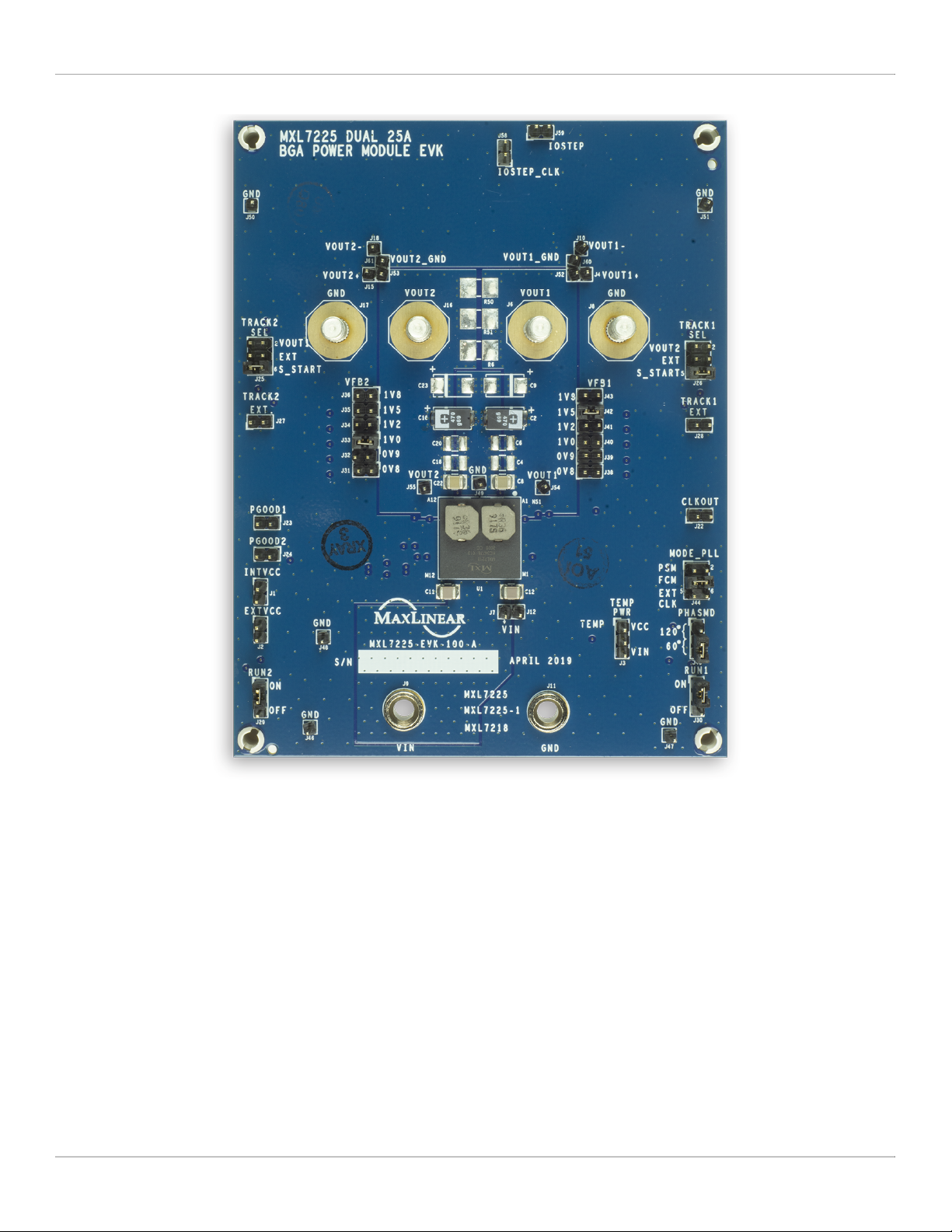
Quick EVB Set Up and Start Up
Factory Settings
In addition to utilizing the 4.5V to 15V input voltage range and dual 18A maximum load current rating capabilities of the
MxL7218 Power Module, the Evaluation Board has been set up with the factory default configurations shown below for
quick set up and operation. Do not exceed the EVB maximum load current rating.
The factory default configuration (Table 2) for the MxL7218 Evaluation Board is:
■VOUT1 = 1.5V ±1.5%
■VOUT2 = 1.0V ±1.5%
■500kHz Switching Frequency
■CCM mode. For other modes, see Jumper J44 MODE.
■Run is enabled for both channels. See Jumpers J30
RUN1 and J29 RUN2.
■Soft-start is selected for both channels. See Jumper
J26 TRACK1 SEL and Jumper J25 TRACK2 SEL.
■CLKOUT phase is 90 degrees, see Jumper J45
PHASMD.
Quick Start Up
To quickly see the regulator in operation:
1. Use the factory settings and default configuration. If
other settings or components are desired, apply them
before the next steps and see Set-Up Options for more.
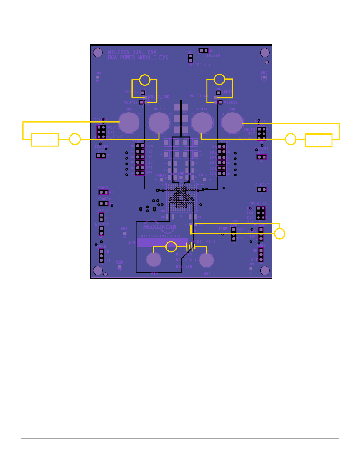
2. Connect a turned-off power supply that is within a VIN
specification of 4.5V to 15V, (12V typical) to VIN and
GND with short, thick leads. Use test pins VIN+ and
VIN- to monitor VIN and GND respectively. See
locations in Figure 1.
3. For the channel 1 output, connect an electronic load
initially set to 0A, that will be no more than the above
maximum IOUT (18A ), to VOUT1 and GND with short /
thick leads. Use test pins VOUT1 (J52) and
VOUT1_GND (J60) to monitor VOUT1 and GND
respectively. See locations in Figure 1.
4. For the channel 2 output, connect an electronic load
initially set to 0A, that will be no more than the above
maximum IOUT (18A ), to VOUT2 and GND with short,
thick leads. Use test pins VOUT2 (J53) and
VOUT2_GND (J61) to monitor VOUT2 and GND
respectively. See locations in Figure 1.
5. Turn on the power supply and check VOUT of both
channels. The EVB will power up and (factory default)
regulate the channel 1 output at 1.5V ±1.5% (1.4775V
to 1.5225V) and channel 2 output at 1.0V ±1.5%
(0.985V to 1.015V). Output ripple should bemeasured
across the output capacitors for each channel: C8 for
VOUT1 and C22 for VOUT2. The test points J52 and
J53 can be used to monitor the VOUT1 and VOUT2
outputs, respectively.
6. Set or vary the load (do not exceed the maximum IOUT)
and check VOUT and other desired performance levels
such as regulation and efficiency.
See Configuration and I/O Interfaces and Load Transient
Circuit for more on testing and monitoring. For Single Rail
Dual Phase 36A Operation and to vary VOUT see MxL7218
EVB Mode Selection.