MaxLinear MxL7704 Series User manual

Revision History
Revision Release Date Change Description
1A 2/28/18 Initial Release
MxL7704 EVB Manual Revision History
2/28/18 Rev 1A ii

Table of Contents
MxL7704 EVB Manual Table of Contents
2/28/18 iii
Introduction.................................................................................................................................1
Ordering Information..................................................................................................................1
Evaluation Board Overview.......................................................................................................2
System Set-Up .................................................................................................................................. 2
Powering Up the Evaluation Board................................................................................................. 3
Monitoring or Testing VOUT .......................................................................................................................................... 3
Typical Output Transient Response................................................................................................ 4
Pin Conguration .......................................................................................................................8
MxL7704-A-EVB Schematic.......................................................................................................9
MxL7704-X-EVB Schematic .....................................................................................................10
MxL7704 EVB PCB Layers....................................................................................................... 11
MxL7704 EVB Bill of Materials ................................................................................................17

List of Tables
MxL7704 EVB Manual List of Tables
iv2/28/18
Table 1: Evaluation Board Ordering Part Numbers ...................................................................... 1
Table 2: Factory Settings.............................................................................................................. 2
Table 3: MxL7704-A-EVB Bill of Materials.................................................................................. 13
Table 4: MxL7704-X-EVB Bill of Materials.................................................................................. 14

List of Figures
MxL7704 EVB Manual List of Figures
v2/28/18
Figure 1: Top View of MxL7704-A EVB ........................................................................................ 1
Figure 2: Top View of MxL7704-X EVB ........................................................................................ 1
Figure 3: Block Diagram MxL7704 EVB....................................................................................... 2
Figure 4: VIN Connection.............................................................................................................. 3
Figure 5: 3.3V Output Transient Response on Channel 1............................................................ 4
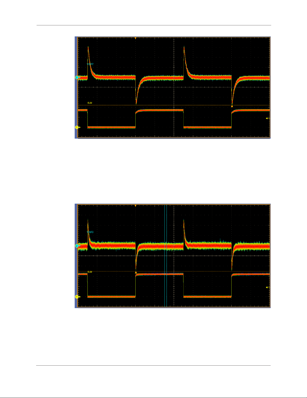
Figure 6: 1.8V Output Transient Response on Channel 2............................................................ 5
Figure 7: 1.35V Output Transient Response on Channel 3.......................................................... 5
Figure 8: MxL7704-AQB 1.2V Output Transient Response on Channel 4 ................................... 6
Figure 9: MxL7704-XQB 0.85V Output Transient Response on Channel 4 ................................. 6
Figure 10: MxL7704-AQB Power-Up Sequencing........................................................................ 7
Figure 11: MxL7704-AQB Power-Down Sequencing ................................................................... 7
Figure 12: MxL7704-XQB Power-Up Sequencing........................................................................ 7
Figure 13: MxL7704-XQB Power-Down Sequencing ................................................................... 7
Figure 14: Pin Conguration.........................................................................................................8
Figure 15: MxL7704-A-EVB Schematic........................................................................................ 9
Figure 16: MxL7704-X-EVB Schematic...................................................................................... 10
Figure 17: EVB PCB, Top View .................................................................................................. 11
Figure 18: EVB PCB Layer 2, Ground Plane..............................................................................12
Figure 19: EVB PCB Layer 3, Signal Plane................................................................................13
Figure 20: EVB PCB, Layer 4 Signal Plane................................................................................14
Figure 21: EVB PCB, Layer 5 Ground Planes............................................................................ 15
Figure 22: EVB PCB, Bottom View.............................................................................................16

MxL7704 EVB Manual
2/28/18 1
Introduction / Ordering Information
Introduction
The MxL7704 evaluation board provides a platform to evaluate the features and performance of the
MxL7704. The MxL7704 is a five output Universal PMIC optimized for powering low power FPGAs, DSPs,
and microprocessors from 5V inputs.
The MxL7704 power module and evaluation board come in two configurations which are summarized in
Table 1.
Please refer to the MxL7704 datasheet for additional information about the MxL7704.
Ordering Information
Table 1: Evaluation Board Ordering Part Numbers(1)
PMIC Evaluation Board Channel Output Voltage (V) Switching Frequency (MHz)
MxL7704-AQB-T MxL7704-A-EVB
VOUT1 3.3
1.5
VOUT2 1.8
VOUT3 1.35
VOUT4 1.2
MxL7704-XQB-T MxL7704-X-EVB
VOUT1 3.3
1
VOUT2 1.8
VOUT3 1.35
VOUT4 0.85
NOTE:
1. Refer to www.exar.com/MxL7704 for most up-to-date Ordering Information
Figure 1: Top View of MxL7704-A-EVB Figure 2: Top View of MxL7704-X-EVB

MxL7704 EVB Manual
2/28/18 2
Evaluation Board Overview
The block diagram shown in Figure 3 illustrates the connection points.
Figure 3: Block Diagram MxL7704 EVB
I2C
MxL7704
PGOOD
VOUT_LDO
SEQ EN
VOUT2
VOUT3 VOUT1
GLOBAL EN
ADC IN
VOUT4
VIN
System Set-Up
Jumpers are factory installed per Table 2 to configure the EVB for operation. Jumper and testing options
are described in the next sections. Refer to the product data sheet for additional information.
Table 2: Factory Settings
Jumper Factory Setting Description
Digi_Pwr to P5V J6, Jumper 1-2 Enables all pull-up resistors.
Overview / Set-Up

MxL7704 EVB Manual
2/28/18 3
Set Up
Powering Up the Evaluation Board
■Connect P2 (VIN+) and P3 (VIN-) to a 5V power supply. See Note A.
■Turn on the power supply. The EVB will power up and regulate the outputs as follows:
Channel 1: 3.3V
Channel 2: 1.8V
Channel 3: 1.35V
Channel 4: 1.2V (MXL7704-A-EVB) or 0.85V (MXL7704-X-EVB)
LDO: 3.3V
Monitoring or Testing VOUT
■The outputs may be left open or connected to an external load. A low impedance connection will
provide the best load regulation.
Figure 4: VIN Connection
Note A
Note A

MxL7704 EVB Manual
2/28/18 4
Figure 5: 3.3V Output Transient Response on Channel 1
Typical Output Transient Response
The following waveforms were captured on the MXL7704-A-EVB and MXL7704-X-EVB.
200µs / DIV
VIN = 5V, VOUT = 3.3V at 1A/µs Load Step
f = 1kHz
LOUT = 2.2µH
COUT = 22µF, 6.3V X5R Ceramic
COUT = 2 x 10µF, 6.3V X5R Ceramic
VOUT
80mV / DIV
IOUT
0.5A / DIV
Typical Transient Response

MxL7704 EVB Manual
2/28/18 5
Figure 7: 1.35V Output Transient Response on Channel 3
Figure 6: 1.8V Output Transient Response on Channel 2
200µs / DIV
VIN = 5V, VOUT = 1.8V at 1A/µs Load Step
f = 1kHz
LOUT = 1µH
COUT = 2 x 22µF, 6.3V X5R Ceramic
COUT = 10µF, 6.3V X5R Ceramic
VOUT
30mV / DIV
IOUT
0.5A / DIV
200µs / DIV
VIN = 5V, VOUT = 1.35V at 1A/µs Load Step
f = 1kHz
LOUT = 0.47µH
COUT = 2 x 22µF, 6.3V X5R Ceramic
VOUT
20mV / DIV
IOUT
0.5A / DIV
Typical Transient Response

MxL7704 EVB Manual
2/28/18 6
Figure 9: MxL7704-XQB 0.85V Output Transient Response on Channel 4
Figure 8: MxL7704-AQB 1.2V Output Transient Response on Channel 4
200µs / DIV
VIN = 5V, VOUT = 1.2V at 10A/µs Load Step
f = 1kHz
LOUT = 0.47µH
COUT = 3 x 47µF, 6.3V X5R Ceramic
VOUT
30mV / DIV
IOUT
0.5A / DIV
VOUT
20mV / DIV
IOUT
0.5A / DIV
200µs / DIV
VIN = 5V, VOUT = 0.85V at 10A/µs Load Step
f = 1kHz
LOUT = 0.47µH
COUT = 5 x 47µF, 6.3V X5R Ceramic
Typical Transient Response

MxL7704 EVB Manual
2/28/18 7
Figure 10: MxL7704-AQB Power-Up Sequencing
Figure 12: MxL7704-XQB Power-Up Sequencing
Figure 11: MxL7704-AQB Power-Down
Sequencing
Figure 13: MxL7704-XQB Power-Down
Sequencing
VOUT1LDO
VOUT2 VOUT3
VOUT4
VOUT1 LDO
VOUT2
VOUT3
VOUT4
VOUT1, LDO
VOUT2
VOUT3
VOUT4
VOUT1, LDO
VOUT2
VOUT3
VOUT4
Power Sequencing

MxL7704 EVB Manual
2/28/18 8
Pin Configuration
MxL7704
VOUT2
SDA
1
2
3
4
5
6
7
8
32 31 30 29 28 27 26 25
9 10 11 12 13 14 15 16
24
23
22
21
20
19
18
17
VDDIO
AGND
5VSYS
VOUT1
PG1
LDO
VIN
PGND2
LX2
LX4
LX4
SCL
VOUT4
AN0
AN1
PG2
PGND1
PGND4
PGND4
VOUT3
5VSYS
LX3
VIN1
LX1
SEQ EN
VIN3
VIN2
VIN4
LX4
GLOBAL EN
PAD PGND
Pin Conguration
Top View, 5mm x 5mm QFN-32
Figure 14: Pin Configuration

MxL7704 EVB Manual
2/28/18 9
EVB Schematic
MxL7704-A-EVB Schematic
Figure 15: MxL7704-A-EVB Schematic
SEQ EN
SCL
GLO EN
PG1
AN0
AN1
SEQ EN
PG1
GLO EN
PG2
PG2
SDA
Digi_Pwr
AGND
PGND
PGND
P5V
PGND
AGND
PGND
AGND
PGND
PGND
3.3V LDO
VOUT4
VOUT1
VOUT2
PGND
AGND
AGND
Digi_Pwr
AGND
AGND
PGND
PGND
AGNDAGND
AGND
AGND
AGND
AGND
AGND
VOUT3
PGND
AGND
AGND
AGND
AGND
P5V
PGND
P5V
PGND
VOUT1
PGND
VOUT2
PGND
VOUT3
PGND
VOUT4
PGND
3.3V LDO
AGND
AGND
P9
HDR_1x1
1
C11
DNP
0603
R6
0 Ohm
C24
DNP
C26
0.1uF
P6
HDR_1x1
1
C32
10uF
C6
22uF
0603
R19
4.7 Kohm
0603
R14
0 Ohm
1210
L1
2.2uH
0603
R15
4.7 Kohm
C37
0.1uF
MxL7704
U1
VDDIO
1
SDA
2
SCL
3
SEQ EN
4
PG1
5
GLOBAL EN
6
VIN
7
3.3V LDO
8
VOUT2
9
PGND2
10
LX2
11
VIN2
12
VIN4
13
LX4
14
LX4
15
LX4
16
PGND417
PGND418
VOUT4 19
PG2 20
AN1 21
AN0 22
AGND23
5VSYS 24
VOUT1 25
PGND126
LX1 27
VIN1 28
VIN3 29
LX3 30
5VSYS 31
VOUT3 32
EPAD 33
0603
R11
DNP
C33
10uF
C1
47uF
0603
R2
0 Ohm
C21
10uF
C14
0.1uF
C19
47uF
P13
HDR_1x1
1
J5
HEADER_1X3_2.54 mm_M
1
1
2
2
3
3
C35
DNP
0603
R10
0 Ohm
C15
1uF
P10
HDR_1x1
1
J2
HEADER_1X2_2.54 mm_M
1
2
P11
HDR_1x1
1
C2
10uF
0603
R8
0 Ohm
0603
R17
4.7 Kohm
C28
1uF
C20
22uF
1210
L4
0.47uH
0603
R20
4.7 Kohm
J1
HEADER_1X2_2.54 mm_M
1
2
Mini-USB-B
7
6
2
3
4
5
1
P8
HDR_1x1
1
0603
R13
DNP
1210
L3
0.47uH
C9
2.2uF
C36
0.1uF
0603
R4
0 Ohm
C30
10uF
C17
0.1uF
C29
10uF
P5
HDR_1x1
1
0603
R1
DNP
C31
DNP
C4
DNP
P7
HDR_1x1
1
0603
R9 10 Ohm
C7
DNP
0603
R5
0 Ohm
C10
1uF
C12
1uF
P2
HDR_1x1
1
J4
HEADER_1X3_2.54 mm_M
1
1
2
2
3
3
C8
22uF
C27
47uF
0603
R18
4.7 Kohm
P4
HDR_1x1
1
D1
SMBJ5.0A
1210
L2
1uH
0603
R16
4.7 Kohm
C22
10uF
0603
R12
0 Ohm
C3
47uF
0603
R7
0 Ohm
P12
HDR_1x1
1
J3
HEADER_1X3_2.54 mm_M
1
1
2
2
3
3
0603
R3
DNP
C25
10uF
C13
0.1uF
C23
47uF
J6
HEADER_1X3_2.54 mm_M
1
1
2
2
3
3
C34
DNP
C5
DNP
P3
HDR_1x1
1
PG1
SEQ EN
SCL
SDA
SCL
SEQ EN
GLO EN
PG1
SDA
GLO EN
P5V
P5V
AGNDAGND
PG2
PG2
AN1
AN0
P5V
AN0
PGND
VOUT2_FB
VOUT2_FB_R
VOUT3_FB
VOUT3_FB_R
VOUT1_FB_R
VOUT1_FB
VOUT4_FB_R
LX4LX4
LX2
LX3
LX1LX1
5VSYS5VSYS
P5V
P5V
5VSYS
AN1
3.3V LDO
VOUT4_FB
VOUT4_FB
SEQ EN
VOUT1_FB
VOUT2_FB
VOUT3_FB
Digi_Pwr
GLO EN
SDA
SCL
AN0
AN1
PG1
PG2
P5V
VOUT3
P5V
VOUT1
VOUT4
VOUT2

MxL7704 EVB Manual
2/28/18 10
MxL7704-X-EVB Schematic
SEQ EN
SCL
GLO EN
PG1
AN0
AN1
SEQ EN
PG1
GLO EN
PG2
PG2
SDA
Digi_Pwr
AGND
PGND
PGND
P5V
PGND
AGND
PGND
AGND
PGND
PGND
3.3V LDO
VOUT4
VOUT1
VOUT2
PGND
AGND
AGND
Digi_Pwr
AGND
AGND
PGND
PGND
AGNDAGND
AGND
AGND
AGND
AGND
AGND
VOUT3
PGND
AGND
AGND
AGND
AGND
P5V
PGND
P5V
PGND
VOUT1
PGND
VOUT2
PGND
VOUT3
PGND
VOUT4
PGND
3.3V LDO
AGND
AGND
P9
HDR_1x1
1
C11
DNP
0603
R6
0 Ohm
C24
DNP
C26
0.1uF
P6
HDR_1x1
1
C32
10uF
C6
22uF
0603
R19
4.7 Kohm
0603
R14
0 Ohm
1210
L1
2.2uH
0603
R15
4.7 Kohm
C37
0.1uF
MxL7704
U1
VDDIO
1
SDA
2
SCL
3
SEQ EN
4
PG1
5
GLOBAL EN
6
VIN
7
3.3V LDO
8
VOUT2
9
PGND2
10
LX2
11
VIN2
12
VIN4
13
LX4
14
LX4
15
LX4
16
PGND417
PGND418
VOUT4 19
PG2 20
AN1 21
AN0 22
AGND23
5VSYS 24
VOUT1 25
PGND126
LX1 27
VIN1 28
VIN3 29
LX3 30
5VSYS 31
VOUT3 32
EPAD 33
0603
R11
DNP
C33
10uF
C1
47uF
0603
R2
0 Ohm
C21
10uF
C14
0.1uF
C19
47uF
P13
HDR_1x1
1
J5
HEADER_1X3_2.54 mm_M
1
1
2
2
3
3
C35
DNP
0603
R10
0 Ohm
C15
1uF
P10
HDR_1x1
1
J2
HEADER_1X2_2.54 mm_M
1
2
P11
HDR_1x1
1
C2
10uF
0603
R8
0 Ohm
0603
R17
4.7 Kohm
C28
1uF
C20
22uF
1210
L4
0.47uH
0603
R20
4.7 Kohm
J1
HEADER_1X2_2.54 mm_M
1
2
Mini-USB-B
7
6
2
3
4
5
1
P8
HDR_1x1
1
0603
R13
DNP
1210
L3
1uH
C9
2.2uF
C36
0.1uF
0603
R4
0 Ohm
C30
10uF
C17
0.1uF
C29
10uF
P5
HDR_1x1
1
0603
R1
DNP
C31
47uF
C4
DNP
P7
HDR_1x1
1
0603
R9 10 Ohm
C7
DNP
0603
R5
0 Ohm
C10
1uF
C12
1uF
P2
HDR_1x1
1
J4
HEADER_1X3_2.54 mm_M
1
1
2
2
3
3
C8
22uF
C27
47uF
0603
R18
4.7 Kohm
P4
HDR_1x1
1
D1
SMBJ5.0A
1210
L2
2.2uH
0603
R16
4.7 Kohm
C22
10uF
0603
R12
0 Ohm
C3
47uF
0603
R7
0 Ohm
P12
HDR_1x1
1
J3
HEADER_1X3_2.54 mm_M
1
1
2
2
3
3
0603
R3
DNP
C25
10uF
C13
0.1uF
C23
47uF
J6
HEADER_1X3_2.54 mm_M
1
1
2
2
3
3
C34
47uF
C5
DNP
P3
HDR_1x1
1
PG1
SEQ EN
SCL
SDA
SCL
SEQ EN
GLO EN
PG1
SDA
GLO EN
P5V
P5V
AGNDAGND
PG2
PG2
AN1
AN0
P5V
AN0
PGND
VOUT2_FB
VOUT2_FB_R
VOUT3_FB
VOUT3_FB_R
VOUT1_FB_R
VOUT1_FB
VOUT4_FB_R
LX4LX4
LX2
LX3
LX1LX1
VOUT3
5VSYS5VSYS
P5V
P5V
5VSYS
AN1
3.3V LDO
VOUT4_FB
VOUT4_FB
SEQ EN
VOUT1_FB
VOUT2_FB
VOUT3_FB
Digi_Pwr
GLO EN
SDA
SCL
AN0
AN1
PG1
PG2
P5V
P5V
VOUT1
VOUT2
VOUT4
Figure 16: MxL7704-X-EVB Schematic
EVB Schematic

MxL7704 EVB Manual
2/28/18 11
MxL7704 EVB PCB Layers
PCB
Figure 17: EVB PCB, Top View

MxL7704 EVB Manual
2/28/18 12
Figure 18: EVB PCB Layer 2, Ground Plane
PCB

MxL7704 EVB Manual
2/28/18 13
Figure 19: EVB PCB Layer 3, Signal Plane
PCB

MxL7704 EVB Manual
2/28/18 14
PCB
Figure 20: EVB PCB, Layer 4 Signal Plane

MxL7704 EVB Manual
2/28/18 15
Figure 21: EVB PCB, Layer 5 Ground Planes
PCB
This manual suits for next models
2
Table of contents
Other MaxLinear Motherboard manuals

MaxLinear
MaxLinear XR31234 User manual

MaxLinear
MaxLinear XR32220 User manual

MaxLinear
MaxLinear MxL7225 User manual

MaxLinear
MaxLinear MxL7218-EVK-2 User manual

MaxLinear
MaxLinear XR17V354 User manual

MaxLinear
MaxLinear XR77XXEVB-XCM-V80 User manual

MaxLinear
MaxLinear MxL7225 User manual

MaxLinear
MaxLinear MxL7213 User manual

MaxLinear
MaxLinear MxL7218 User manual