MaxLinear MxL7225 User manual

Quad MxL7225 200A Multiphase EVK User Manual Revision History
12/7/20 021UMR01 ii
Revision History
Document No. Release Date Change Description
021UMR01 12/7/20 Initial Release

Quad MxL7225 200A Multiphase EVK User Manual Table of Contents
12/7/20 021UMR01 iii
Table of Contents
Introduction......................................................................................................................................................... 1
Quick EVK Set Up and Start Up....................................................................................................................................1
Factory Settings ...................................................................................................................................................1
Quick Start Up ......................................................................................................................................................1
Reference Documentation ................................................................................................................................. 3
Ordering Information.......................................................................................................................................... 3
Evaluation Board Overview ............................................................................................................................... 4
Configuration and I/O Interfaces ....................................................................................................................... 5
EXT_CLK, Jumper JP1 .................................................................................................................................................5
RUN, Jumper JP2 .........................................................................................................................................................5
TRACK_CONTROL.......................................................................................................................................................5
PGOOD .........................................................................................................................................................................5
EXTVCC........................................................................................................................................................................5
EXT PULSE...................................................................................................................................................................5
Set-Up Options.................................................................................................................................................... 6
Jumper JP1 CLK ...........................................................................................................................................................6
Jumper JP2 RUN ..........................................................................................................................................................6
Jumpers JP4 - JP8 VOUT SELECT ..............................................................................................................................6
Test Interfaces..................................................................................................................................................... 7
Load Transient Circuit ...................................................................................................................................................7
Performance........................................................................................................................................................ 8
Efficiency .......................................................................................................................................................................8
Load Transient Response .............................................................................................................................................8
Output Ripple ................................................................................................................................................................9
Thermal .........................................................................................................................................................................9
Quad MxL7225 EVK Schematic....................................................................................................................... 10
Quad MxL7225 EVK PCB Layers..................................................................................................................... 14
Quad MxL7225 EVK Bill of Materials .............................................................................................................. 19

Quad MxL7225 200A Multiphase EVK User Manual List of Figures
12/7/20 021UMR01 iv
List of Figures
Figure 1: Monitoring VIN and VOUT.........................................................................................................................................2
Figure 2: Top View of MxL7225 200A Multiphase EVK..........................................................................................................3
Figure 3: Quad MxL7225 200A Multiphase EVK Block Diagram ...........................................................................................4
Figure 4: Load Transient Circuit .............................................................................................................................................7
Figure 5: Measured Efficiency (VIN = 12V, fSW = 500kHz) .....................................................................................................8
Figure 6: Load Transient Response, 100A to 150A (VIN = 12V, VOUT = 1V, fSW = 500kHz) .................................................8
Figure 7: Measured Output Voltage Ripple (VIN = 12V, VOUT = 1V, Load = 200A, fSW = 500kHz)........................................9
Figure 8: Thermal Capture (VIN = 12V, VOUT = 1V, Load = 200A, fSW = 500kHz, 400LFM)..................................................9
Figure 9: EVK Schematic .....................................................................................................................................................10
Figure 10: EVK Schematic, Continued .................................................................................................................................11
Figure 11: EVK Schematic, Continued .................................................................................................................................12
Figure 12: EVK Schematic, Continued .................................................................................................................................13
Figure 13: EVK PCB Silkscreen Top ....................................................................................................................................14
Figure 14: EVK PCB Layer 1................................................................................................................................................14
Figure 15: EVK PCB Layer 2................................................................................................................................................15
Figure 16: EVK PCB Layer 3................................................................................................................................................15
Figure 17: EVK PCB Layer 4................................................................................................................................................16
Figure 18: EVK PCB Layer 5................................................................................................................................................16
Figure 19: EVK PCB Layer 6................................................................................................................................................17
Figure 20: EVK PCB Layer 7................................................................................................................................................17
Figure 21: EVK PCB Layer 8................................................................................................................................................18

Quad MxL7225 200A Multiphase EVK User Manual List of Tables
12/7/20 021UMR01 v
List of Tables
Table 1: Evaluation Board Ordering Part Number ................................................................................................ 3
Table 2: Factory Settings...................................................................................................................................... 6
Table 3: JP1 Options ............................................................................................................................................ 6
Table 4: JP2 Options ............................................................................................................................................ 6
Table 5: JP4 - JP8 Options................................................................................................................................... 6
Table 6: EVK Bill of Materials ............................................................................................................................. 19

Quad MxL7225 200A Multiphase EVK User Manual Introduction
12/7/20 021UMR01 1
Introduction
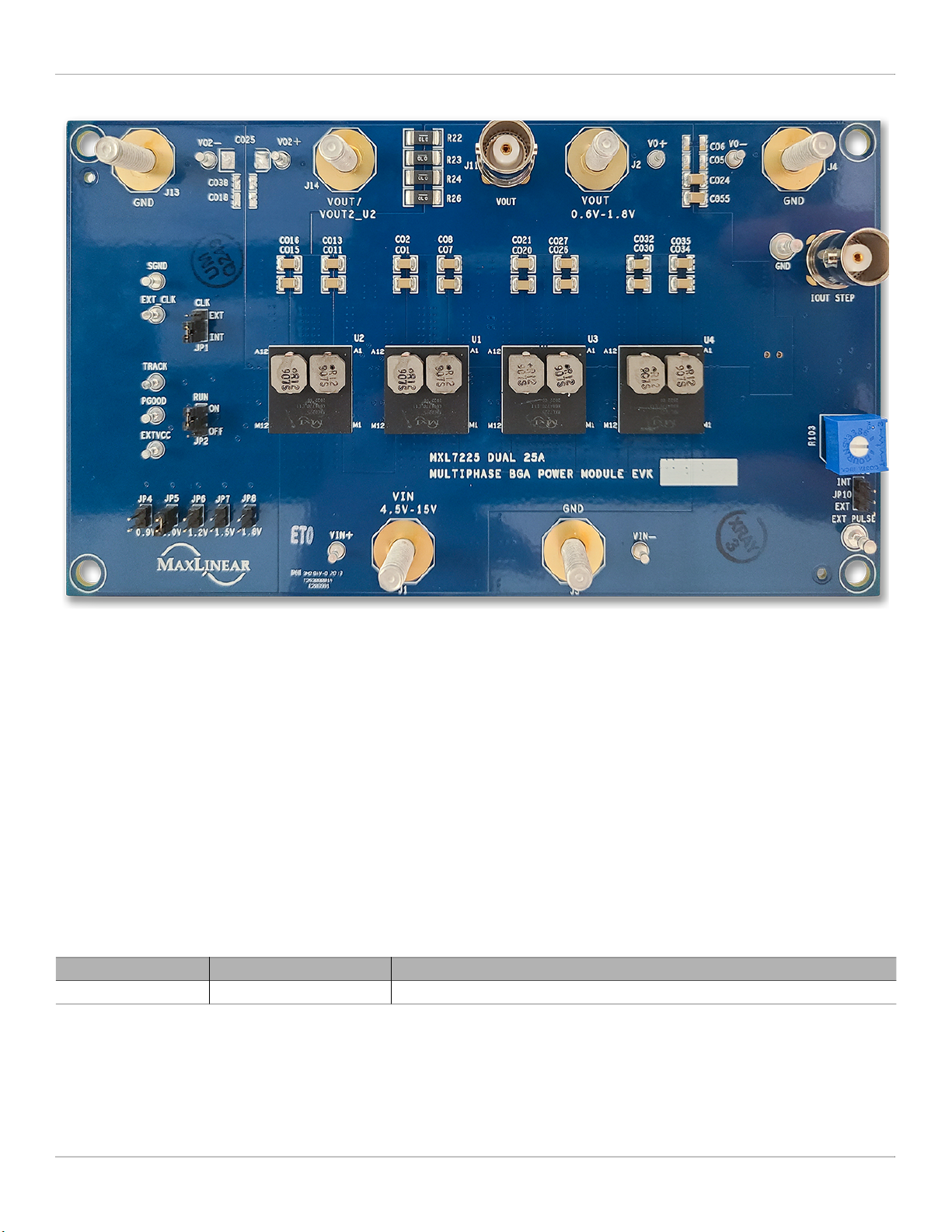
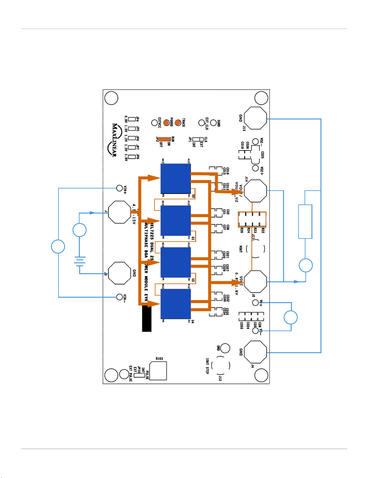
The Quad MxL7225 200A Multiphase Evaluation Board provides a platform to evaluate the features and performance of
four MxL7225 Power Modules connected in parallel to supply up to a 200A load. Each MxL7225 is a dual 25A Power
Module which are optimized for powering Telecom, Networking and Industrial equipment. This manual covers both the BGA
and LGA evaluation boards versions of this 200A multiphase application.
Quick EVK Set Up and Start Up
Factory Settings
In addition to utilizing the 4.5V to 15V input voltage range of the MxL7225’s and the 200A maximum load current rating
capabilities of using the four MxL7225 Power Modules together, the evaluation board has been set up with the factory
default configurations shown below for quick set up and operation. Do not exceed the EVK maximum load current
rating.
The factory default configuration (Table 2) for the Quad MxL7225 Evaluation Board is:
■VIN = 4.5V to 15V
■VOUT = 1.0V ±1.5%. For other VOUT see Jumpers JP4 -
JP8 VOUT SELECT.
■IOUT = 0A to 200A
■500kHz switching frequency
■Run is enabled for both channels of all 4 of the
MxL7225’s (all 8 channels). See RUN, Jumper JP2.
■Continuous current mode using internal clock. To use
an external clock, see EXT_CLK, Jumper JP1
■One pin output voltage ramp up and down tracking
programmability
■A 6.5ms soft-start is selected for all channels
■Sensing diode biasing at 100µA for internal
temperature sense
Quick Start Up
To quickly see the regulator in operation:
1. Use the factory settings and default configuration. If
other settings or components are desired, apply them
before the next steps and see Set-Up Options for more.
2. With a power supply turned off and within a VIN
specification of 4.5V to 15V (12V typical), connect it to
VIN and GND with short, thick leads. Use test pins
VIN+ and VIN- to monitor VIN and GND respectively.
See locations in Figure 1.
3. For the output, connect a meter and electronic load
initially set to 0A, that will be no more than the above
maximum IOUT (200A ), to VOUT and GND with short /
thick leads capable of this current. See setup and
locations in Figure 1.
4. Turn on the power supply and check VOUT. Check to
make sure that JP2 is on the ON position. The EVK will
power up and (factory default) regulate the output at 1V
±1.5% (0.985V to 1.015V).
5. Set or vary the load (do not exceed the maximum IOUT)
and check VOUT and other desired performance levels
such as regulation and efficiency.
See Configuration and I/O Interfaces and Load Transient
Circuit for more on testing and monitoring.

Quad MxL7225 200A Multiphase EVK User Manual Quick EVK Set Up and Start Up
12/7/20 021UMR01 2
Figure 1: Monitoring VIN and VOUT
VOUT
A
Load V
+-
V
+-
A+-
VIN

Quad MxL7225 200A Multiphase EVK User Manual Reference Documentation
12/7/20 021UMR01 3
Figure 2: Top View of MxL7225 200A Multiphase EVK
Reference Documentation
Please refer to the MxL7225 Data Sheet for additional information about the MxL7225. The datasheet includes a full list of
IC features, pinout, pin descriptions, typical performance characteristics and external component calculations. This manual
is meant to be used in conjunction with the datasheet.
This manual provides Quad MxL7225 EVK Schematic, Quad MxL7225 EVK PCB Layers and Quad MxL7225 EVK Bill of
Materials that can be utilized to assist in your board design. The schematics are also available on the MxL7225 product
page.
Ordering Information
1. Refer to www.maxlinear.com/MxL7225 for most up-to-date Ordering Information.
Table 1: Evaluation Board Ordering Part Number(1)
Power Module Evaluation Board Description
MxL7225-ABA-T MxL7225-EVK-2 Quad MxL7225 BGA Power Module Multiphase EVK

Quad MxL7225 200A Multiphase EVK User Manual Evaluation Board Overview
12/7/20 021UMR01 4
Evaluation Board Overview
The block diagram shown in Figure 3 illustrates the 7 MxL7225 channels connected in parallel with the 8th channel as the
master and the connection points for VIN, VOUT, and VOUT2. Also represented are the CLKOUT to MODE_PLLIN
connections between the 4 MxL7225 ICs.
VOUT and VOUT2 connected via R22, R23, R24 and R26
VFB of all 8 channels connected
RUN of all 8 channels connected and connected to JP2
TRACK of all 8 channels connected and connected to TRACK_CONTROL point on board
PGOOD of all 8 channels (with pullups) connected and connected to PGOOD point on board
Figure 3: Quad MxL7225 200A Multiphase EVK Block Diagram
A
A
V
V
+ -
+ -
+ -
VIN
Load VOUT
VIN
VOUT
VOUT2
MxL7225
MxL7225
MxL7225
MxL7225
0 - 200A

Quad MxL7225 200A Multiphase EVK User Manual Configuration and I/O Interfaces
12/7/20 021UMR01 5
Configuration and I/O Interfaces
EXT_CLK, Jumper JP1
Jumper J1 provides an option to connect and synchronize to an external clock or use an internal clock (default). See
EXT_CLK, Jumper JP1.
RUN, Jumper JP2
Jumper JP2 enables (ON) or disables (OFF) all 8 channels. See RUN, Jumper JP2.
TRACK_CONTROL
The board’s output voltage tracks the voltage on the TRACK_CONTROL test point when applied.
PGOOD
A PGOOD test point is provided for all 8 channels. PGOOD signals are tied to INTVCC through 10kΩ resistors.
EXTVCC
A connection point is provided to inject EXTVCC, if desired.
EXT PULSE
Used to test load transients. See Load Transient Circuit.

Quad MxL7225 200A Multiphase EVK User Manual Set-Up Options
12/7/20 021UMR01 6
Set-Up Options
Jumpers are factory installed per Table 2 to configure the EVK for operation. Jumper and testing options are described in
the next sections. Refer to the product datasheet for additional information.
Jumper JP1 CLK
Jumper JP2 RUN
Jumpers JP4 - JP8 VOUT SELECT
Table 5: JP4 - JP8 Options
Table 2: Factory Settings
Jumper Label Factory Setting Description
JP1 CLK Jumper 2-3 Internal clock
JP2 RUN Jumper 1-2 On
VOUT SELECT
JP4 0.9V No Jumper
VOUT = 1.0V selected
JP5 1.0V Jumper 1-2
JP6 1.2V No Jumper
JP7 1.5V No Jumper
JP8 1.8V No Jumper
Table 3: JP1 Options
Jumper Options Description
Jumper 1-2 External clock may be applied to synchronize to.
Jumper 2-3 (default) Internal clock.
Table 4: JP2 Options
Jumper Options Description
Jumper 1-2 (default) On, all channels are enabled.
Jumper 2-3 Off, all channels are disabled.
Jumper Jumper Options Description
JP4 Jumper 1-2 VOUT = 0.9V selected only.
No jumper (default) VOUT = 0.9V not selected.
JP5 Jumper 1-2 (default) VOUT = 1.0V selected only.
No jumper VOUT = 1.0V not selected.
JP6 Jumper 1-2 VOUT = 1.2V selected only.
No jumper (default) VOUT = 1.2V not selected.
JP7 Jumper 1-2 VOUT = 1.5V selected only.
No jumper (default) VOUT = 1.5V not selected.
JP8 Jumper 1-2 VOUT = 1.8V selected only.
No jumper (default) VOUT = 1.8V not selected.

Quad MxL7225 200A Multiphase EVK User Manual Test Interfaces
12/7/20 021UMR01 7
Test Interfaces
Load Transient Circuit
A load transient circuit is provided to allow optional testing of load transients. The EXT PULSE (E33) clock input is used to
drive the transient signal. The load step generated by the FETs (Q1 and Q2) is very fast; the step slew rate is >40A/µs for a
50A transient load test case.
To measure load transient response, use the circuit shown in Figure 4. Populate R101 and R102 and apply a small duty
cycle pulse signal to the EXT PULSE (E33) input (~ 1%). Adjust the amplitude of the EXT PULSE (E33) pulse to set the
load current. Start at a pulse amplitude of 2V and increase while monitoring the IOUT STEP (J12) voltage. The load current
at IOUT STEP (J12) is 5mV/A. For an example, a 100A load will occur when a 500mV pulse is observed at J12.
Figure 4: Load Transient Circuit
9287
38/6(
'<1$0,&/2$'&,5&8,7
+]'XW\&\FOH
,17 (;7
,28767(3
9
9287
5
N
5
4
68'103(* -
4
68'103(*
&
X)
9
5
.
5
.
5 2KP
&
Q)
&
X)
9
5
.
&
X)
&
X)
&287
X)
5
.
5
5
&
X)
9
5
.
5
5
&
S)
-3
&
X)
9
5
8 /7,6
9287
9
,1
,1
9
(
*1'
-
5 0
5
.
&
X)
9
(
(;738/6(
8 /7&,6
02'
*1'
6(7
',9
9
287
&
X)
9

Quad MxL7225 200A Multiphase EVK User Manual Performance
12/7/20 021UMR01 8
Performance
Efficiency
Figure 5: Measured Efficiency (VIN = 12V, fSW = 500kHz)
Load Transient Response
Figure 6: Load Transient Response, 100A to 150A (VIN = 12V, VOUT = 1V, fSW = 500kHz)
60
70
80
90
100
0 20 40 60 80 100 120 140 160 180 200
Efficiency (%)
Load Current (A)
V
OUT
= 1.5V
V
OUT
= 1.0V
20mV/DIV, AC Coupled
(20MHz BW)
100A to 150A Load

Quad MxL7225 200A Multiphase EVK User Manual Output Ripple
12/7/20 021UMR01 9
Output Ripple
2. 200A load on J7 with standard demo circuit default setup.
Figure 7: Measured Output Voltage Ripple (VIN = 12V, VOUT = 1V, Load = 200A, fSW = 500kHz)
Thermal
3. Ambient temperature = 23.3°C, airflow = 400LFM, no heat sink.
Figure 8: Thermal Capture (VIN = 12V, VOUT = 1V, Load = 200A, fSW = 500kHz, 400LFM)
5mV/DIV
(20MHz BW)

Quad MxL7225 200A Multiphase EVK User Manual Quad MxL7225 EVK Schematic
12/7/20 021UMR01 10
Quad MxL7225 EVK Schematic
Figure 9: EVK Schematic
' '
& &
% %
$ $
9)%
&203
&/.287B8
581
75$&.
3*22'
,179&&B8
9287
9287
9,1
(;79&&
,179&&B8
92
92
9287
7LWOH
6L]H 'RFXPHQW1XPEHU 5HY
'DWH 6KHHW RI
'UDZ
5LQFRQ&LUFOH
6DQ-RVH&$
$
0[/(9.6FKHPDWLF
&
)ULGD\ )HEUXDU\
)&RVWHVFX
0[/(9.$
7LWOH
6L]H 'RFXPHQW1XPEHU 5HY
'DWH 6KHHW RI
'UDZ
5LQFRQ&LUFOH
6DQ-RVH&$
$
0[/(9.6FKHPDWLF
&
)ULGD\ )HEUXDU\
)&RVWHVFX
0[/(9.$
7LWOH
6L]H 'RFXPHQW1XPEHU 5HY
'DWH 6KHHW RI
'UDZ
5LQFRQ&LUFOH
6DQ-RVH&$
$
0[/(9.6FKHPDWLF
&
)ULGD\ )HEUXDU\
)&RVWHVFX
0[/(9.$
&,1
9
( 6:
5
237
&2
237
&2
9
&,1
9
&,1
9
&2
9
&
237
&2
237
&2
9
&
X)
9
5
237
&2
X)
9
&2
9
5
2KP
5
.
&
X)
9
8
0;/B%*$
9287B
$
9287B
$
9287B
$
9287B
$
9287B
$
9287B
%
9287B
%
9287B
%
9287B
%
9287B
%
9287B
&
9287B
&
9287B
&
9287B
&
9)%
'
6:
*
3*22'
*
&203
(
581
)
75$&.
(
92876
&
9287B
$
9287B
$
9287B
$
9287B
$
9287B
$
9287B
%
9287B
%
9287B
%
9287B
%
9287B
%
9287B
&
9287B
&
9287B
&
9287B
&
9)%
'
6:
*
3*22'
*
&203
(
581
)
75$&.
'
92876
&
9,1B
0
9,1B
0
9,1B
0
9,1B
0
9,1B
0
9,1B
0
9,1B
0
9,1B
0
9,1B
0
9,1B
0
9,1B
/
9,1B
/
9,1B
/
9,1B
/
9,1B
/
9,1B
/
9,1B
/
9,1B
/
9,1B
/
9,1B
/
9,1B
.
9,1B
.
9,1B
.
9,1B
.
9,1B
.
9,1B
.
9,1B
-
9,1B
-
9,1B
-
9,1B
-
9,1B
-
9,1B
-
*1'B
$
*1'B
$
*1'B
%
*1'B
%
*1'B
'
*1'B
'
*1'B
'
*1'B
'
*1'B
'
*1'B
'
*1'B
'
*1'B
'
*1'B
(
*1'B
(
*1'B
(
*1'B
(
*1'B
(
*1'B
(
*1'B
(
*1'B
)
*1'B
)
*1'B
)
*1'B
)
*1'B
)
*1'B
)
*1'B
*
*1'B
*
*1'B
*
*1'B
*
*1'B
+
*1'B
+
*1'B
+
*1'B
+
*1'B
+
*1'B
+
*1'B
+
*1'B
+
*1'B
+
*1'B
+
*1'B
+
*1'B
0
*1'B
0
*1'B
/
*1'B
-
*1'B
-
*1'B
-
*1'B
-
*1'B
.
*1'B
.
*1'B
.
*1'B
.
*1'B
.
*1'B
.
*1'B
/
6*1'B
&
6*1'B
'
6*1'B
)
6*1'B
)
6*1'B
*
6*1'B
*
)6(7
&
3+$60'
*
',))3
(
',))1
(
&/.287
*
02'(3//,1
)
7(03
-
,179&&
+
(;79&&
-
',))287
)
&
237
5
237
&2
237
&,1
9
5
237
&2
237
5
237
&
237
&2
9
&2
9
( 9RXW &2
X)
9
&2
9
5
.
(
6:
5
237 ( 9RXW
&2
9
&
237
&203
581
&203
75$&.
9)%
3*22'
581
9)%
75$&.
3*22'
&/.287B8

Quad MxL7225 200A Multiphase EVK User Manual Quad MxL7225 EVK Schematic
12/7/20 021UMR01 11
Figure 10: EVK Schematic, Continued
' '
& &
% %
$ $
&203
&/.287B8
&/.287B8
581
9)%
3*22'
75$&.
9287
,179&&B8
9287
9,1
(;79&&
,179&&B8
,179&&B8
7LWOH
6L]H 'RFXPHQW1XPEHU 5HY
'DWH 6KHHW RI
'UDZ
5LQFRQ&LUFOH
6DQ-RVH&$
$
0[/(9.6FKHPDWLF
&
6XQGD\)HEUXDU \
)&RVWHVFX
0[/(9.$
7LWOH
6L]H 'RFXPHQW1XPEHU 5HY
'DWH 6KHHW RI
'UDZ
5LQFRQ&LUFOH
6DQ-RVH&$
$
0[/(9.6FKHPDWLF
&
6XQGD\)HEUXDU \
)&RVWHVFX
0[/(9.$
7LWOH
6L]H 'RFXPHQW1XPEHU 5HY
'DWH 6KHHW RI
'UDZ
5LQFRQ&LUFOH
6DQ-RVH&$
$
0[/(9.6FKHPDWLF
&
6XQGD\)HEUXDU \
)&RVWHVFX
0[/(9.$
&
237
&,1
9
&2
237
8
0;/B%*$
9287B
$
9287B
$
9287B
$
9287B
$
9287B
$
9287B
%
9287B
%
9287B
%
9287B
%
9287B
%
9287B
&
9287B
&
9287B
&
9287B
&
9)%
'
6:
*
3*22'
*
&203
(
581
)
75$&.
(
92876
&
9287B
$
9287B
$
9287B
$
9287B
$
9287B
$
9287B
%
9287B
%
9287B
%
9287B
%
9287B
%
9287B
&
9287B
&
9287B
&
9287B
&
9)%
'
6:
*
3*22'
*
&203
(
581
)
75$&.
'
92876
&
9,1B
0
9,1B
0
9,1B
0
9,1B
0
9,1B
0
9,1B
0
9,1B
0
9,1B
0
9,1B
0
9,1B
0
9,1B
/
9,1B
/
9,1B
/
9,1B
/
9,1B
/
9,1B
/
9,1B
/
9,1B
/
9,1B
/
9,1B
/
9,1B
.
9,1B
.
9,1B
.
9,1B
.
9,1B
.
9,1B
.
9,1B
-
9,1B
-
9,1B
-
9,1B
-
9,1B
-
9,1B
-
*1'B
$
*1'B
$
*1'B
%
*1'B
%
*1'B
'
*1'B
'
*1'B
'
*1'B
'
*1'B
'
*1'B
'
*1'B
'
*1'B
'
*1'B
(
*1'B
(
*1'B
(
*1'B
(
*1'B
(
*1'B
(
*1'B
(
*1'B
)
*1'B
)
*1'B
)
*1'B
)
*1'B
)
*1'B
)
*1'B
*
*1'B
*
*1'B
*
*1'B
*
*1'B
+
*1'B
+
*1'B
+
*1'B
+
*1'B
+
*1'B
+
*1'B
+
*1'B
+
*1'B
+
*1'B
+
*1'B
+
*1'B
0
*1'B
0
*1'B
/
*1'B
-
*1'B
-
*1'B
-
*1'B
-
*1'B
.
*1'B
.
*1'B
.
*1'B
.
*1'B
.
*1'B
.
*1'B
/
6*1'B
&
6*1'B
'
6*1'B
)
6*1'B
)
6*1'B
*
6*1'B
*
)6(7
&
3+$60'
*
',))3
(
',))1
(
&/.287
*
02'(3//,1
)
7(03
-
,179&&
+
(;79&&
-
',))287
)
&2
9
&,1
9
&2
9
&,1
9
&
X)
9
&
237
( 6:
&2
237
( 9RXW
( 9RXW
&2
9
&2
9
&2
9
&
X)
9
5
237
5
.
5
.
5
.
&2
237
&2
9
5
237
&2
237
&2
X)
9
&2
9
&,1
9
&2
X)
9
&2
9
9
&,1
X)
9
5
2KP
ϭϲ
6:
&203
581
&203
&/.287B8
&/.287B8
3*22'
581
9)%
75$&.
3*22'
75$&.
9)%

Quad MxL7225 200A Multiphase EVK User Manual Quad MxL7225 EVK Schematic
12/7/20 021UMR01 12
Figure 11: EVK Schematic, Continued
' '
& &
% %
$ $
5(029(2+0-803(56
)256(3$5$7(9287B8
&203
&/.287B8
&/.287B8
581
75$&.
3*22'
9)%
9287
,179&&B8
9287B8
9,1
(;79&&
,179&&B8
92
92
92 92
,179&&B8
92
9287B89287
9287B8
7LWOH
6L]H 'RFXPHQW1XPEHU 5HY
'DWH 6KHHW RI
'UDZ
5LQFRQ&LUFOH
6DQ-RVH&$
$
0[/(9.6FKHPDWLF
&
)ULGD\ )HEUXDU\
)&RVWHVFX
0[/(9.$
7LWOH
6L]H 'RFXPHQW1XPEHU 5HY
'DWH 6KHHW RI
'UDZ
5LQFRQ&LUFOH
6DQ-RVH&$
$
0[/(9.6FKHPDWLF
&
)ULGD\ )HEUXDU\
)&RVWHVFX
0[/(9.$
7LWOH
6L]H 'RFXPHQW1XPEHU 5HY
'DWH 6KHHW RI
'UDZ
5LQFRQ&LUFOH
6DQ-RVH&$
$
0[/(9.6FKHPDWLF
&
)ULGD\ )HEUXDU\
)&RVWHVFX
0[/(9.$
&2
X)
9
5
&2
237
&
X)
9
5
2KP
5
237
5
2KP
&
237
5
2KP
&
X)
9
&2
237
-
*1'
8
0;/B%*$
9287B
$
9287B
$
9287B
$
9287B
$
9287B
$
9287B
%
9287B
%
9287B
%
9287B
%
9287B
%
9287B
&
9287B
&
9287B
&
9287B
&
9)%
'
6:
*
3*22'
*
&203
(
581
)
75$&.
(
92876
&
9287B
$
9287B
$
9287B
$
9287B
$
9287B
$
9287B
%
9287B
%
9287B
%
9287B
%
9287B
%
9287B
&
9287B
&
9287B
&
9287B
&
9)%
'
6:
*
3*22'
*
&203
(
581
)
75$&.
'
92876
&
9,1B
0
9,1B
0
9,1B
0
9,1B
0
9,1B
0
9,1B
0
9,1B
0
9,1B
0
9,1B
0
9,1B
0
9,1B
/
9,1B
/
9,1B
/
9,1B
/
9,1B
/
9,1B
/
9,1B
/
9,1B
/
9,1B
/
9,1B
/
9,1B
.
9,1B
.
9,1B
.
9,1B
.
9,1B
.
9,1B
.
9,1B
-
9,1B
-
9,1B
-
9,1B
-
9,1B
-
9,1B
-
*1'B
$
*1'B
$
*1'B
%
*1'B
%
*1'B
'
*1'B
'
*1'B
'
*1'B
'
*1'B
'
*1'B
'
*1'B
'
*1'B
'
*1'B
(
*1'B
(
*1'B
(
*1'B
(
*1'B
(
*1'B
(
*1'B
(
*1'B
)
*1'B
)
*1'B
)
*1'B
)
*1'B
)
*1'B
)
*1'B
*
*1'B
*
*1'B
*
*1'B
*
*1'B
+
*1'B
+
*1'B
+
*1'B
+
*1'B
+
*1'B
+
*1'B
+
*1'B
+
*1'B
+
*1'B
+
*1'B
+
*1'B
0
*1'B
0
*1'B
/
*1'B
-
*1'B
-
*1'B
-
*1'B
-
*1'B
.
*1'B
.
*1'B
.
*1'B
.
*1'B
.
*1'B
.
*1'B
/
6*1'B
&
6*1'B
'
6*1'B
)
6*1'B
)
6*1'B
*
6*1'B
*
)6(7
&
3+$60'
*
',))3
(
',))1
(
&/.287
*
02'(3//,1
)
7(03
-
,179&&
+
(;79&&
-
',))287
)
(
92
( 6:
5
.
&2
237
&2
237
&,1
X)
9
&2
237
5
2KP
5
2KP
5
2KP
(
6:
&2
237
(
9RXW
5
237
5
.
&,1
X)
9
&2
X)
9
5
237
5
2KP
&
237
-
9287B8
9287
&2
X)
9
&2
X)
9
&2
237
( 9RXW
&
237
&
237
&
237
(
92
5
.
5
2KP
&,1
X)
9
&2
237
9
&2
237
5
237
5
2KP
5
2KP
&
237
&2
X)
9
&2
237
9
5
237
&
237
&2
X)
9
&,1
X)
9
5
5
&2
237
5
2KP
&203B8
581B8
&203
75$&.B8
9)%
3*22'
581
75$&.
3*22'B8
',))287B8
',))287B8
9)%B8
3*22'B8
9)%B8
581B8
&203B8
75$&.B8

Quad MxL7225 200A Multiphase EVK User Manual Quad MxL7225 EVK Schematic
12/7/20 021UMR01 13
Figure 12: EVK Schematic, Continued
' '
& &
% %
$ $
9287
6(/(&7
EKdhE>^^Kd,Zt/^^W/&/
ϭ>>W/dKZ^Z^/^dKZ^ϬϲϬϯ
^^z ,&
Ͳ hϭhϮ
hϭhϮhϯ
hϭhϮhϯhϰ
Ͳ
Ͳ
ϭϬϬ
ϭϱϬ
ϮϬϬ
,RXW
KWd
Ϭ
KWd
Zϭϯ
KWd
Ϭ
Ϭ
Zϯϰ
KWd
ϮϮƵ&
ϮϮƵ&
&LQ
KWd
KWd
ϮϮƵ&
&LQ
KWd
ϮϮϬƵ&
ϮϮϬƵ&
&R
KWd
KWd
ϮϮϬƵ&
&R
&R
&R
3*22'
&203
&/.287B8
581
75$&.
9)%
9,1
,179&&B8
,179&&B8
9287
92
92
92
,179&&B8
9,1
92 92
9287
(;79&&
7LWOH
6L]H 'RFXPHQW1XPEHU 5HY
'DWH 6KHHW RI
'UDZ
5LQFRQ&LUFOH
6DQ-RVH&$
$
0[/(9.6FKHPDWLF
&
7XHVGD\1RYHPEHU
)&RVWHVFX
0[/(9.$
7LWOH
6L]H 'RFXPHQW1XPEHU 5HY
'DWH 6KHHW RI
'UDZ
5LQFRQ&LUFOH
6DQ-RVH&$
$
0[/(9.6FKHPDWLF
&
7XHVGD\1RYHPEHU
)&RVWHVFX
0[/(9.$
7LWOH
6L]H 'RFXPHQW1XPEHU 5HY
'DWH 6KHHW RI
'UDZ
5LQFRQ&LUFOH
6DQ-RVH&$
$
0[/(9.6FKHPDWLF
&
7XHVGD\1RYHPEHU
)&RVWHVFX
0[/(9.$
(
9RXW
&2
237
&
S)
&2
237
-
99
9,1
&2
237
&2
X)
9
( 6:
&,1
X)
9
&
X)
9
5
237
5
2KP
5
N
&2
X)
9
5
2KP
(
92
5
.
&,1
X)
9
&
237
&
237
5
.
&,1
X)
9
5
-3
(;7
,17
&/.
5
-
*1'
&,1
X)
9
( 6:
(
9,1
&,1
X)
9
5
.
-
*1'
5
.
&
237
&2
237
5
.
5
237
&2
237
&2
X)
9
8
0;/B%*$
9287B
$
9287B
$
9287B
$
9287B
$
9287B
$
9287B
%
9287B
%
9287B
%
9287B
%
9287B
%
9287B
&
9287B
&
9287B
&
9287B
&
9)%
'
6:
*
3*22'
*
&203
(
581
)
75$&.
(
92876
&
9287B
$
9287B
$
9287B
$
9287B
$
9287B
$
9287B
%
9287B
%
9287B
%
9287B
%
9287B
%
9287B
&
9287B
&
9287B
&
9287B
&
9)%
'
6:
*
3*22'
*
&203
(
581
)
75$&.
'
92876
&
9,1B
0
9,1B
0
9,1B
0
9,1B
0
9,1B
0
9,1B
0
9,1B
0
9,1B
0
9,1B
0
9,1B
0
9,1B
/
9,1B
/
9,1B
/
9,1B
/
9,1B
/
9,1B
/
9,1B
/
9,1B
/
9,1B
/
9,1B
/
9,1B
.
9,1B
.
9,1B
.
9,1B
.
9,1B
.
9,1B
.
9,1B
-
9,1B
-
9,1B
-
9,1B
-
9,1B
-
9,1B
-
*1'B
$
*1'B
$
*1'B
%
*1'B
%
*1'B
'
*1'B
'
*1'B
'
*1'B
'
*1'B
'
*1'B
'
*1'B
'
*1'B
'
*1'B
(
*1'B
(
*1'B
(
*1'B
(
*1'B
(
*1'B
(
*1'B
(
*1'B
)
*1'B
)
*1'B
)
*1'B
)
*1'B
)
*1'B
)
*1'B
*
*1'B
*
*1'B
*
*1'B
*
*1'B
+
*1'B
+
*1'B
+
*1'B
+
*1'B
+
*1'B
+
*1'B
+
*1'B
+
*1'B
+
*1'B
+
*1'B
+
*1'B
0
*1'B
0
*1'B
/
*1'B
-
*1'B
-
*1'B
-
*1'B
-
*1'B
.
*1'B
.
*1'B
.
*1'B
.
*1'B
.
*1'B
.
*1'B
/
6*1'B
&
6*1'B
'
6*1'B
)
6*1'B
)
6*1'B
*
6*1'B
*
)6(7
&
3+$60'
*
',))3
(
',))1
(
&/.287
*
02'(3//,1
)
7(03
-
,179&&
+
(;79&&
-
',))287
)
-
9
9287
(
6*1'
5
.
&2
X)
9
5
.
&2
X)
9
(
(;7B&/.
&,1
X)
9
-3
9
5
2KP
-3
9
(
92
&2
X)
9
-3
9
5
.
-3
9
&
X)
-3
21
2))
581
-3
9
(
75$&.
(
3*22'
&2
237
&2
237
5
5
2KP
&
X)
9
(
9,1
( 9RXW
&
S)
&2
237
5
237
5
.
(
(;79&&
9)%
3*22'
&203
581
75$&.
9287
9)%
3*22'
&203
581
75$&.
',))3
',))1
9)%

Quad MxL7225 200A Multiphase EVK User Manual Quad MxL7225 EVK PCB Layers
12/7/20 021UMR01 14
Quad MxL7225 EVK PCB Layers
Figure 13: EVK PCB Silkscreen Top
Figure 14: EVK PCB Layer 1

Quad MxL7225 200A Multiphase EVK User Manual Quad MxL7225 EVK PCB Layers
12/7/20 021UMR01 15
Figure 15: EVK PCB Layer 2
Figure 16: EVK PCB Layer 3
Other manuals for MxL7225
1
This manual suits for next models
2
Table of contents
Other MaxLinear Motherboard manuals

MaxLinear
MaxLinear XR17V354 User manual

MaxLinear
MaxLinear MxL7225 User manual

MaxLinear
MaxLinear MxL7213 User manual

MaxLinear
MaxLinear MxL7218-EVK-2 User manual

MaxLinear
MaxLinear MxL7704 Series User manual

MaxLinear
MaxLinear XR32220 User manual

MaxLinear
MaxLinear XR77XXEVB-XCM-V80 User manual

MaxLinear
MaxLinear MxL7218 User manual

MaxLinear
MaxLinear XR31234 User manual