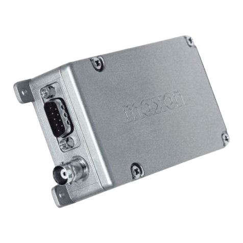
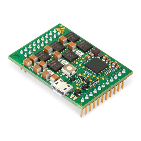
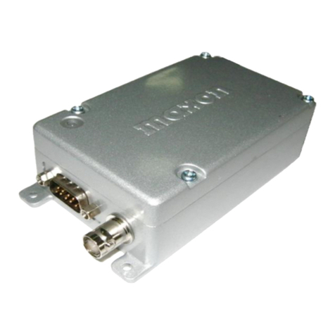
Maxon SD-125 Series User manual


MAXON
SD-125 RF LINK MODULE
i
i
TABLE OF CONTENTS…………………………………………………………………………………….…………. i
SPECIFICATIONS……………………………………………………………………………………………...………
i
UNPACKING……………………………………………………………………………………………………………. 7
INTRODUCTION………………………………………………………………………………………………………… 8
FEATURES ……………………………………………………………………………………………………………… 8
THEORY OF OPERATION ……………………………………………………………………………………………. 9
INTRODUCTION ………………………………………………………………………………………………………………… 9
DIGITAL CIRCUITS ……………………………………………………………………………………………….. 9
RF CIRCUITS ……………………………………………………………………………………………………… 9
RF CIRCUITS PLL SYNTHESIZER …………………………………………………………………………….. 10
RECEIVER …………………………………………………………………………………………………………. 10
MAINTENANCE AND REPAIR ………………………………………………………………………………………. 12
GENERAL …………………………………………………………………………………………………………. 12
REMOVING & REPLACING THE UPPER COVER ………………………………………………………….. 12
REMOVING 7 REPLACING THE DIGITAL BOARD 7 SHIELD PLATE …………………………………... 12
REMOVING 7 REPLACING THE RF BOARD ………………………………………………………………... 13
PROGRAMMING ……………………………………………………………………………………………………….. 14
ALIGNMENT PROCEDURE ………………………………………………………………………………………….. 14
RECEIVER ……………………………………………………………………………………………………….. 14
TRANSMITTER ………………………………………………………………………………………………….. 14
TEST EQUIPMENT SETUP …………………………………………………………………………………………… 17
ALIGNMENT POINTS DIAGRAM …………………………………………………………………………………………………. 18
COMPONENT REPLACEMENT ……………………………………………………………………………………………………. 19
TROBLESHOOTING GUIDE ……………………………………………………………………………………………………….. 20
VOLTAGE CHART …………………………………………………………………………………………………………………… 21
SD-125 DIGITAL BOARD (COMMON) PARTS LIST (650-010-0029) …………………………………………... 25
SD-125 (U1 400-430 MHz)RF BOARD PARTS LIST (650-020-0027) …………………………………………... 27
SD-125 (U2 440-470MHz) RF BOARD PARTS LIST (650-020-0026) ………………………………………….. 30
SD-125 (V2 148-174MHz) RF BOARD PARTS LIST (650-020-0029) ………………………………………….. 33
COMPONENT PINOUT ………………………………………………………………………………………………... 37
WRING DIAGRAM ……………………………………………………………………………………………………... 41
SCHEMATICS, BLOCK DIAGRAM & PCB´S ……………………………………………………………………… 43
BLOCK DIAGRAM ……………………………………………………………………………………………. 43
DIGITAL BOARD SCHEMATIC……………………………………………………………………………… 44
RF BOARD (148-174 MHz) SCHEMATIC …………………………………………………………………..
45
RF BOARD (400-430 MHz) SCHEMATIC ………………………………………………………………….. 46
RF BOARD (440-470MHz) SCHEMATIC ………………………………………………………………….. 47
TCOX (148-174MHz) ………………………………………………………………………………………….. 48
VCO (148 -174MHz) ………………………………………………………………………………………... 48
PAGE-i-
October 98

MAXON
SD-126 RF LINK MODULE
VCO (400-430 MHZ) ……………………………………………………………………………… 49
VCO (440-470MHz) ………………………………………………………………………………. 49
FRONT-END (148-174MHz) …………………………………………………………………….. 50
FRONT-END (400-430 MHz) ……………………………………………………………………. 50
FRONT-END (440-470MHz.) ……………………………………………………………………. 50
POWER AMPLIFIER (148-174MHz) ……………………………………………………………. 51
POWER AMPLIFIER (400-430MHz) ……………………………………………………………. 51
POWER AMPLIFIER (440-470MHz) ……………………………………………………………. 51
DIGITAL PCB ASSEMBLY……………………………………………………………………….. 52
RF PCB ASSEMBLY (148-174MHz) ……………………………………………………………. 53
RF PCB ASSEMBLY (400-430 MHz)……………………………………………………………. 54
RF PCB ASSEMBLY (440-470MHz)…………………………………………………………….. 54
EXPLODED VIEW & PARTS LIST……………………………………………………………… 55
PAGE-ii-
October 98

MAXON
SD-125 RF LINK MODULE
SPECIFICATIONS
GENERAL
Equipment Type............................................................................. Data Radio
Performance Specifications …………………………………………TIA / EIA-603 & ETS 300-113
Band………………………………………………………………………UHF / VHF
Channel Spacings………………………………………………………25 Khz, programmable
RF Output Power ……………………………………………………….5/1 watt
Modulation Type……………………………………………………….. F3D, F3E
Intermediate Frequency ……………………………………………….451 MHz & 455 MHz
Numbers of Channels…………………………………………………..16
Frequency Source……………………………………………………….SAynthesizer
Operation Rating…………………………………………………………Intermitent
90:5:5 (Standby: RXC:TX)
Power Supply…………………………………………………………….Ext.Power Supply (12 VDC Nominal Voltage)
9.0V – 15.0V DC EXTREME
TEMPERATURE RANGE
Storage……………………………………………... from-40ºC to + 80º C
Operating…………………………………………….from – 30º C to + 60ºC
Current Consumption
Standby (Muted)………………………………..< 65 mA
Transmit 5 Watts RF Power…………………..< 2.0 A
Transmit 5 Watts RF Power…………………..< 1.0 A
PAGE-1-
October 98

MAXON
Sd-125 RF LINK MODULE
Frequency Bands:
RX
TX
VHF:V1
V2
136.000 – 162.000 MHz
148.000 – 174.000 MHz
136.000 – 162.000 MHz
148.000 – 174.000 MHz
UHF:U2
440.000 – 470.000 MHz 440.000 – 470.000 MHz
U1
400.000 – 430.000 MHz 400.000 – 430.000 MHz
U5
420.000 – 450.000 MHz 420.000 – 450.000 MHz
U3
470.000 – 490.000 MHz 470.000 – 490.000 MHz
U4
490.000 – 512.000 MHz 490.000 – 512.000 MHz
Dimensions……………………………………………………..(30 mm) H x (62mm)W x (118mm)D
Weight ..................................................................................250 grams
TRANSMITTER
Nom Max Min
5W <6W >4,5 w
Carrier Power........................................
HiI ....................................................
Low ................................................. 1W <1.5W >0.8 w
Sustained Transmission …………………………Nominal conditions
5 10 30 Sec
>90% >85% >80%
Time:
Power:
Frequency Error <0,5 Khz Nominal condition for VHF
<0,75 Khz Nominal condition for UHF
-3,0 ppm Extreme condition for UHF
Frequency Deviation
25 Khz Channel Spacing ………………. Peak – 5.0, Min. – 3.8
Audio Frequency Response …………… Within + 1/-3dB of 6dB octave
@ 300 Hz to 3,0 Khz for 25 Khz C.S
Adjacent Channel Power
25 kHz …………………………………….
Conducted Spurious Emission………….
< 70 dBc @ Nominal Condition
< 65 dBc @ extreme Condition
< 57 dBc
PAGE-2-
October 98

MAXON
SD-125 RF LINK MODULE
Modulation Sensitivity ………………….. 100mmV RMS @ 60% Peak Dev.
Hum & Noise:
25 Khz Channel Spacing……………….. > 40 dB(with no PSOPH)
Modulation Symmetry…………………… < 10% Peak Dev @ 1kHz input for nominal dev + 20db
Load Stabilitty ………………………………. No osc at ≥10:1 VSWR all phase angels and suitable
antena
No destroy at ≥20:1 all phase angle
Peak Deviation Range Adjustment @ 1
kHz,Nom. Dev + 20 dB :
25 kHz Channel Spacing ………………….. Min. 3.5, Max. 6.0
RECEIVER
Sensitivity (12dB Sinad)……………………... UHF < - 117 dBm, VHF < - 118 dBm @ Nom.Condition
UHF < - 115 dBm, VHF < - 116 dBm @ Extreme
.Condition
Amplitude Characteristic……………………..
< 3dB
Adjacent Channel Selectivity ………………..
25 kHz Channel Spacing ………………. > 60 dB @ Nom., > 55dB @ Extreme Condition
Spurious Response Rejection ……………… 70 dB (100 kHz – 4 GHz)
Image Response Rejection………………… >70
IF Response ………………………………….. >70
Others ………………………………………… >70
Intermodulation Response Rejection:
± 25 kHz / 50 kHz ………………..………… 65 dB
± 50 kHz / 100 kHz ………………..………. 65 dB
Conducted Spurious Emiision @ Nominal
Conditions
9 kHz - 1 GHz ………………………….. <- 57dBm
1 Ghz – 4 GHz ………………………….. <- 47dBm
RX Spurious Emissions (Radiated) @
Nominal Conditions
9 kHz - 1 GHz ………………………….. <- 57dBm
1 Ghz – 12.75 GHz ……………………….. <- 47dBm
PAGE-3
October 98

MAXON
Sd-125 RF LINK MODULE
AF Distortion…………………………………………... < 5% @ Nom., < 10% @ Extreme Condition
25,0 kHz CP…………………………………………. < 40 dB No PSOPH
Receiver Opening Range………………………….. < 16 mS
Squelch Opening Range:…………………………… RF level for 6 to 14 dB Sinad
Squelch Closing Range (Hysteresis)……………… 0 - 6 dB Sinad@ Nominal Condition
Squelch Attack Time:
RF Level at Threshold ………………………….. < 40 mS
RF Level at Threshold + 20 dB ………………….. < 30 mS
Squelch Decay Time: ………………………………
5 mS Min, 20 mS Max
Antenna Socket Input Match………………………. > 10 dB Return Loss
L.O Frequency Temperature Stability……………. 1st - < 5ppm, 2nd < 15 ppm from – 30 to + 60 C
L.O Frequency Aging Rate ……………………….. - 2 ppm / year
REFERENCE CRYSTAL
Frequency……………………………………………….
12,8 MHz
Holder Type……………………………………………. HC – 18
Temperature Characteristics……………………….. - 5.0 ppm fom -30 C to + 60 C
-
Aging Rate …………………………………………… < 2 ppm / year in 1st year
< 1 ppm / year therafter
Lock Time……………………………………………… < 10 mS
TX to RX………………………………………………… < 20 (No Power Saving)
RX to TX ……………………………………………….. < 20
PAGE-4-
October

MAXON
SD-125 RF LINK MODULE
ENVIRONMENTAL (performance without degradation unless stated)
Temperature……………………………………………….. Deg C
Operating …………………………………………………. - 30 to + 60 C Degradation Specified @ Extreme
Storage ……………………………………………………. - 40 to + 80 C
Recharging………………………………………………….
- 10 to + 55 C
ESD…………………………………………………………. 20 Kv (C – MIC ≥15 Kv)
PROGRAMMER
Programmer ( Interface Module) ………………………. ACC-2000
Programmer ( Interface Cable) ………………………….
QPA-4000
Programmer ( Interface Software) …………………...… ACC-900
•Due to continuing research and development the company reserves the right to alter these
specifications without prior notice
PAGE – 5 –
October 98

MAXON
SD-125 RF LINK MODULE
INTRODUCTION
The Maxon SD 125 Series of RF Link Modules From
Maxon utilizes the latest technology in its design and
manufacturing. Both he UHF and VHF models (Phase
Lock Loop Synthesizer) / microprocessor controlled,
And offer one to five watts of power with 16 channel
capability . Multiple functions including 1200 to 9600
baud rates, AC and/or DC audio coupling, GMSK and
FSK modulation are standard in these fully
programmable wide bandwidth RF Link Module units.
The radio is programmed using a IBM Personal
Computer, DOS based software, an interface module
and a programming cable. This allows the radio to be
tailored to meet the requirements of the individual user
and of the System (s) it is operating within.
FEATURES
•Busy Channel Lockout
•16 Channels
•TX Time-out
•Power Save
•1/5 Watt Programmable Output
•15 kHz Programmable Spacing
Busy Channel Lockout
The Busy Channel Lockout feature , when
enabled, disables the transmitter when the
receiving channel is busy and the user
attempts to transmit.
16 Channels
The SD-125 Series radio can store up to
16channels within the same band
TX Time – Out
The TX Time-Out feature, when enabled,
limits the amount of time that the user can
continuously transmit. This time can be set in
increments of 10 seconds from 10 seconds to
990 seconds
Power Save
The Power Save feature is used when an
external battery is used as the power source.
When Power Save is enable, the receiver ON
and OFF time can be programmed into the
radio and allows the operator to set the length
of time the receiver is asleep.
PAGE-6-
October 98

INTRODUCTION
The VHF and UHF radios are comprised of two PCB's (an
RF PC Band a digital PCB). These boards are connected
with an 18 pin female and male connector. The digital board
is interfaced with external data equipment through the 9 pin
d-sub male connector, which controls the radio and data
receiving and sending.
DIGITAL CIRCUITS
The Digital circuit contains the CPU, the channel select
switch, and associated digital circuits.
TX-SIGNAL CIRCUIT
The TX data signal comes from Pin 2 of Con 401, and goes
through U404D. The TX-signal is amplified by U406C. The
TX-signal is filtered by U405A & B which is a 4’Th order low
pass filter, the output of U405A is then fed to the RF board
for TX modulation.
RX-SIGNAL CIRCUIT
The RX- data signal comes from the RF board, which is
connected with pin 10 of Con 403. The RX-signal is switched
by U404A and adjusted by RV403 and amplified by U407.
The amplified signal goes to pin10 of Con 401.
RSSI DETECTOR
From the RF board, the RSSI (Received Signal Strength
Indicator) signal flows to U403A&Bthrough R461. The pulse
is injected from pin 5 of U403B every 1 mS and C451 is
discharged. It is then charged by R464. The RSSI signal is
simultaneously input to pin 7 of U403A and those signals are
compared. The compared signal is output from U403A. Pin 1
of U403A and the CPU detects the pulse width. The pulse
width is varied by RSSI DC voltage; therefore, the carrier
detection is controlled by the CPU.
EEPROM
RX / TX channel and RSSI detection level as well as other
data from the programmer are stored in the EEPROM. The
data stored is retained without power supplied. This is a non-
volatile memory. The EEPROM may have information re-
programmed or erased. U402 is an EEPROM with 2048 (8 x
256) capacity and data is written and read serially.
MAXON
SD-125 RF LINK MODULE
CHANNEL SELECTOR
One of 16 channels may be selected using the Dip Switch
(SW401). SW401 encodes the channel number, selected
into 4-bit binary code. The binary code plus one equals the
channel number. The binary code is decoded by the CPU
enabling the appropriate RX or TX frequency and
associated data to be selected from the EEPROM.
DC TO DC CONVERTER
The main DC power is injected to the DC to DC converter.
The DC to DC converter regulates the various input power
supply voltage and outputs a constant voltage of 7.5 Volts.
It is a source for all of the RF and digital circuits.
The DC to DC converter is formed by U801, Q801, Q802,
L801 and R804. U801 is a switch mode DC to DC
Converter IC.
Input DC various appears as a voltage various through
R804.
U801 detects the voltage and controls the switching pulse.
As the switching pulses, Q801and Q802 switches the input
DC of various supply voltages and generates the constant
DC of supply voltage.
RF CIRCUITS
TRANSMITTER
The transmitter is comprised of:
1. Buffer
2. P.A. Module
3. Low Pass Filter
4. Antenna Switch
5. A.P.C. Circuits
BUFFER
VCO output level is -6dBm and amplified to +10dBm
(UHF), +6dBm (VHF). The buffer consists of Q16 and Q17
for isolation and gain.
P.A. MODULE
The P.A. Module contains Q501, Q502, and Q503. Three
stage amplifiers Q501 amplify the TX signal from +10 dBm
to 100 mW. Q502 is amplified to 0.5W. Q503 amplifies to
3W and then matched to 50 Ohms using the L.C. network,
thereby reducing the harmonics by -30 dB.
LOW PASS FILTER
L7, L8, L11, C72, C73, C74 and C75 are the 7th order
Chebyshev low pass filter. Unwanted harmonics are
reduced by -70 dBc.
PAGE-7-
October 98
MAXON
SD-125 RF LINK MODULE
ANTENNA SWITCH
When transmitting, the diodes D5 and D6 are forward biased
enabling the RF signal passage to the antenna. D6 is
shorted to ground inhibiting the RF signal to front end. In
receive the diodes D5 and D6 are reversed biased passing
the signal from the antenna through L13 and C83 to the front
end without signal loss.
AUTOMATIC CURRENT CONTROL (ACC)
CIRCUITS
The ACC circuit consists of R109, variable resistor RV1,
IC3(B) and transistors Q21 and Q22. The supply current is
monitored by the difference voltage on R109 (0.1 Ohm). If
the current varies by RF power output or other reasons, it
produces some bias voltage by IC3A and Q19. The
differential signal at the output of IC3 is passed to Q21 and
Q22 that produces a constant power output to the antenna.
RV1 is used to adjust the RF power level.
RF CIRCUITS PLL SYNTHESIZER
12.8 MHz TCXO
The TCXO contains the 3-stage thermistor network
compensation and crystal oscillator and modulation ports.
Compensation is ±5 PPM or less from -30c to +60c.
PLL IC DUAL MODULES PRESCALER
Input frequency of 12.8 MHz to IC2 MC14519 pin 20 is
divided to 6.25 kHz or 5 kHz by the reference counter, and
then supplied to the comparator. RF signal input from VCO is
divided to 1/64 at the prescaler in IC2, divided by A and N
counter in IC2 to determine frequency steps, and then
supplied to the comparator. PLL comparison frequency is
6.25/5kHz so that minimum programmable frequency step is
5/6.25 kHz.
The A and N counter is programmed to obtain the desired
frequency by serial data in the CPU. In the comparator, the
phase difference between reference and VCO signal is
compared. When the phase of the reference frequency is
leading , Fv is the output, but when VCO frequency is
leading, Fr is the output. When Fv = Fr, phase detector out is
a very small pulse. 64/65 modulus prescaler is comprised in
IC2, and has two output ports:
•Port A pin 16: TX enable 2
•Port B pin 15: prescaler power save control in PLL
IC Pin 13 labeled test2 allows the technician to see
the output of the dual modulus prescaler for trouble
shooting purposes, no connection should be made
to this pin.
LEVEL SHIFTER & CHARGE PUMP
The charge pump is used for changing output signals Fr,
Fv at PLL IC from 0-5v to 0-12v necessary for controlling
the VCO.
REFERENCE FREQUENCY LPF
The Loop Filter contains R12, C21 and C22. LPF settling
time is 12mS with 1 kHz frequency. This also reduces the
residual side-band noise for the best signal-to-noise ratio.
DC TO DC CONVERTER
The DC to DC converter convert the 5v to 14-16v to supply
the necessary voltage for wide range frequency in the
VCO.
VCO
The VCO consist of an RX VCO and a TX VCO. It is
switched TX/RX by the power source. It is configured as a
colpits oscillator and connected to the buffer as a cascade
bias in order to save power. The varicap diode D201/D301
are low-resistance elements and produce a change in
frequency with a change in reverse bias voltage (2-11v).
L203/L303 are resonant coils, which changes the control
voltage by the tuning core. D202 modulation diode,
modulates the audio signal.
C204 compensates for the non-linearity of the VCO due to
modulation diode, and maintains a constant modulation
regardless of frequency.
RECEIVER
FRONT-END
The receive signal is routed backward through the low
pass filter, then onward to Pin 1 of the Hybrid Receiver
Front End Module to a bandpass filter consisting of (VHF
C622 through C608, L607 through L604 ) and (UHF
C601through C610, L601 through L603 ) is coupled to the
base of Q601 which serves as an RF amplifier. Diode
D601 serves as protection from static RF overload from
nearby transmitters. The output of Q601 is then coupled to
a second bandpass filter consisting of (VHF C607 through
C623 and L604 through L607).The output of Pin 6 is then
coupled to the doubly balanced mixer D9. The receiver
front end module is factory pre-tuned and requires no
adjustment. Repair is effected by replacement of the entire
module of the proper banded module. These are VHF
148MHz to 174 MHz and UHF 440 MHz to 470 MHz. The
receiver front end module signal pins are as follows:
1. RF Input
2. Input Ground
3. N/A
4. Receive +5V
5. Ground
6. Output
PAGE- 8-
October 98

FIRST MIXER
D9, T2 and T3 are double balanced mixers which provide the
45.1 MHz intermediate frequency output. The filtered
frequency from the front end module is coupled to T2 . The
45.1 MHz IF output is matched to the input of the 2-pole
monolithic filter by L14, L31, C69 and C97. The crystal filter
provides a bandwidth of ±7.2 kHz from the operating
frequency providing a high degree of spurious and
intermodulation protection.
Additionally, a 90 MHz trap (XF1) is also placed at the filter
output to provide additional attenuation of the second order
IMD. The output of the filter is impedance matched by C97
and C69 to the base of the post of filter IF amplifier Q25.
SECOND OSCILLATOR MIXER LIMITER AND
FM DETECTOR
The output of the post filter amplifier, Q25, is coupled via
C98 to the input of IC5 ( MC3371). IC5 is a monolithic single
conversion FM transceiver, containing a mixer, the second
local oscillator, limiter and quadrature detector. Crystal X1
44.645 MHz is used to provide resultant 455kHz signal from
the output of the second mixer. The mixer output is then
routed to CF1 (455F). These ceramic filters provide the
adjacent channel selectivity of 25 kHz bandwidth .
RSSI ( RECEIVER SIGNAL STRENGTH
INDICATOR )
The RSSI signal is output from IC5 on pin 13. As the receiver
signals the output, DC voltage is varied as much as receiver
signal strength. Also, the DC signal is temperature
compensated with a thermistor (TH1).
MAXON
SD-125 RF LINK MODULE
PAGE- 9-
October 98

MAXON
SD-125 RF LINK MODULE
GENERAL
When removing or fitting, use the Exploded View and Parts
List, located on page 55 in conjunction with the following
procedures:
•WARNING: Disconnect the SD-125 from all
external equipment at the D-Sub connector prior to
disassembly.
REMOVING & REPLACING THE UPPER
COVER
Removing the Upper Cover:
1. Unscrew the four upper cover mounting screws
located on the upper cover of the radio.
To replace the Upper Cover:
1. Reverse the steps taken to remove the Upper
Cover.
REMOVING & REPLACING THE DIGITAL
BOARD & SHIELD PLATE
Removing the Digital Board Assembly & Shield
Plate:
1. Remove the Upper Cover (refer to Removing &
Replacing the Upper Cover).
2. Disconnect the DB9 pin connector on CON401.
3. Unscrew the 4 mounting screws.
4. Remove the Digital Board Assembly.
5. Remove the Shield Plate.
To replace the Digital Board Assembly:
1. Reverse the steps taken to remove the Digital
Board Assembly & Shield Plate.
PAGE-10-
October 98

REMOVING & REPLACING THE RF
BOARD
Removing the RF Board Assembly:
1. Remove the Upper Cover (refer to Removing &
Replacing the Upper Cover).
2. Remove the Digital Board Assembly and Shield
Plate (refer to Removing & Replacing the Digital
Board Assembly & Shield Plate).
3. Unscrew the 4 mounting standoffs.
4. Unsolder the antenna connector cable.
5. Remove the RF Board Assembly.
To replace the RF Board Assembly:
1. Reverse the steps taken to remove the RF Board
Assembly.
MAXON
SD-125 RF LINK MODULE
Figure 4-RF Board Removal
PAGE-11-
October 98

MAXON
SD-125 RF LINK MODULE
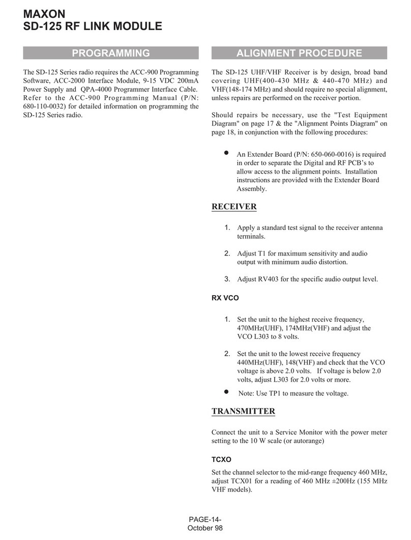
The SD-125 Series radio requires the ACC-900
Programming Software, ACC-2000 Interface Module,
9-15 VDC 200mA Power Supply and QPA-4000
Programmer Interface Cable.
Refer to the ACC-900 Programming Manual (P/N: 680-
110-0032) for detailed information on programming the
SD-125 Series radio.
The SD-125 UHF/VHF Receiver is by design, broad
band covering UHF(400-430 MHz & 440-470 MHz)
and VHF(148-174 MHz) and should require no
special alignment, unless repairs are performed on
the receiver portion.
Should repairs be necessary, use the "Test
Equipment Diagram" on page 17 & the "Alignment
Points Diagram" on page 18, in conjunction with the
following procedures:
• An Extender Board (P/N: 650-060-0016) is
required in order to separate the Digital and
RF PCB.s to allow access to the alignment
points. Installation instructions are provided
with the Extender Board Assembly.
RECEIVER
1. Apply a standard test signal to the receiver
antenna terminals.
2. Adjust T1 for maximum sensitivity and audio
output with minimum audio distortion.
3. Adjust RV403 for the specific audio output
level.
RX VCO
1. Set the unit to the highest receive frequency,
470MHz(UHF), 174MHz(VHF) and adjust
the VCO L303 to 8 volts.
2. Set the unit to the lowest receive frequency
440MHz(UHF), 148(VHF) and check that the
VCO voltage is above 2.0 volts. If voltage is
below 2.0 volts, adjust L303 for 2.0 volts or
more.
• Note: Use TP1 to measure the voltage.
TRANSMITTER
Connect the unit to a Service Monitor with the power
meter setting to the 10 W scale (or autorange)
TCXO
Set the channel selector to the mid-range frequency
460 MHz, adjust TCX01 for a reading of 460 MHz
±200Hz (155 MHz VHF models).
PAGE-12-
October 98

TX VCO
1. Set the unit to the highest transmit frequency,
470MHz(UHF), 174MHz(VHF) key the
transmitter and adjust the VCO L203 to 8
volts.
2. Set the unit to the lowest transmit frequency
440 MHz(UHF), 148(VHF) key the transmitter
and check that the VCO voltage is above 2.0
volts. If voltage is below 2.0 volts, adjust L203
for 2.0 volts or more.
Note: use TP1 to measure the voltage.
TX Deviation and Balance Adjustment
1. Set the unit to a mid-frequency and input the
TX data with 400 Hz standard audio level.
2. Increase the signal level to 20 dB from
standard level.
3. Monitor the demodulated signal from service
monitor. Adjust RV3 to make the monitored
signal to be a balanced square wave.
4. Reduce input signal to the standard level and
adjust RV2 for the standard deviation.
APC
1. Adjust RV1 for High Power (5W)
2. Adjust RV6 for Low Power (1W)
3. This completes the transmitter alignment
procedures.
SD-125 Squelch setting using the ACC-2000
Interface Module
Maxon.s wide range of data radio products since the
crystal control module (DM-0500 series) had their
squelch level setting by hardware touch up. With the
new SD-125 series, the squelch level to open or close
(unmute or mute) is set up by software control.
The RSSI utilizes the A/D conversion that will be fed to
the microprocessor, which in turn will use this input to
determine the squelch level setting to control the mute
and unmute of the receiver.
Default setting of squelch level for all the SD-125 from
our manufacture and workshop is approximately set at:
MAXON
SD-125 RF LINK MODULE
1. Squelch open (unmute) at -114dBm to -
113dBm (0.45 - 0.5mV of the RX signal
strength)
2. Squelch close (mute) at -117dBm to -
116dBm (0.3 - 0.35mV of the RX signal
strength)
Changing the default squelch settings requires use
of the programming adaptor box. This box is
designed for use not only as part of the
programming kit but also as a tool of squelch level
setting.
The minimum equipment required for squelch level
setting is a RF signal generator. Radio
communication test equipment is recommended.
1. Power up the programming adaptor box (use the
DC supply of 9 - 15 Volts 200mA).
2. Hook up the SD-125 unit to the programming
adaptor box, and its antenna connector to the RF
input port of the RF signal generator.
3. With the adaptor box turned "off., simultaneously
press and hold both "ON/OFF" and "WRITE" buttons
down.
4. Release the "ON/OFF" button first then the
"WRITE" button next. (LED indicator on the box will
flash twice after that it may stay on / off, this is of no
concern , because depending on the signal strength
of the RF generator as well as the pre-set level of
squelch the SD125 may be in standby mode (LED
OFF) or in receiving mode (LED ON)
5. Adjust the RF signal generator for the desired
signal strength to OPEN squelch (e.g. default setting
is -113dBm, that is equivalent to 0.5mV)
6. Press and release "READ" button, LED indicator
will flash 3 times then it will be ON.
7. Adjust the RF signal generator for the desired
signal strength to CLOSE squelch (e.g. default
setting is -116dBm, that is equivalent to 0.35mV)
8. Press and release "READ" button, LED indicator
will flash 1 time then it will be OFF.
9. Press and release "WRITE" button, LED indicator
will flash twice.
10. Squelch level is now set. Test for desired level
by increasing or decreasing the RF signal to levels
set
PAGE-13-
October 98

MAXON
SD-125 RF LINK MODULE
for open and close squelch (mute LED will be OFF &
unmute LED will be ON).
NOTE: The difference of RF signal strength
between the unmute and mute levels must be
greater than or at least equal to 0.15mV (i.e. at
least -123.5dBm) for the squelch setting to
work properly. If they are too close to one
another, RSSI through the A/D conversion can
not differentiate between the mute and unmute
level properly. As a result, it would cause the
CD (Carrier Detect) to act intermittently.
PAGE-14-
October 98

MAXON
SD-125 RF LINK MODULE
PAGE-15-
October 98

MAXON
SD-125 RF LINK MODULE
PAGE-16-
October 98

COMPONENT REPLACEMENT
Surface Mount Components
Surface mount components should always be replaced using
a temperature controlled soldering system. The soldering
tools may be either a temperature controlled soldering iron or
a temperature controlled hot-air soldering station. A hot-air
system is recommended for the removal of components on
these boards. With either soldering system, a temperature
of 700 F (371 C) should be maintained.
The following procedures outline the removal and
replacement of surface mount components. If a hot-air
soldering system is employed, see the manufacturer s
operating instructions for detailed information on the use of
your system.
CAUTION: Avoid applying heat to the body of any
surface mount component using standard soldering
methods. Heat should be applied only to the
metalized terminals of the components. Hot-air
systems do not damage the components since the
heat is quickly and evenly distributed to the external
surface of the component
CAUTION: The CMOS Integrated Circuit devices
used in this equipment can be destroyed by static
discharges. Before handling one of these devices,
service technicians should discharge themselves by
touching the case of a bench test instrument that
has a 3-prong power cord connected to an outlet
with a known good earth ground. When soldering
or desoldering a CMOS device, the soldering
equipment should have a known good earth
ground.
Surface Mount Removal
1 . Grip the component with tweezers or small needle
nose pliers.
2. Alternately heat the metalized terminal ends of
the surface mount component with the soldering
iron. If a bot-air system is used, direct the heat to
the terminals of the component Use extreme care
with the soldering equipment to prevent damage
to the printed circuit board (PCB) and the
surrounding components.
3. When the solder on all terminals is liquefied,
gently remove the component Excessive force
may cause the PCB pads to separate from the
board if all solder is not completely liquefied.
4. lt may be necessary to remove excess solder
using a vacuum de-soldering tool or Solder wick.
Again, use great care when de-soldering or
soldering on the printed circuit boards. It may also
be necessary to remove the epoxy adhesive that
was under the
MAXON
SD-125 RF LINK MODULE
surface mount component and any flux on the printed
circuit board.
Surface Mount Component Replacement
1. Tin one terminal end of the new component and
the corresponding pad of the PCB. Use as little
solder as possible.
2. Place the component on the PCB pads,
observing proper polarity for capacitors, diodes,
transistors, etc.
3. Simultaneously touch the tinned terminal end
and the tinned pad with the soldering iron.
Slightly press the component down on the
board as the solder liquefies. Solder all
terminals, allowing the component time to cool
between each application of heat. Do not apply
heat for an excessive length of time and do not
use excessive solder.
With a hot-air system, apply hot air until all tinned areas
are melted and the component is seated in place. lt may
be necessary to slightly press the component down on the
board. Touch up the soldered connections with a standard
soldering iron if needed. Do not use excessive solder.
•CAUTION: Some chemicals may damage the
internal and external plastic parts of the radio.
4. Allow the component and the board to cool and
then remove all flux from the area using alcohol
or another approved flux remover.
Surface Mounted Integrated Circuit
Replacement
Soldering and de-soldering techniques of the surface
mounted IC s are similar to the above outlined procedures
for the surface mounted chip components. Use extreme
care and observe static precautions when removing or
replacing the defective (or suspect) IC s. This will prevent
any damage to the printed circuit board or the surrounding
circuitry.
The hot-air soldering system is the best method of
replacing surface mount IC s. The IC s can easily be
removed and installed using the bot-air system. See the
manufacturer s instructions for complete details on tip
selection and other operating instructions unique to your
system. If a hot-air system is not available, the service
technician may wish to clip the pins near the body of the
defective IC and remove it. The pins can then be removed
from the PCB with a standard soldering iron and tweezers,
and the new IC installed following the Surface Mount
Component Replacement procedures. it may not be
necessary to tin all (or any) of the IC pins before the
installation process.
PAGE - 17
October 98
COMPONENT REPLACEMENT
Other manuals for SD-125 Series
3
This manual suits for next models
2
Table of contents
Other Maxon Control Unit manuals

Maxon
Maxon ESCON 50/8 Application guide

Maxon
Maxon SD-125 Series User manual

Maxon
Maxon ESCON 50/5 Application guide

Maxon
Maxon ESCON 24/2 Application guide

Maxon
Maxon SD-125 Series User manual

Maxon
Maxon ESCON 50/4 EC-S Application guide

Maxon
Maxon SD-125 Series User manual

Maxon
Maxon SD-17OEX Series Operator's manual