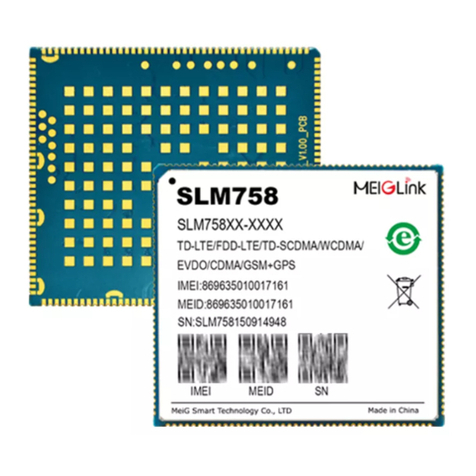
MEIG SRM825N-NA User manual

MeiG SRM825N-NA Module Hardware Design Manual
MeiG Smart Technology Co., Ltd.
1/13
MeiG SRM825N-NA Module
User Manual

MeiG SRM825N-NA Module Hardware Design Manual
MeiG Smart Technology Co., Ltd.
1/13
Important Notice
Copyright Notice
All rights reserved. MeiG Smart Technology Co., Ltd
This manual and all its contents are owned by MeiG Smart Technology Co., Ltd and
protected by Chinese laws and relevant copyright laws in applicable international
conventions. Without the written authorization of MeiG Smart Technology Co., Ltd, no one
may copy, disseminate, distribute, modify or use part or all of this manual in any form, and
the offenders will be held responsible according to law.
Statement of No Guarantee
MeiG Smart Technology Co., Ltd makes no representations or guarantees, either express or
implied, for any contents in this document, and assumes no responsibility for the
merchantability and fitness for a particular purpose or any indirect, extraordinary or
consequential losses.
Disclaimer
The company assumes no responsibility for property damage or personal injury caused by
customers’ improper operation. Customers are requested to develop corresponding
products according to the technical specifications and reference designs in the manual.
Before the disclaimer, the company has the right to change the contents of this manual
according to the needs of technological development, and the version is subject to change
without further notice.

MeiG SRM825N-NA Module Hardware Design Manual
MeiG Smart Technology Co., Ltd.
2/13
1 Introduction
This document defines SRM825N module air interface and hardware interface for connecting the
module to applications of customers.
This document can help customers quickly understand the interface specifications, electrical
characteristics, mechanical specifications and related product information of SRM825N module. With the
help of this document, according to our application manual and user guide, customers can quickly apply
SRM825N module to wireless applications.
1.1 Safety Instructions
By complying with the following safety principles, you can ensure personal safety and protect the
products and working environment from potential damage:
Driving safety first! When you drive, do not use handheld mobile terminal device
unless it has a hands-free function. Please stop the car before calling!
Please turn off the mobile terminal device before boarding. The wireless function
of mobile terminal shall not be turned on in the aircraft to prevent interference with
the aircraft communication system. Ignoring this reminder may affect flying safety
or even violate the law.
In hospitals or health care facilities, pay attention to whether there are restrictions
on the use of mobile terminal device. RF interference will cause medical
equipment to be abnormal, so mobile terminal device may need to be turned off.
Mobile terminal device cannot always be effectively connected, for example, if the
mobile device has no expense or the SIM is invalid. When you encounter the
above situations in an emergency, please make an emergency call, meanwhile,
ensure that your device is turned on and in an area with sufficient signal strength.
Your mobile terminal device will receive and transmit radio frequency signals
when it is turned on. There will be radio frequency interference when it is close to
TV, radio, computer or other electronic equipment.

MeiG SRM825N-NA Module Hardware Design Manual
MeiG Smart Technology Co., Ltd.
3/13
Please keep mobile device away from inflammable gases. Please turn off the
mobile terminal device when you are near a fueling station, oil depot, chemical
plant or explosion site. There will be potential safety hazards when operating
electronic equipment in any place with potential explosion hazard.
1.2 Purpose of the Document
This document mainly describes the hardware interface and structural characteristics of the SRM825N
wireless module, and guides users to embed the SRM825N module in the design of various application
terminals.
1.3 FCC Statement
Federal Communication Commission Interference Statement
This device complies with part 15 of the FCC Rules. Operation is subject to the following two conditions:
(1) This device may not cause harmful interference, and (2) this device must accept any interference
received, including interference that may cause undesired operation。
This equipment has been tested and found to comply with the limits for a Class B digital device, pursuant
to part 15 of the FCC Rules. These limits are designed to provide reasonable protection against harmful
interference in a residential installation. This equipment generates, uses and can radiate radio frequency
energy and, if not installed and used in accordance with the instructions, may cause harmful interference
to radio communications. However, there is no guarantee that interference will not occur in a particular
installation. If this equipment does cause harmful interference to radio or television reception, which can
be determined by turning the equipment off and on, the user is encouraged to try to correct the
interference by one or more of the following measures:
- Reorient or relocate the receiving antenna.
- Increase the separation between the equipment and receiver.
- Connect the equipment into an outlet on a circuit different from that to which the receiver is connected.
- Consult the dealer or an experienced radio/TV technician for help.
Changes or modifications not expressly approved by the party responsible for compliance could void the
user‘s authority to operate the equipment。
Radiation Exposure Statement
This equipment complies with FCC radiation exposure limits set forth for an uncontrolled environment.
This equipment should be installed and operated with minimum distance 20 cm between the radiator &
your body.
1.4 Important Notice to OEM integrators
1. This module is limited to OEM installation ONLY.

MeiG SRM825N-NA Module Hardware Design Manual
MeiG Smart Technology Co., Ltd.
4/13
2. This module is limited to installation in fixed applications, according to Part 2.1091(b).
3. The separate approval is required for all other operating configurations, including portable
configurations with respect to Part 2.1093 and different antenna configurations.
4. For FCC Part 15.31 (h) and (k): The host manufacturer is responsible for additional testing to verify
compliance as a composite system. When testing the host device for compliance with Part15 Subpart B,
the host manufacturer is required to show compliance with Part 15 Subpart B while the transmitter
module(s) are installed and operating. The modules should be transmitting and the evaluation should
confirm that the module's intentional emissions are compliant (i.e. fundamental and out of band
emissions). The host manufacturer must verify that there are no additional unintentional emissions other
than what is permitted in Part 15 Subpart B or emissions are complaint with the transmitter(s) rule(s).The
Grantee will provide guidance to the host manufacturer for Part 15 B requirements if needed.
Note:
notice that any deviation(s) from the defined parameters of the antenna trace, as described by the
instructions, require that the host product manufacturer must notify to MeiG Smart Technology Co., Ltd.
that they wish to change the antenna trace design. In this case, a Class II permissive change application
is required to be filed by the USI, or the host manufacturer can take responsibility through the change in
FCC ID (new application) procedure followed by a Class II permissive change application
End Product Labeling
When the module is installed in the host device, the FCC/IC ID label must be visible through a window
on the final device or it must be visible when an access panel, door or cover is easily re-moved. If not, a
second label must be placed on the outside of the final device that contains the following text: “Contains
FCC ID: 2APJ4-SRM825NNA”,The FCC ID can be used only when all FCC mpliance requirements are
met.
Manual Information to the End User
The OEM integrator has to be aware not to provide information to the end user regarding how to install or
remove this RF module in the user’s manual of the end product which integrates this module. The end
user manual shall include all required regulatory information/warning as show in this manual
This device is intended only for OEM integrators under the following conditions: (For module device use)
1) The antenna must be installed such that 20 cm is maintained between the antenna and users, and 2)
The transmitter module may not be co-located with any other transmitter or antenna. As long as 2
conditions above are met, further transmitter test will not be required. However, the OEM integrator is
still responsible for testing their end-product for any additional compliance requirements required with
this module installed.
2 Product Overview
2.1 Basic Description

MeiG SRM825N-NA Module Hardware Design Manual
MeiG Smart Technology Co., Ltd.
5/13
The MeiG Smart SRM825N module is a 5G NR Sub-6GHz module specially designed for IoT and eMBB
applications. It integrates Qualcomm’s latest generation of Snapdragon SDX62 baseband chip.
Complies with 3GPP Release 16 standards and can support independent two types of network
deployments: SA and NSA. For different target regions, different sub-models are designed to support a
variety of 3G/4G/5G network standards, which can cover the 5G commercial network frequency bands
of major regions and operators around the world.
At the same time, the SRM825N module supports Qualcomm I Z a t ™ Gen 9 positioning technology, a
built-in multi-constellation high-precision GNSS receiver, can support GPS/GLONASS/BeiDou/Galileo/
QZSS, and can provide fast and accurate positioning services.
SRM825N supports a wealth of industry standard interfaces to facilitate peripheral expansion, supports
USB3.1, PCIe3.0, GPIO, PCM and other interfaces, compatible with multiple types of operating systems
(Android, Linux, Windows 7/8/10 and other operating systems) ), built-in rich network protocols, with
interface standards, simple baseboard design, easier assembly and other advantages, can be widely
used in CPE home gateways, high-definition TV, AR/VR, industrial routers, set-top boxes, vehicle
terminals, video surveillance, industrial Internet and other fields.
2.2 Product Overview
The following table lists the frequency bands supported by SRM825N-NA sub-model:
Table 1 Frequency Bands Supported by SRM825N Module
Product
Description
SRM825N-NA
⚫5G NR NSA:
N2/N5/N7/N12/N13/N14/N25/N38/N41/N48/N66/N71/N77/N78
⚫5G NR SA:
N2/N5/N7/N12/N13/N14/N25/N38/N41/N48/N66/N71/N77/N78
⚫LTE FDD: B2/B4/B5/B7/B12/B13/B14/B17/B25/B26/B66/B71
⚫LTE TDD: B38/B41/B42/B43/B48
⚫WCDMA: B2/B4/B5
⚫Support digital voice (optional)
Table 2 Main Features of the Module
Parameter
Description
Power supply
⚫VIN supply voltage range: 3.135V ~ 4.4V (3.135V only guarantees
the module function, but does not guarantee the RF performance. The
lowest voltage to meet the RF performance requires 3.3V)
⚫Typical supply voltage: 3.8V
Transmitting power
⚫Class 2 (26dBm+2/-3dB) for 5G NR;
SRM825N-NA: N41/N77/N78;
⚫Class 2 (26dBm+2/-3dB) for 4G;
SRM825N-NA: B41
⚫Class 3 (23dBm±2.7dB) for LTE bands and 5G NR;

MeiG SRM825N-NA Module Hardware Design Manual
MeiG Smart Technology Co., Ltd.
6/13
SRM825N-NA:
LTE FDD: B2/B4/B5/B7/B12/B13/B14/B17/B25/B26/B66/B71
LTE TDD: B38/B42/B43/B48
5G NR : N2/N5/N7/N12/N13/N14/N25/N38/N48/N66/N71
⚫Class 3 (24dBm+1.7/-3.7dB) for WCDMA bands;
SRM825N-NA:B2/B4/B5
LTE features
⚫Supports a maximum of 5CA CAT19
⚫Support 1.4 ~ 20 MHZ radio frequency bandwidth
⚫Supports DL 4X4 MIMO:
SRM825N-NA: B2/B4/B7/B25/B66/B38/B41/B42/B43/B48
⚫Supports the following modulation types:
Uplink: QPSK, 16QAM, 64QAM and 256QAM
Downlink: QPSK, 16QAM, 64QAM, and 256QAM
⚫The maximum uplink rate is 200Mbps, and the maximum downlink
rate is 1.6 Gbps
WCDMA features
⚫Support 3GPP DC-HSPA+
⚫Support 16-QAM, 64-QAM and QPSK modulation
⚫3GPP R6 CAT6 HSUPA: Max uplink rate 5.76Mbps
⚫3GPP R8 CAT24 DC-HSPA+: Max downlink rate 42Mbps
5G NR features
⚫Supports the 3GPP R16 standard, supporting SA/NSA
⚫Supports the following modulation types:
Uplink: π/2-BPSK, QPSK, 16QAM, 64QAM, and 256QAM
Downlink: QPSK, 16QAM, 64QAM and 256QAM
⚫Support MIMO:
U UL 2x2 MIMO:
SRM825N-NA: N41/N48/N77/N78
DL 4x4 MIMO:
SRM825N-NA: N2/N7/N25/N38/N48/N66/N77/N78
⚫SUB 6G Supports SCS 15 kHz (FDD) and 30 kHz (TDD)
⚫Supports SRS:
SA 2T4R:
SRM825N_NA:N41/N77/N78
NSA 1T4R:
SRM825N_NA:N41/N77/N78
⚫The Sub6 SA mode provides a maximum uplink rate of 900 Mbit/s
and a maximum downlink rate of 2.4 Gbps
Network protocol features
⚫Support TCP/UDP/PPP/PING/NITZ/QMI protocol
⚫Support PAP (Password Authentication Protocol) and CHAP
(Challenge Handshake Authentication Protocol)
Short Message Service
(SMS)
⚫Text and PDU modes
⚫Point-to-point MO and MT
⚫Short message storage: stored in the module by default
USIM card interface
⚫Support USIM/SIM card: 1.8V and 3V, USIM2 compatible with
eSIM (2*2)
Audio features
⚫Support 1 digital audio interface: PCM interface
⚫WCDMA: AMR/AMR-WB
⚫LTE: AMR/AMR-WB
⚫5G NR: AMR/AMR-WB
PCM interface
⚫For audio use, external codec chip is required
⚫Support 8-bit A-law, u-law and 16-bit linear coding formats

MeiG SRM825N-NA Module Hardware Design Manual
MeiG Smart Technology Co., Ltd.
7/13
⚫Support long frame mode and short frame mode
⚫Support master and slave modes, but it can only be used as
master mode in long frames
USB interface
⚫Compatible with USB3.1 gen2 feature (only supporting slave
mode), max. data transmission rate 10.0Gbps
⚫Used for AT command, data transmission, GNSS NMEA output,
software debugging and upgrade USB driver: support Windows7,
Windows 8/8.1, Windows10, Linux 2.6 or higher versions,
Android2.3/4.0/4.2/4.4/5.0/5.1/6.0/7.0/8.0/9.0/10.0
GNSS features
⚫Qualcomm Gen9C-Lite
⚫Protocol: NMEA 0183
RX-diversity
⚫Support 5G NR/LTE/WCDMA diversity
AT command
⚫Compliant with 3GPP TS 27.007, 27.005, newly add MeiG AT
command
Network indication
⚫WWAN_LED# pin indicates the status of the RF network
Antenna interface
⚫ANT0, ANT1, ANT2, ANT3
⚫GNSS antenna interface ANT_GNSS
Physical properties
⚫Size: 30.0*52.0*2.3mm
⚫Weight: <8g
Temperature range
⚫Normal working temperature: -30℃ ~ +75℃
⚫Extended working temperature: -40℃ ~ +85℃
⚫Storage temperature: -45℃ ~ +90℃
Software upgrade
⚫USB interface upgrade, FOTA upgrade
RoHS
⚫All parts are fully compliant with EU RoHS standard
3.3 Power Supply
3.3.1 Pin Description
The description in this section is related to the power supply. The interfaces involved include the
following:
Table 3 Power related interface
Pin
name
Pin number
Description
Min.
Value
Typical
Value
Max.
Value
Unit
VIN
2,4,70,72,74
PI
3.135
3.8
4.4
V
GND
3,5,11,27,33,39,45,51,57,71,
73
Ground
-
0
-
V
3.11 Antenna Interface

MeiG SRM825N-NA Module Hardware Design Manual
MeiG Smart Technology Co., Ltd.
8/13
3.11.1 Antenna Definition
SRM825N module provides 5 antenna pins, which are: GNSS, ANT0, ANT1, ANT2, ANT3, as shown in
the table below.
Table 4 Antenna Pin Assignment
ANT_port
ANT_GNSS
ANT0(TRX)
ANT1(TRX)
ANT2(TRX)
ANT3(RX)
Band
GNSS L1
LB DRX
MHB TRX0
N41 TRX0
N48/N77/78
PRX1
MHB PRX1
N41 PRX1
N48/N77/78
TRX0
LB TRX
MHB DRX
N41 TRX1
N48/N77/78
DRX1
MHB DRX1
N41 DRX1
N48/N77/78
DRX0/TRX1
Frequency
1559-1610MHz
600-2690MHz
3300-5000MHz
1452-2690MHz
3300-5000MHz
600-2690MHz
3300-5000MHz
1452-2690MHz
3300-5000MHz
Notes:
1. RF informations:
MHB:
FDD: B2/B4/B7/B25/B66
TDD: B38/B41
NR: N2/N7/N25/N38/N41/N66
WCDMA:B2 B4
LB:
FDD: B5/B12/B13/B14/B17/B26/B71
NR: N5/N12/N13/N14/N71;
WCDMA: B5;
UHB:
LTE: B42/B43/B48;
NR: N48 N77 N78;
2. Antenna scheme
This module does not support the UL CA and ENDC between LB+LB and MHB+MHB.
MHB band registration TRX is connected to ANT0, TRX1 is connected to ANT2, DRX and MIMO are
connected to ANT1/2/3;

MeiG SRM825N-NA Module Hardware Design Manual
MeiG Smart Technology Co., Ltd.
9/13
LB band registration TRX is connected to ANT2, DRX to ANT0;
N77/N78/N79 (B42) registered TX0 to ANT1, TX1 to ANT3, DRX and MIMO to ANT0/2/3;
3. The location of antenna onSRM825N below:
Figure 1 SRM825N Antenna Location Map
4. Antenna Installation
(1) The antenna must be installed such that 20 cm is maintained between the antenna and users,
(2) The transmitter module may not be co-located with any other transmitter or antenna.
(3) Only antennas of the same type and with equal or less gains as shown below may be used with this
module. Other types of antennas and/or higher gain antennas may require additional authorization for
operation.
In the event that these conditions cannot be met (for example certain laptop configurations or co-location
with another transmitter), then the FCC authorization is no longer considered valid and the FCC ID
cannot be used on the final product. In these circumstances, the OEM integrator will be responsible for
re-evaluating the end product (including the transmitter) and obtaining a separate FCC authorization
Table 5 Antenna Requirements
Type
Requirement
WCDMA/
/TDD-LTE/FDD-LTE/5G_sub6
VSWR: < 2
Gain (dBi): 1
Max input power (W): 2W
Input impedance: (ohm) 50
Polarization: Vertical
Loss when inserting cable: < 1.5dB
(WCDMA B2/B4/B5,
LTE B2/B4/B5/B12/B13/B14/B17/B25/B26/B66/B71)
Loss when inserting cable: < 2dB
(LTE B7/B38/B41/B42/B43/B48)
(5G_sub6 N41/N48/N77/N78)
4 Electrical characteristics

MeiG SRM825N-NA Module Hardware Design Manual
MeiG Smart Technology Co., Ltd.
10/13
4.1 Limit Voltage Range
The limit voltage range refers to the module supply voltage and the maximum voltage range that the
digital and analog input / output interfaces can withstand. Work outside this range may cause damage to
this product.
It is recommended that the lowest voltage of the module low voltage test RF index is 3.3V. If the voltage
is lower than this range to 3.135V, the RF index of the module cannot be guaranteed, only the function
can be guaranteed.
SRM825N limit voltage range is shown in the table below.
Table 6 Limit operating voltage range
Parameter
Description
Min.
Typical
Max.
Unit
VIN
SRM825N voltage
3.135
3.8
4.4
V
RMS average current
0
2
A
GPIO
Digital IO level voltage
-0.3
1.8
2.0
V
shutdown mode voltage
-0.25
0.25
V
4.2 Temperature Range
SRM825N is recommended to work in-30~75℃environment. It is suggested that end user should
consider temperature control under a severe environment. Also need to pay attention to limited
operating temperature range of the module, more than the temperature conditions, RF indicators will be
overweight. The module application terminal should be stored within storage temperature condition,
Modules beyond this range may not work properly or be damaged.
Table 7 Temperature Range
Parameter
Description
Min.
Typical
Max.
Working temperature
-30
+25
+75
℃
Extended operating temperature
-40~-30
+75~+85
℃
Storage temperature
-45
+90
℃
4.3 Electrical Characteristics of Interface Operating State

MeiG SRM825N-NA Module Hardware Design Manual
MeiG Smart Technology Co., Ltd.
11/13
VL: logic low level;
VH: logic high level.
Table 8 Logic Levels of Ordinary Digital IO Signals
Signal
VL
VH
Unit
Min
Max
Min
Max
Digital Input
-0.3
0.3*Vpin_min
0.65*Vpin_max
Vpin_max
V
Digital Output
GND
0.2
Vpin_min-0.2
Vpin
V
Remarks:
Vpin_min=1.45V, Vpin_max=2.0V (Vpin Digital interface high level, Vpin=1.8V)
Table 9 Electrical Characteristics of Power Supply in Working Status
Parameter
I/O
Min.
Typical
Max.
Unit
VIN
PI
3.135
3.8
4.4
V
USIM_VDD
PO
1.7/2.75
1.8/2.85
1.9/2.95
V
4.5 Environmental Reliability Requirements
Table 10 Environmental Reliability Requirements
Test Item
Test Conditions
Cryogenic storage
Temperature -45℃, shut down mode for 48 hours, Tc (sample recovery time) :
2h
High temp storage
Temperature +90℃, shut down mode for 48 hours, Tc (sample recovery
time) : 2h
Low temp running
Temperature -40℃, working for 48 hours, Tc (sample recovery time) : 2h
High temp running
Temperature +85℃, working for 48 hours, Tc (sample recovery time) : 2h
Recommend the RF Connector Assembly
Manual insertion of coaxial cable plug schematic diagram is shown below, θ must be 90°.

MeiG SRM825N-NA Module Hardware Design Manual
MeiG Smart Technology Co., Ltd.
12/13
Figure 2 Schematic diagram of inserting coaxial cable plug
Manually pull coaxial cable plug diagram is shown below, θ must be 90°.
Figure 3 Schematic diagram of pulling out coaxial cable plug
3.11.4 Fixture Inserts and Unplugs Coaxial Cable Plug
Fixture inserts and unplugs coaxial cable plug schematic diagram is as follows, θ must be 90°
Table of contents
Other MEIG Control Unit manuals
Popular Control Unit manuals by other brands
Power Electronics
Power Electronics ProfiPower SD700 Type 1 manual

Oasis
Oasis TH104 instruction manual
Comeval
Comeval UNIFLOW PP Series Installation, operating and maintenance manual

Reliance electric
Reliance electric AutoMax R-Net instruction manual
Promatic
Promatic Game Trailer Radio operating instructions

Game ready
Game ready 500055 user manual
Lenze
Lenze E94AYAE-SM301 Mounting instructions

Victaulic
Victaulic 769N FireLock NXT Series Installation, Maintenance, and Testing Manual
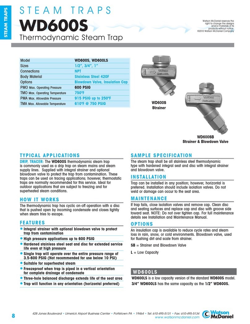
Watson McDaniel
Watson McDaniel WD600S Installation and maintenance manual
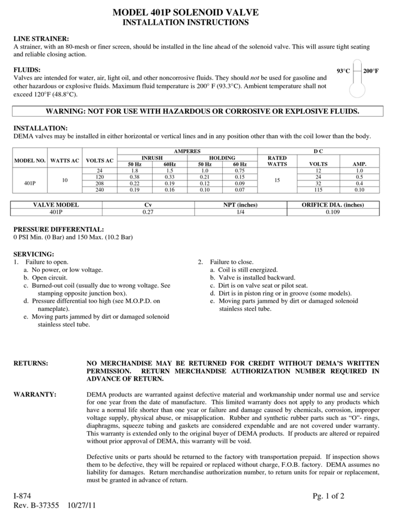
DEMA
DEMA 401P installation instructions
SYR
SYR ESBE VST100 Series manual
Grundfos
Grundfos PRV Series Installation and operating instructions

