MEIG SLM758 Guide
MeiG Smart product technical information
SLM758 Hardware Design Guide Page 1
SLM758 Hardware Design Guide
Released Date: 2018/11
File name: SLM758 Hardware Design Guide
Version Number: V1.08
Company: MeiG Smart Technology Co., Ltd

MeiG Smart product technical information
SLM758 Hardware Design Guide Page 2
IMPORTANT NOTICE
COPYRIGHT NOTICE
Copyright © MeiG Smart Technology Co., Ltd. All rights reserved.
All contents of this manual are exclusively owned by MeiG Smart Technology Co., Ltd(MeiG
Smart for short), which is under the protection of Chineselawsandcopyrightlaws in
international conventions. Anyone shall not copy, spread, distribute, modify or use in other
ways with its contents without the written authorization of MeiG Smart. Those
whoviolatedwillbe investigated by corresponding legal liability in accordance with the law.
NO GUARANTEE
MeiG Smart makes no representation or warranty, either express or implied, for any content
in this document, and will not be liable for any specific merchantability and applicable or any
indirect,particular and collateral damage.
CONFIDENTIALITY
All information contained here (including any attachments) is confidential. The recipient
acknowledges the confidentiality of this document, and except for the specific purpose, this
document shall not be disclosed to any third party.
DISCLAIMER
MeiG Smart will not take any responsibility for any property and health damage caused by
the abnormal operation of customers. Please develop the product according to the technical
specification and designing reference guide which defined in the product manual. MeiG
Smart have the right to modify the document according to technical requirement with no
announcement to the customer.

MeiG Smart product technical information
SLM758 Hardware Design Guide Page 3
SLM758 Hardware Design Guide_V1.08

MeiG Smart product technical information
SLM758 Hardware Design Guide Page 4
Foreword
Thank you for using the SLM758 module from Meg Smart. This product can provide data
communication services. Please read the user manual carefully before use, you will
appreciate its perfect function and simple operation method.
The company does not assume responsibility for property damage or personal injury caused
by improper operation of the user. Users are requested to develop the corresponding
products according to the technical specifications and reference designs in the manual. Also
pay attention to the general safety issues that mobile products should focus on.
Before the announcement, the company has the right to modify the contents of this manual
according to the needs of technological development.

MeiG Smart product technical information
SLM758 Hardware Design Guide Page 5
Contents
1. Introduction.......................................................................................................................................................... 8
2. Module overview.................................................................................................................................................. 8
2.1 Summary of features.................................................................................................................................... 10
2.2 Block diagram............................................................................................................................................. 12
3. Module Package..................................................................................................................................................... 13
3.1.Pin distribution diagram............................................................................................................................. 13
3.2. Pin definitions.............................................................................................................................................. 14
3.3. Mechanical Dimensions.............................................................................................................................. 30
4. Interface application.............................................................................................................................................. 31
4.1. Power Supply.............................................................................................................................................. 31
4.1.1. Power Pin................................................................................................................................................. 33
4.2. Power on and off......................................................................................................................................... 34
4.2.1. Module Boot............................................................................................................................................. 34
4.2.2. Module Shutdown.................................................................................................................................... 35
4.2.2.1 PWRKEY Shutdown............................................................................................................................. 35
4.2.3.Module Reset............................................................................................................................................. 36
4.3. VCOIN Power............................................................................................................................................. 37
4.4. Power Output.............................................................................................................................................. 38
4.5. Serial Port.................................................................................................................................................... 38
4.6. MIPI Interface............................................................................................................................................. 41
4.6.1. LCD Interface .......................................................................................................................................... 41
4.6.2.MIPI Camera Interface........................................................................................................................... 45
4.7.Resistive Touch Interface............................................................................................................................ 49
4.8.CapacitiveTouch Interface.......................................................................................................................... 49
4.9.Audio Interface ............................................................................................................................................ 49
4.9.1Receiver Interface Circuit......................................................................................................................... 50
4.9.2 Microphone receiving Circuit................................................................................................................. 50
4.9.3.Headphone Interface Circuit ................................................................................................................... 51
4.9.4.Speaker Interface Circuit......................................................................................................................... 52
4.9.5.I2S Interface.............................................................................................................................................. 53
4.10. USB Interface............................................................................................................................................ 53
4.10.1. USB OTG................................................................................................................................................ 54
4.11. Charging Interface.................................................................................................................................... 55
4.11.1. Charging Detection................................................................................................................................ 55
4.11.2. Charge Control ...................................................................................................................................... 55
4.11.3. BAT_CON_TEM................................................................................................................................... 55
4.12 UIM Card Interface................................................................................................................................... 56
4.13. SD Card Interface..................................................................................................................................... 57
4.14 I2C Bus Interface....................................................................................................................................... 57
4.15 Analog to Digital Converter (ADC).......................................................................................................... 58
4.16. PWM.......................................................................................................................................................... 58
4.17. Motor ......................................................................................................................................................... 58
4.18 Antenna Interface...................................................................................................................................... 59
4.18.1 Main Antenna.......................................................................................................................................... 59
4.18.2 DRX Antenna.......................................................................................................................................... 60
4.18.3 GPS Antenna........................................................................................................................................... 61
4.18.4 WiFi/BT antenna..................................................................................................................................... 61
5.PCB Layout............................................................................................................................................................. 63
5.1. Module PIN distribution............................................................................................................................ 63
5.2. PCB Layout Principles............................................................................................................................... 63
5.2.1. Antenna..................................................................................................................................................... 63
5.2.2 Power Supply............................................................................................................................................. 64
5.2.3. SIM Card.................................................................................................................................................. 64
5.2.4. MIPI.......................................................................................................................................................... 65
5.2.5. USB............................................................................................................................................................ 65
5.2.6.Audio.......................................................................................................................................................... 65
5.2.7. Other......................................................................................................................................................... 66

MeiG Smart product technical information
SLM758 Hardware Design Guide Page 6
6. Electrical, Reliability............................................................................................................................................. 67
6.1 Absolute Maximum...................................................................................................................................... 67
6.2 Working Temperature................................................................................................................................. 67
6.3 Working Voltage.......................................................................................................................................... 67
6.4 Digital Interface Features............................................................................................................................ 67
6.5 SIM_VDD Characteristics .......................................................................................................................... 68
6.6 PWRKEY Feature....................................................................................................................................... 68
6.7 VCOIN Feature............................................................................................................................................ 68
6.8 Current Consumption (VBAT = 3.8V)....................................................................................................... 68
6.9 Electrostatic Protection............................................................................................................................... 69
6.10 Module Operating Frequency Band......................................................................................................... 69
6.11 RF Characteristics..................................................................................................................................... 71
6.12 Module Conduction Receiving Sensitivity............................................................................................... 71
6.13 WIFI Main RF Performance .................................................................................................................... 72
6.14 BT Main RF Prformance .......................................................................................................................... 73
6.15 GNSS Main RF Performance ................................................................................................................... 73
7. Production.............................................................................................................................................................. 74
7.1. Top And Bottom Views Of The Module ................................................................................................... 74
7.2. Recommended Soldering Furnace Temperature Curve ......................................................................... 74
7.3. Humidity Sensitivity (MSL)....................................................................................................................... 74
7.4. Baking Requirements................................................................................................................................. 75
8. Support Peripheral Device List............................................................................................................................ 76
9. Appendix ................................................................................................................................................................ 78
9.1. Related Documents..................................................................................................................................... 78
9.2. Terms And Explanations............................................................................................................................ 78
9.3. Multiplexing function................................................................................................................................. 80
9.4. Safety Warning ........................................................................................................................................... 81
10. OEM/Integrators Installation Manual....................................................................................................... 81
10.1.Important Notice to OEM integrators............................................................................................. 81
10.2.End Product Labeling........................................................................................................................ 82
10.3.Manual Information to the End User............................................................................................... 82
10.4.Federal Communication Commission Interference Statement...................................................... 83
10.5.Industry Canada Statement.............................................................................................................. 83
10.6.Radiation Exposure Statement......................................................................................................... 84
MeiG Smart product technical information
SLM758 Hardware Design Guide Page 7
Version History
Date
Version
Change description
Author
2017-06-12
1.00
First edition
Zheng Lei
2017-08-15
1.01
Correction
Guo Qianghua
2017-11-01
1.02
Modify information
Zheng Lei
2017-11-01
1.03
Modify information
Zheng Lei
2018-1-5
1.04
Modify information
Zheng Lei
2018-6-14
1.05
Modify frequency band
information
Zheng Lei
2018-8-3
1.06
Add I2S and CBL
information
Zheng Lei
2018-9-6
1.07
Update image information
Zheng Lei
2018-11-21
1.08
Update information about
reset,GPS
Zheng Lei

MeiG Smart product technical information
SLM758 Hardware Design Guide Page 8
1. Introduction
This document describes the hardware application interface of the module, including the
connection of the circuit and the RF interface.It can help users quickly understand the interface
definition, electrical performance, and structural dimensions of the module.Combining this
document with other application documents, users can quickly use modules to design mobile
communication applications.
2.Module overview
SLM758 series core board, uses the MSM8953 of Qualcomm Snapdragon 600 series for its
main chip, and its CPU is made of 14nm FinFET, built in 64bit ARM, 8 cores Cortex A-53,
main frequency 2.0G processor, supporting LPDDR3 SDRAM memory.
Supporting board memory of 16GB/32GB global different mode multi-mode LTE intelligent
communication module.This module is suitable for broadband intelligent wireless
communication modules of TD-LTE/FDD-LTE/WCDMA/EVDO/TD-SCDMA/CDMA/GSM
network standards.
The working frequency band supported by SLM758 module is:
FDD-LTE: B2/4/5/7/12/13/17/28b
WCDMA: B2/4/5

MeiG Smart product technical information
SLM758 Hardware Design Guide Page 9
The SLM758 provides voice, SMS, address book, WiFi, BT and GPS functions while
providing high-speed broadband data access; Product supports dual 1300W 3D camera or depth
of field camera, and it can be widely used in VR Camera, intelligent robot, Video surveillance,
security, automotive equipment, intelligent platform handheld terminals and other products.
The physical interface of the module is a 272-pin pad that provides the following hardware
interfaces:
Four 1.8V UART serial ports, supporting four or two wires.
Main LCD(MIPI interface)+ Secondary LCD(MIPI interface).
LCD backlight interface.
Three-way Camera interface(MIPI data).
Flashlight interface.
A high-speed USB interface.
Two Audio input interface.
Three Audio output interface.
Two-way UIM card interface.
GPIO interface.
Six groups of I2C interfaces.
Two sets of SPI interfaces.
One TF card interface.
Support GNSS,WiFi,Bluetooth 4.1 functions.

MeiG Smart product technical information
SLM758 Hardware Design Guide Page 10
2.1 Summary of features
Table 2.1:SLM758 features
Product characteristics
Description
Plateform
Qualcomm MSM8953
CPU
Octa-core A53 (64bit) 8*2.0GHz
* Octa-core A53 (64bit) 8*1.8GHz
* Octa-core A53 (64bit) 8*2.2GHz
GPU
Adreno506;650MHz
System memory
16GB eMMC + 2GB LPDDR3 933Mhz compatible with 32GB+3GB
OS
Android 7.1
Size
45.5x41.0x3.0mm,160pin LCC+112pin LGA
Networkband
SLM758
FDD-LTE: B2/4/5/7/12/13/17/28b
WCDMA: B2/4/5
Wi-Fi
WCN3660B:IEEE 802.11b/g/n/a 2.4G&5G
Bluetooth
BT 4.1
GNSS
GPS/Beidou/Glonass/Galileo
Data
Access
TD-LTE
Cat4 TD-LTE 117/30Mbps
FDD-
LTE
Cat4 FDD-LTE 150/50Mbps
DC-
HSPA+
42/11.2Mbps
TD-
HSPA
2.8/2.3Mbps
EVDO
Rev.A
3.1/1.8Mbps
EDGE
Class12, 236.8kbps/236.8kbps
GPRS
Class12, 85.6kbps/85.6kbps
SIM
DSDS(Dual Sim-card Dual Stanby)
3.0/1.8V
Support SIM hot plug
L/W/G/T+G
L/W/G/T+W
L/W/G/T+1X
L/EVDO/CDMA1X+G
Don’t support dual CDMA SIM card
Display
((Home
screen/subscreen))
Matrix:
FULL HD: 1920*1200 60fps;
LCD Size: User defined
Interface: 1st LCM:MIPI DSI 4-lane; 2nd LCM:MIPI DSI 4-lane
Camera
(Front and Rear)
Interface: Support three sets of CSI, each group is 4-Lane
Camera
Pixel:Rear 13-24Mp/Front up to 13Mp,Dual ISP can support dual
MeiG Smart product technical information
SLM758 Hardware Design Guide Page 11
13MP Camera at the same time
Video decode
4K 30fps, 1080p 60fps, H.264/H.265 MP4/ WMV9/
VC1/ DivX/ VP8/VP9
Video encode
4K 30fps,1080p 60 fps: H.264/ H.265/ MP4/ VP8
1080P 60fps De +1080p 30fps En
Input Device
Key(Power on/off, Home, Volume+, Volume-)
Capacitive TP
Reset
Support HW reset
Application
interface
Interface name
Main function description
VBAT
3pin,Power input,3.4V~4.2V,Nominal
value3.8V
SDIO *1
TF Card,Support 128GB max
USB2.0(3.0)
Support OTG
USB_BOOT(Force USB boot for emergency
downloads)
BLSP ports
7 ports(BLSP2-8), 4-bits each, multiplexed serial
interface functions
UART*4
BLSP2,BLSP4-6 support UART,up to 4 Mbps
I2C*6
BLSP2-6&BLSP8 support I2C, These BLSPs use bits
[1:0] for I2C
SPI(master
only)
SPI is only support via BLSP
ADC*3
Support
Charge
Support5V/2A
Vibrator
Support
GPIO
25 GPIOs,Excluded BLSP multiplexing GPIO and
GPIO involved in LCM、TP and CAMERA
VCOIN
Real time clock backup battery
RF Interface
Multimode LTE main antenna
Multimode LTE diversity antenna
The GPS antenna
2.4G WiFi/BT antenna
5G WIFI- antenna
Audio
One main MIC
One noise reduction MIC
One Handsfree speaker(Built in 0.8W Class D
amplifier)
One earpiece
One stereo headphone(With headphone MIC)
One audio output
Two I2S signal

MeiG Smart product technical information
SLM758 Hardware Design Guide Page 12
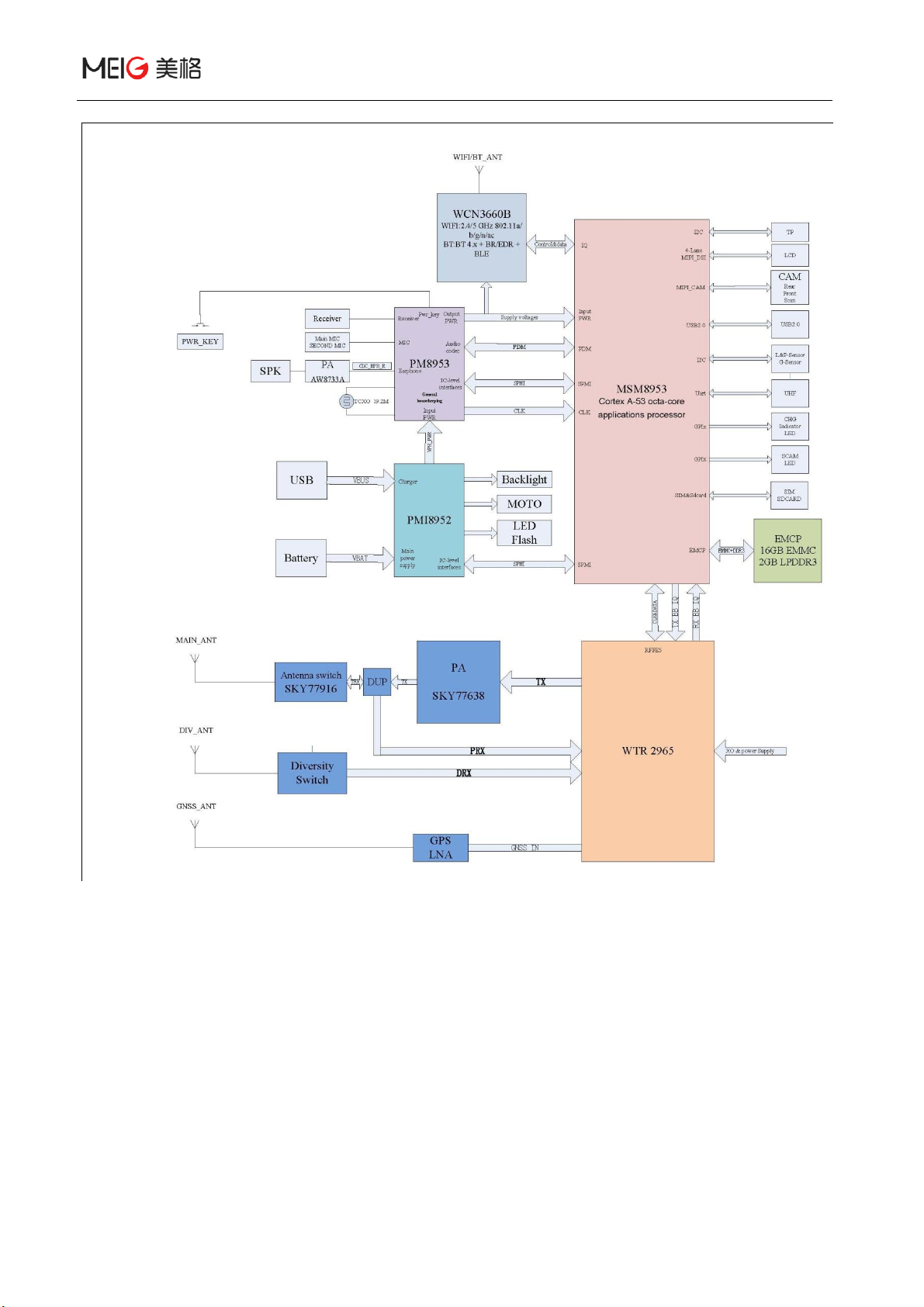
2.2 Block diagram
The following figure lists the main functional parts of the module:
MSM8953 baseband chip
PM8953 power management chip
PMI8952 power management chip
WCN3660B(Compatible with WCN3680B)-WIFI/BT/FM three in one chip
Antenna interface
LCD/CAM-MIPI interface
EMCP memory chip
AUDIO interface
UART、SD card interface,SIM card interface,I2Cinterface,etc.
MeiG Smart product technical information
SLM758 Hardware Design Guide Page 13
Figure 2.1: module function block diagram
3. Module Package
3.1.Pin distribution diagram

MeiG Smart product technical information
SLM758 Hardware Design Guide Page 14
Figure 3.1:module pin diagram (top view)
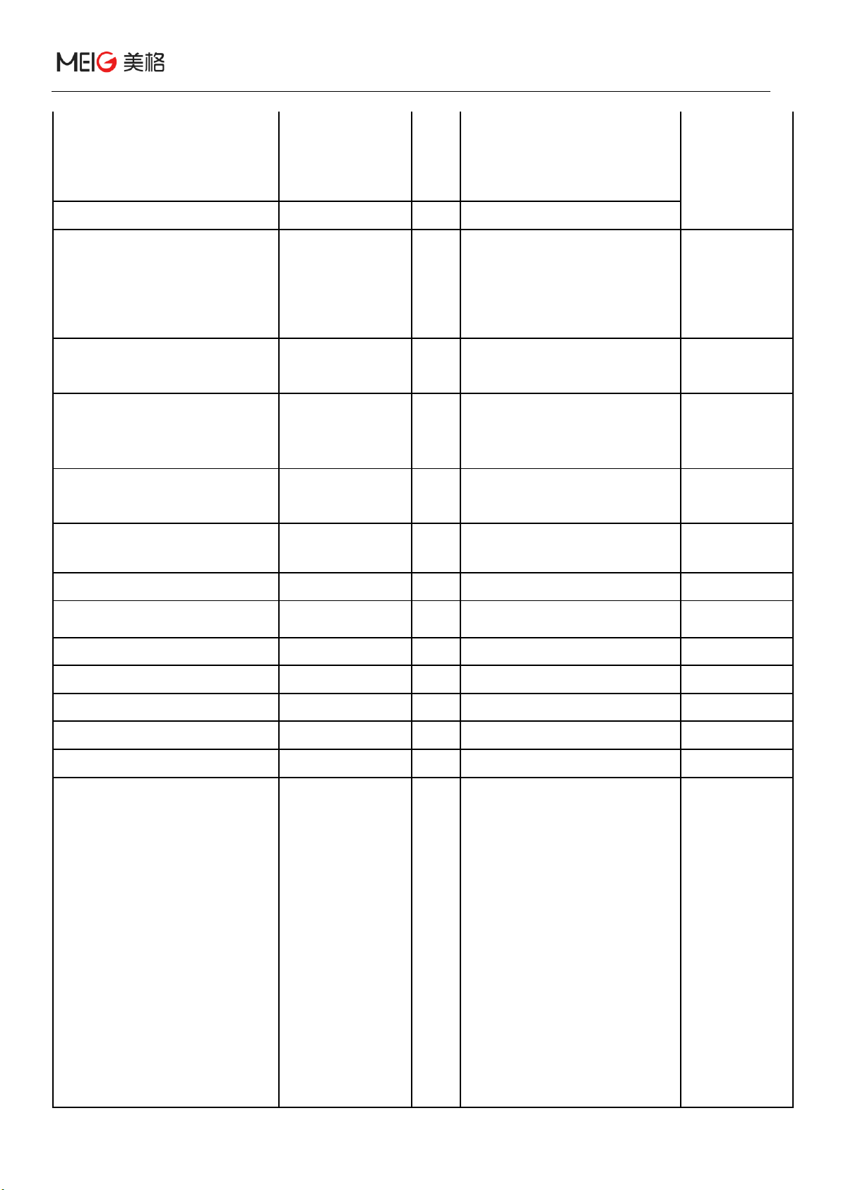
3.2. Pin definitions
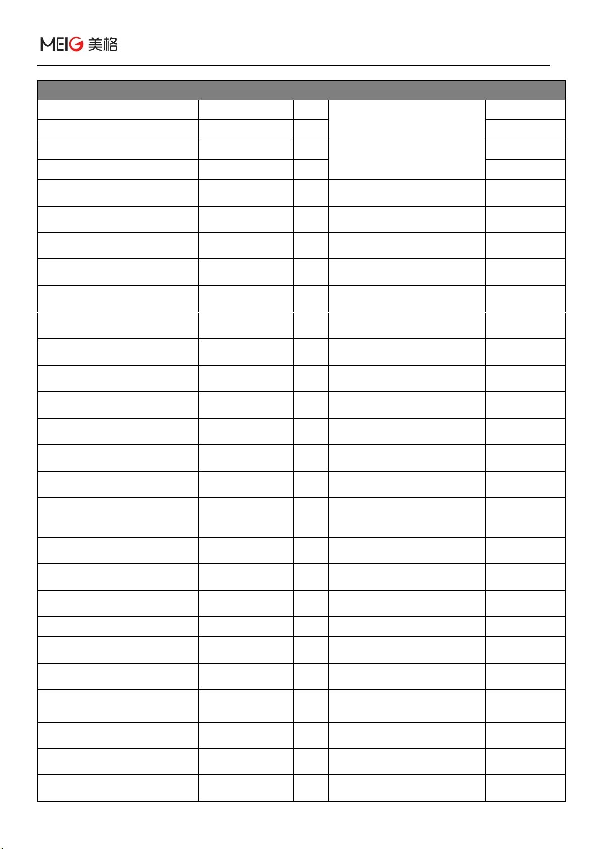
table 3.1:Pin description
Pin number
Pin number
I/O
Description
Comment
The power supply
MeiG Smart product technical information
SLM758 Hardware Design Guide Page 15
VBAT
151、152、153
I
The module provides three
VBAT power pin pins. The
SLM758 operates from a single
supply with a voltage range
from 3.4V to 4.2V for VBAT.
Externally,
capacitors and
Zener diodes
must be added
for surge
protection.
VBUS
157、158、159
I/O
5V charging input power.
VCOIN
113
I/O
When the VBAT of the system
power is absent, the external
backup battery provides power
to the system real-time
clock.When VBAT is present,
the backup battery is charged.
VCOIN pins
connect 3V
button batteries
or large
capacitors.
VREG_L5_1P8
140
O
1.8V power output, always
available for CPU, Memory, IO
and other power supply.
100mA
VREG_L6_1P8
139
O
1.8 V power output, standby will
be closed, used for Camera,
LCD and other small current
power supply.
100mA
VREG_L10_2P8_SENSOR
138
O
2.8V power output, will be
turned off during standby, used
for Sensor, TP power supply.
150mA
VREG_L17_2P85
137
O
2.85 V power output, for LCD,
C
400mA
VREG_L11_2P95
29
O
TF card power supply pin
500mA
VREG_L12_PX2_2P95
30
O
TF card signal pull-up power
supply pin
100mA
VREG_L14_UIM1
110
O
UIM power supply pins
50mA
VREG_L15_UIM2
91
O
UIM power supply pins
50mA
VREG_L22_2P8_AVDD
136
O
Camera AVDD
300mA
VREG_L2_1P1
199
O
Main Camera DVDD
300mA
VREG_L23_1P2_DVDD
200
O
Secondary camera DVDD
300mA
GND
1、3、10、23、
28、38、39、
48、57、68、
70、81、83、
92、94、101、
103、111、116、
119、121、135、
144、147、150、
154、155、156、
160、161、170、
175、180、181、
210、211、213、
214、215、216、
218、220、222、
223、224、252、
257、272
GND
MeiG Smart product technical information
SLM758 Hardware Design Guide Page 16
Main display interface (MIPI)
MIPI_DSI0_CLK_N
64
O
MIPI_LCD clock
MIPI_DSI0_CLK_P
65
O
MIPI_DSI0_LANE0_N
189
I/O
MIPI_LCD data
MIPI_DSI0_LANE0_P
190
I/O
MIPI_DSI0_LANE1_N
66
I/O
MIPI_DSI0_LANE1_P
67
I/O
MIPI_DSI0_LANE3_N
73
I/O
MIPI_DSI0_LANE3_P
74
I/O
MIPI_DSI0_LANE2_N
71
I/O
MIPI_DSI0_LANE2_P
72
I/O
GPIO61_LCD_RST_N
75
O
LCD reset
GPIO24_LCD_TE0
76
I/O
LCD frame sync signal
The main display backlight interface
LCD_BL_LED_K1
5
AI
LCD Series backlight negative1
Each normal
20mA,max
30mA
LCD_BL_LED_K2
6
AI
LCD Series backlight negative2
LCD_BL_LED_A
7
PO
LCD Series backlight positive
Sub display interface (MIPI)
MIPI_DSI1_CLK_N
242
O
MIPI_LCD2 clock
MIPI_DSI1_CLK_P
241
O
MIPI_DSI1_LANE0_N
226
I/O
MIPI_LCD2 data
MIPI_DSI1_LANE0_P
225
I/O
MIPI_DSI1_LANE1_N
240
I/O
MIPI_DSI1_LANE1_P
239
I/O
MIPI_DSI1_LANE2_N
244
I/O
MIPI_DSI1_LANE2_P
243
I/O
MIPI_DSI1_LANE3_N
246
I/O
MIPI_DSI1_LANE3_P
245
I/O
GPIO63_LCD2_RST_N
99
O
LCD2 reset
GPIO25_LCD_TE1
77
I/O
LCD2 frame sync signal
UART(1.8V)
UART2_MSM_TX
11
I
UART2 data transmit
UART2_MSM_RX
12
O
UART2 data receive
GPIO13_UART4_RX
16
O
UART4 data receive
GPIO12_UART4_TX
15
I
UART4 data transmit
GPIO17_UART5_RX
255
O
UART5 data receive
MeiG Smart product technical information
SLM758 Hardware Design Guide Page 17
GPIO16_UART5_TX
256
I
UART5 data transmit
GPIO21_UART6_RX
177
I
UART6 data receive
GPIO20_UART6_TX
176
O
UART6 data transmit
UIM card Interface
UIM1_DET
106
I
UIM1 insert detect
UIM1_RESET
107
O
UIM1 reset
UIM1_CLK
108
O
UIM1 clock
UIM1_DATA
109
I/O
UIM1 data
UIM2_DET
87
I
UIM2 insert detect
UIM2_RESET
88
O
UIM2 reset
UIM2_CLK
89
O
UIM2 clock
UIM2_DATA
90
I/O
UIM2 data
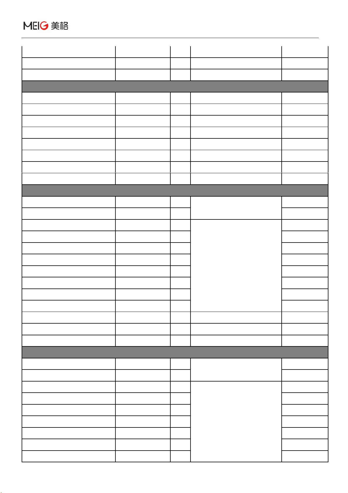
Front Camera
MIPI_CSI2_CLK_P
40
I
Front Camera MIPI clock
MIPI_CSI2_CLK_N
41
I
MIPI_CSI2_LANE0_P
42
I
Front Camera MIPI data
MIPI_CSI2_LANE0_N
43
I
MIPI_CSI2_LANE1_P
191
I
MIPI_CSI2_LANE1_N
192
I
MIPI_CSI2_LANE2_P
46
I
MIPI_CSI2_LANE2_N
47
I
MIPI_CSI2_LANE3_P
44
I
MIPI_CSI2_LANE3_N
45
I
GPIO27_SCAM_MCLK
80
I/O
Front Camera main clock
GPIO129_SCAM_RST_N
79
I/O
Front Camera reset
GPIO130_SCAM_PWD_N
78
I/O
Front Camera dormancy
Rear Camera
MIPI_CSI0_CLK_N
50
I
Rear Camera MIPI clock
MIPI_CSI0_CLK_P
49
I
MIPI_CSI0_LANE0_N
56
I
Rear Camera MIPI data
MIPI_CSI0_LANE0_P
55
I
MIPI_CSI0_LANE1_N
194
I
MIPI_CSI0_LANE1_P
193
I
MIPI_CSI0_LANE2_N
52
I
MIPI_CSI0_LANE2_P
51
I
MIPI_CSI0_LANE3_N
54
I

MeiG Smart product technical information
SLM758 Hardware Design Guide Page 18
MIPI_CSI0_LANE3_P
53
I
GPIO26_MCAM_MCLK
84
I/O
Rear Camera main clock
GPIO40_MCAM_RST_N
85
I/O
Rear Camera reset
GPIO39_MCAM_PWD_N
86
I/O
Rear Camera dormancy
Depth Camera
MIPI_CSI1_CLK_N
207
I
Depth Camera clock
MIPI_CSI1_CLK_P
208
I
MIPI_CSI1_LANE0_N
63
I
Depth Camera MIPI data
MIPI_CSI1_LANE0_P
62
I
MIPI_CSI1_LANE1_N
59
I
MIPI_CSI1_LANE1_P
58
I
MIPI_CSI1_LANE2_N
172
I
MIPI_CSI1_LANE2_P
171
I
MIPI_CSI1_LANE3_N
61
I
MIPI_CSI1_LANE3_P
60
I
GPIO132_DCAM_PWD_N
262
I/O
Depth Camera dormancy
GPIO131_DCAM_RST_N
263
I/O
Depth Camera reset
GPIO28_CAM_MCLK2
264
I/O
Depth Camera main clock
Audio Interface
MIC_IN1_M
123
I
The main MIC negative
MIC_IN1_P
122
I
The main MIC positive
MIC_IN2_P
132
I
Headphone MIC positive
GND_MIC
124
I
Headphone MIC、Noise
reduction MIC negative
MIC_IN3_P
131
I
Noise reduction MIC positive
MIC_BIAS1
118
O
The BIAS voltage of main MIC
is used in the design of silicon
wheat
MIC_BIAS2
117
O
The BIAS voltage of the
earphone MIC is used in the
design of silicon wheat
CDC_HPH_R
128
O
Right channel of earphone
CDC_HPH_L
126
O
Left channel of earphone
CDC_HS_DET
125
I
Headphone plug and unplug
detection
CDC_HPH_REF
127
I
Earphone reference GND
CDC_EAR_M
129
O
Earpiece output negative
CDC_EAR_P
130
O
Earpiece output positive
SPKR_DRV_M
133
O
Power amplifier (0.85 W) output
negative
Class_D
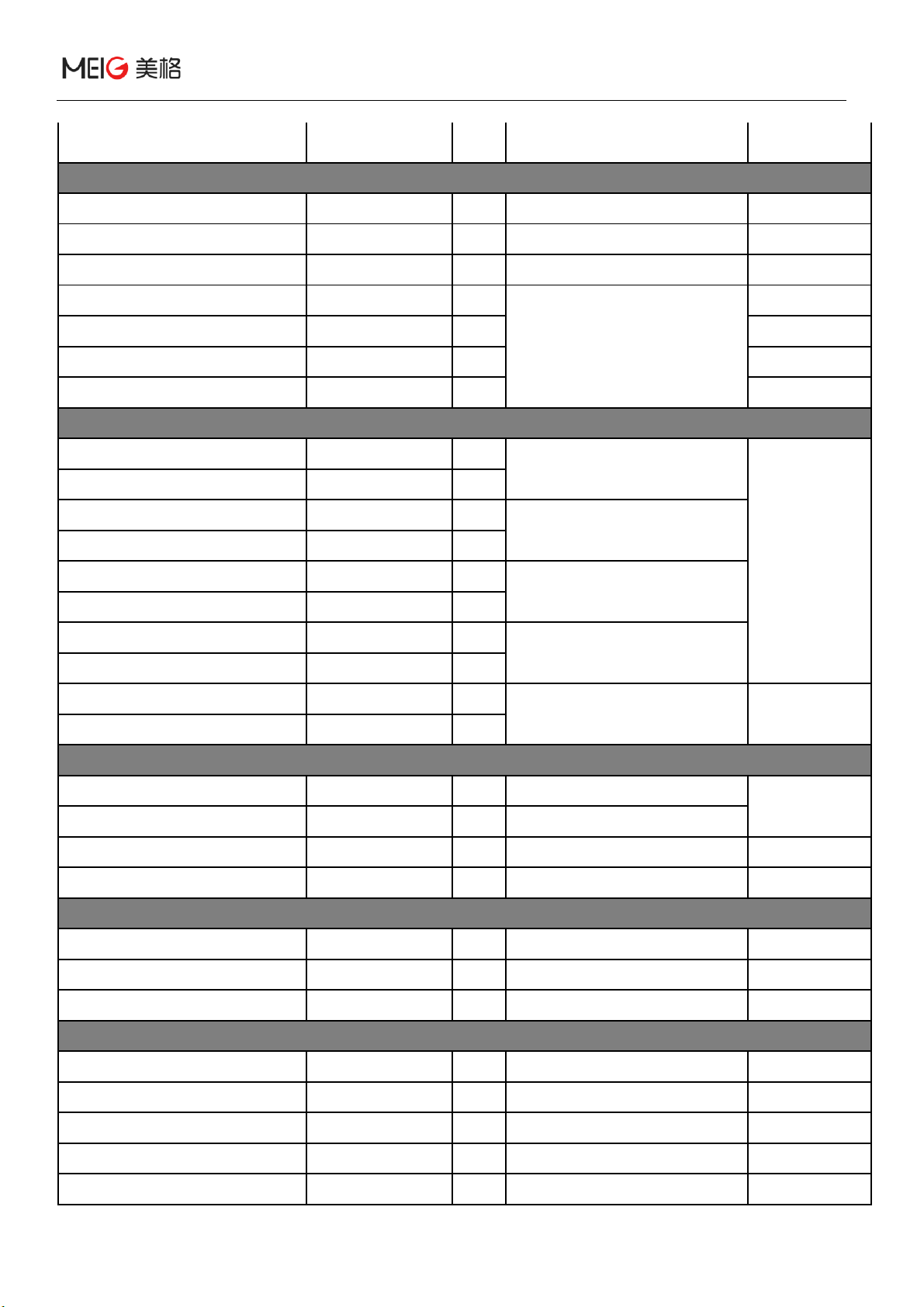
MeiG Smart product technical information
SLM758 Hardware Design Guide Page 19
SPKR_DRV_P
134
O
Power amplifier (0.85 W) output
positive
Class_D
SD card Interface
GPIO133_SDCARD_DET_N
31
I/O
SD card insertion detection
SDC2_SDCARD_CMD
36
I/O
SD CMD
SDC2_SDCARD_CLK
37
I/O
SD clock
SDC2_SDCARD_D0
32
I/O
SD data
SDC2_SDCARD_D1
33
I/O
SDC2_SDCARD_D2
34
I/O
SDC2_SDCARD_D3
35
I/O
I2C
CAM_I2C_SDA0
105
I/O
Special I2C signal can only be
used for CAM
Pullup to
VREG_L6_1P
8
CAM_I2C_SCL0
104
I/O
GPIO14_SENSOR_I2C4_SDA
17
I/O
Special I2C signal can only be
used for SENSOR
GPIO15_SENSOR_I2C4_SCL
18
I/O
GPIO6_I2C2_SDA
13
I/O
Universal I2C signal
GPIO7_I2C2_SCL
14
I/O
CAM_I2C_SDA1
96
I/O
Special I2C signal can only be
used for CAM
CAM_I2C_SCL1
95
I/O
GPIO18_NFC_I2C5_SDA
254
I/O
Universal I2C signal, which is
used by default for NFC
Pullup to
VREG_L5_1P
8
GPIO19_NFC_I2C5_SCL
253
I/O
TP
GPIO10_TP_I2C3_SDA
234
I/O
I2C data
Pullup to
VREG_L5_1P
8
GPIO11_TP_I2C3_SCL
233
I/O
I2Cclock
GPIO65_TP_INT_N
97
I
TP interrupt
GPIO64_TP_RST_N
98
O
TP reset
USB
USB_HS_D_M
145
I/O
USB DM
USB_HS_D_P
146
I/O
USB DP
USB_ID
143
I
USB ID
Antenna interface
RF_MAIN
120
I/O
The main antenna
RF_WIFI/BT
82
I/O
WIFI/BT antenna
RF_DIV
102
I
Diversity antenna
RF_GPS
93
I
GPS antenna
5G_ANT
69
I/O
5GWIFI antenna
MeiG Smart product technical information
SLM758 Hardware Design Guide Page 20
GPIOand default function
GPIO0_SPI_MOSI
261
O
The default configuration is the
SPI interface
GPIO1_SPI_MISO
260
O
GPIO2_SPI1_CS
259
I
GPIO3_SPI1_CLK
258
O
GPIO8
232
I/O
Generic GPIO, without default
configuration
GPIO9
231
I/O
Generic GPIO, without default
configuration
GPIO33
166
I/O
Generic GPIO, without default
configuration
GPIO35
167
I/O
Generic GPIO, without default
configuration
GPIO36
168
I/O
Generic GPIO, without default
configuration
GPIO38
251
I/O
The default configuration is the
gyroscope interrupt signal.
GPIO42_ACCL_INT1
19
I/O
The default configuration is G-
sensor interrupt
GPIO43_ALSP_INT_N
20
I/O
The default configuration is Ps-
sensor interrupt signal
GPIO44_MAG_INT
21
I/O
The default configuration is the
compass interrupt signal.
GPIO45_GYRO_INT
22
I/O
The default configuration is the
gyroscope interrupt signal.
GPIO46_PRESSURE_INT
221
I/O
The default configuration is the
pressure sensor interrupt signal
GPIO47
235
I/O
Generic GPIO, without default
configuration
GPIO48_FP_INT_N
270
I/O
The default configuration is the
interrupt signal for fingerprint
recognition.
GPIO59
100
I/O
General purpose GPIO, no
default configuration
GPIO63
99
I/O
General purpose GPIO, no
default configuration
GPIO66
212
I/O
General purpose GPIO, no
default configuration
GPIO85_KEY1_VOL+
24
I/O
Control volume increase
GPIO86_KEY2_SNAPSHOT
25
I/O
The default configuration is the
button
GPIO87_KEY3_FOCUS
26
I/O
The default configuration is the
button
GPIO88_KEY4_HOME
27
I/O
HOME key,Compatible with
MI2S_1_D1
GPIO89_DMIC0_CLK
204
I/O
General purpose GPIO, no
default configuration
GPIO90_DMIC0_DATA
205
I/O
General purpose GPIO, no
default configuration
GPIO96_WSA_EN
197
I/O
The default configuration is
AUDIO enable signal
Table of contents
Other MEIG Control Unit manuals


Popular Control Unit manuals by other brands


Siemens
Siemens 3WN 6 3WX3661-0JA00 operating instructions

IBASE Technology
IBASE Technology ET876 Series user manual

Fuji Electric
Fuji Electric MICREX-SX Series SPH user manual

tempLED
tempLED RayTrack Multisensor installation guide

Watts
Watts HKF20 Series Installation and operating manual

Gefa
Gefa Domino AT 100 Series Instructions for use

Bosch
Bosch Rexroth IndraControl XFE 01.1 Series operating instructions

FarmTronics
FarmTronics ChickenMaster user guide

SSS Siedle
SSS Siedle BMM 611-0 Product information

Faraday
Faraday 8706 INSTALLATION INSTRUCTIONS AND WIRING

Advanced Energy
Advanced Energy Thyro-PX Anybus Guide

SMC Networks
SMC Networks VM1000 Series instruction manual