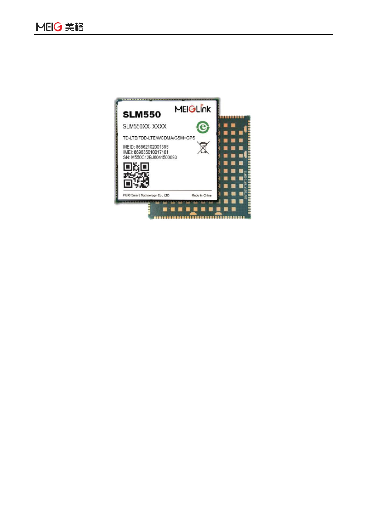
MeiG_SLM550_Hardware Design Manual
MeiG Smart Technology Co., Ltd 8/89
Contents
Important Notice ....................................................................................................................................... 1
Revision History ....................................................................................................................................... 2
SLM550 Hardware Design Guide_V1.02................................................................................................. 3
Contents .................................................................................................................................................... 6
1 Introduction.......................................................................................................................................... 8
2 Module overview ................................................................................................................................. 9
2.1 Summary of features ................................................................................................................... 9
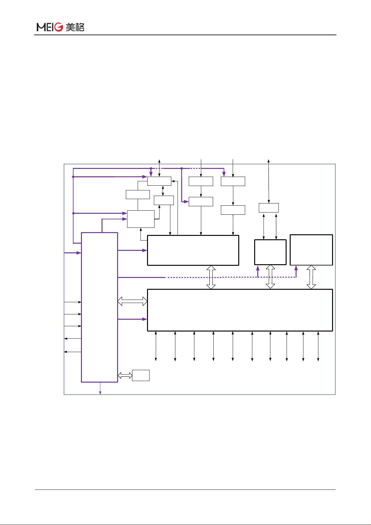
2.2 Block diagram ........................................................................................................................... 11
3 Module Package ................................................................................................................................ 13
3.1 Pin distribution diagram ............................................................................................................ 13
3.2 Pin definitions ............................................................................................................................ 14
3.3 Mechanical Dimensions ............................................................................................................ 34
4 Interface application ......................................................................................................................... 36
4.1 Power Supply ............................................................................................................................ 36
4.1.1 Power Pin........................................................................................................................ 37
4.2 Power on and off ....................................................................................................................... 37
4.2.1 Module Boot .................................................................................................................... 37
4.2.2 Module Shutdown ........................................................................................................... 39
4.2.3 Module Reset .................................................................................................................. 39
4.3 VCOIN Power ............................................................................................................................ 40
4.4 Power Output ............................................................................................................................ 41
4.5 Serial Port ................................................................................................................................. 42
4.6 MIPI Interface ............................................................................................................................ 44
4.6.1 LCD Interface .................................................................................................................. 44
4.6.2 MIPI Camera Interface .................................................................................................. 46
4.7 Capacitive Touch Interface ........................................................................................................ 50
4.8 Audio Interface .......................................................................................................................... 51
4.8.1 Receiver Interface Circuit ............................................................................................... 52
4.8.2 Microphone receiving Circuit .......................................................................................... 52
4.8.3 Headphone Interface Circuit ........................................................................................... 52
4.8.4 LINE OUT Circuit ............................................................................................................ 53
4.8.5 I2S Interface ................................................................................................................... 53
4.9 USB Interface ............................................................................................................................ 54
4.9.1 USB OTG ........................................................................................................................ 56
4.10 Charging Interface ................................................................................................................... 56
4.10.1 Charging Detection ....................................................................................................... 57
4.10.2 Charge Control ............................................................................................................. 57
4.10.3 BAT_CON_TEM ........................................................................................................... 57
4.11 UIM Card Interface ................................................................................................................... 58
4.12 SD Card Interface .................................................................................................................... 59
4.13 I2C Bus Interface ..................................................................................................................... 59
4.14 Analog to Digital Converter (ADC) ........................................................................................... 60
4.15 PWM......................................................................................................................................... 60
4.16 Motor ........................................................................................................................................ 61