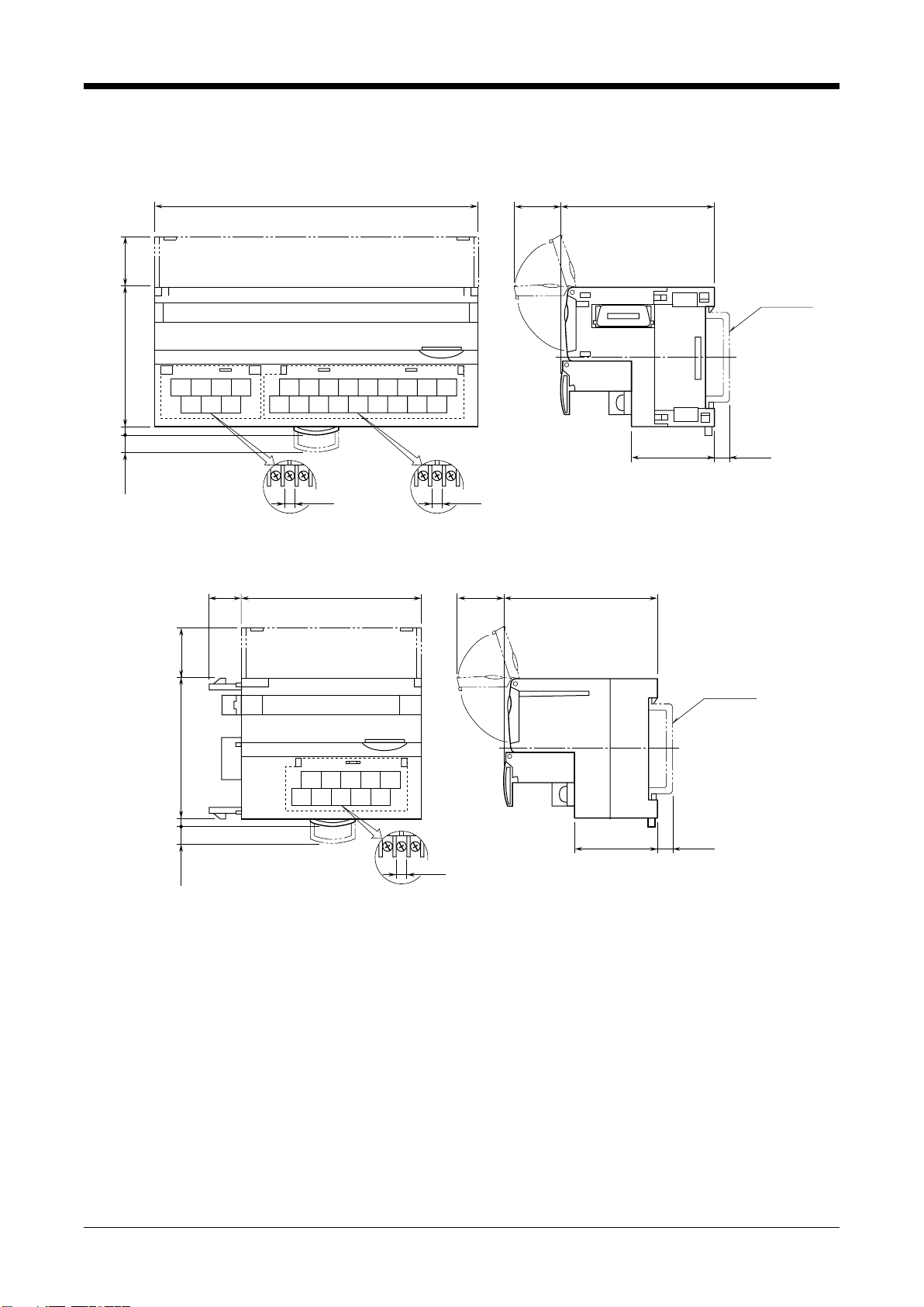
MG R7MWTU User manual

EM-7816 Rev.4 P. 1 / 20
MG CO., LTD. www.mgco.jp
5-2-55 Minamitsumori, Nishinari-ku, Osaka 557-0063 JAPAN
INSTRUCTION MANUAL
MULTI POWER MONITORING MODULE
(clamp-on current sensor CLSE, Modbus) MODEL R7MWTU
BEFORE USE ....
Thank you for choosing us. Before use, please check con-
tents of the package you received as outlined below.
If you have any problems or questions with the product,
please contact our sales office or representatives.
■PACKAGE INCLUDES:
Multi power monitoring module or extension module ......(1)
Terminating resistor (110Ω, 0.25W) ..................................(1)
■MODEL NO.
Confirm Model No. marking on the product to be exactly
what you ordered.
■INSTRUCTION MANUAL
This manual describes necessary points of caution when
you use this product, including installation, connection and
basic maintenance procedures.
The R7MWTU is programmable by using the PC Configura-
tor Software. For detailed information on the PC configura-
tion, refer to the PMCFG users manual. The PMCFG PC
Configurator Software is downloadable at our web site.
POINTS OF CAUTION
■POWER INPUT RATING & OPERATIONAL RANGE
• Locate the power input rating marked on the product and
confirm its operational range as indicated below:
100 – 240V AC rating: 85 – 264V, 50/60 Hz,
Basic module <5VA
Basic module + Extension module < 6VA
110 – 240V DC rating: 99 – 264V,
Basic module <1.5W
Basic module + Extension module < 2W
■GENERAL PRECAUTIONS
• Before you remove or mount the unit, turn off the power
supply and input signal for safety.
■ENVIRONMENT
• Indoor use.
• When heavy dust or metal particles are present in the
air, install the unit inside proper housing with sufficient
ventilation.
• Do not install the unit where it is subjected to continuous
vibration. Do not subject the unit to physical impact.
• Environmental temperature must be within -10 to +55°C
(14 to 131°F) with relative humidity within 30 to90% RH
in order to ensure adequate life span and operation.
■WIRING
• Wiring to the unit must be conducted by qualified service
personnel.
• Do not install cables close to noise sources (relay drive
cable, high frequency line, etc.).
• Do not bind these cables together with those in which
noises are present. Do not install them in the same duct.
■AND ....
• The unit is designed to function as soon as power is sup-
plied, however, a warm up for 10 minutes is required for
satisfying complete performance described in the data
sheet.

R7MWTU
EM-7816 Rev.4 P. 2 / 20
MG CO., LTD. www.mgco.jp
5-2-55 Minamitsumori, Nishinari-ku, Osaka 557-0063 JAPAN
COMPONENT IDENTIFICATION
■BASIC MODULE
5
4
3
2
1
0
9
8
7
6
5
4
3
2
1
0
9
8
7
6
5
4
3
2
1
0
9
8
7
6
ERR RD
RUN SD
PWR X10 X1
NODE ADD. B.RATE
CNFG.
12345678
4567
123
10 11 12 13
2341
15 16 17 18
7896
14
5
Baud Rate Setting Rotary SW
Node Address Setting
Rotary SW
Status Indicator LED
Operating Mode Setting DIP SW (SW1)
PC Configurator Jack
Modbus, Power Supply
Terminals Voltage, Current, Discrete Input Terminals
■EXTENSION MODULE
Input Terminals
786910
23145
■STATUS INDICATOR LED
ID COLOR S TAT U S FUNCTION
PWR Red ON Normal
Blinking
approx. 0.5 Hz
Input overload or no input
Blinking
approx. 2 Hz
Setting error or device
error
OFF Error in the internal 5V
RUN Red ON Normal communication
ERR Red ON Received data error
SD Red ON Data transmitting
RD Red ON Data receiving
■NODE ADDRESS
Node Address is selected between 1 and 99 in decimal. The
left switch determines the tenth place digit, while the right
switch does the ones place digit of the address.
5
4
3
2
1
0
9
8
7
6
5
4
3
2
1
0
9
8
7
6
Node Address Setting (x1)
Factory setting : 00
Node Address Setting (x10)
■BAUD RATE
Baud Rate is selected with the rotary switch.
(4 to 9 are unused. Be sure to set between 0 and 3)
5
4
3
2
1
0
9
8
7
6
Baud Rate Setting
0 : 38.4 kbps (factory setting)
1 : 19.2 kbps
2 : 9600 bps
3 : 4800 bps

R7MWTU
EM-7816 Rev.4 P. 3 / 20
MG CO., LTD. www.mgco.jp
5-2-55 Minamitsumori, Nishinari-ku, Osaka 557-0063 JAPAN
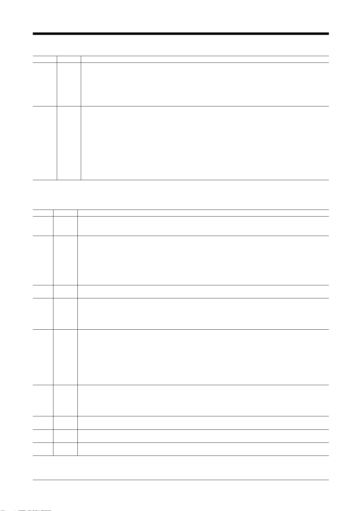
■OPERATING MODE SETTING
(*) Factory setting
• System Conguration (SW1-1, 2)
SW1-1 SW1-2 SYSTEM CONFIGURATION
OFF OFF Three-phase / 3-wire (*)
ON OFF Single-phase / 2-wire
OFF ON Single-phase / 3-wire
ON ON Three-phase / 4-wire
• Balanced or Unbalanced Load (SW1-3)
SW1-3 BALANCED / UNBALANCED
OFF Unbalanced (*)
ON Balanced
• Clamp Sensor Type (SW1-4, 5, 6)
Clamp sensor type setting is common to all circuits.
The sensor type and other settings for individual circuit is
available with the PC Configurator.
SW1-4 SW1-5 SW1-6 CLAMP SENSOR TYPE
OFF OFF OFF CLSE-R5 (5A) (*)
ON OFF OFF CLSE-05 (50A)
OFF ON OFF CLSE-10 (100A)
OFF OFF ON CLSE-20 (200A)
ON ON OFF CLSE-40 (400A)
OFF ON ON CLSE-60 (600A)
• Conguration Mode (SW1-8)
SW1-8 CONFIGURATION MODE
OFF DIP switch setting (*)
(PC Configurator setting is not available)
ON PC Configurator and communication
(DIP switch setting is not available)
Note 1: Turn on the power supply to the unit after setting node
address, baud rate and operating mode.
Note 2: Be sure to set unused SW1-7 to OFF.
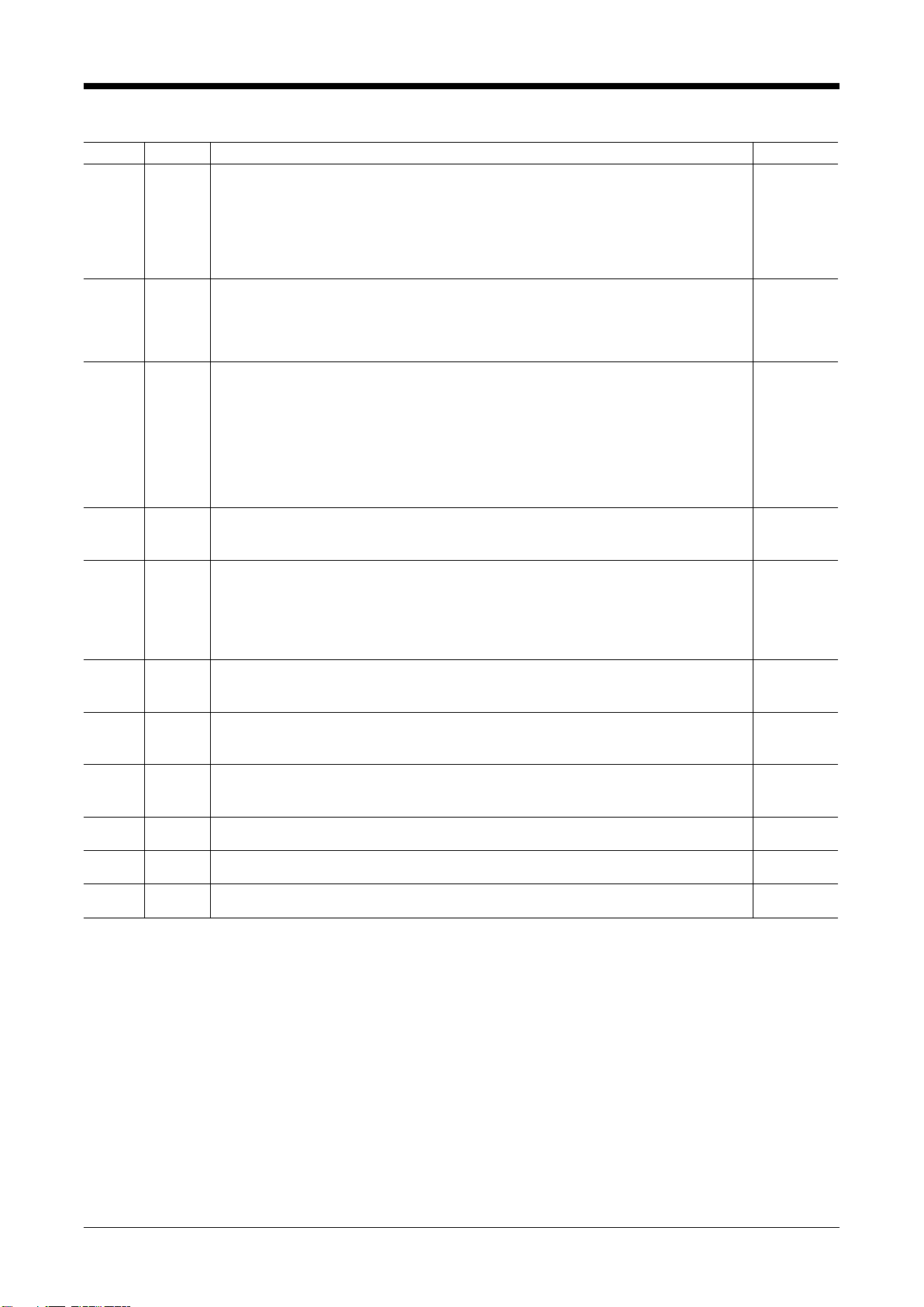
■POWER SUPPLY, MODBUS TERMINAL ASSIGNMENT
4
DA
5
DG
6
U(+)
1
DB
2
SLD
3
FG
7
V(−)
1. DB −
2. SLD Shield
3. FG FG
4. DA −
5. DG −
6. U(+) Power input (+)
7. V(−) Power input (−)
■INPUT TERMINAL ASSIGNMENT
lBASIC MODULE
• 1 Circuit, 4-point Discrete Input
•1Circuit, 4-point Discrete Inputs
14
56
2K
2L 3L
15
3K
16 17 18
78 9
DI1
+
DI3
+
COM
DI2
+
DI4
+
10
12
P3
P1 P2
11
NC
12 13
34
1ch
1ch 1ch
1ch1ch
1ch
NC 1K
N1L
COM
1P1 Voltage Input P1 10 P3 Voltage Input P3
2P2 Voltage Input P2 11 NC Unused
3NVoltage Input N12NC Unused
4
1ch 1L Ch.1, Current input 1L
13
1ch 1K Ch.1, Current input 1K
5
1ch 2L Ch.1, Current input 2L
14
1ch 2K Ch.1, Current input 2K
6
1ch 3L Ch.1, Current input 3L
15
1ch 3K Ch.1, Current input 3K
7 DI2 + Discrete input 216 DI1 + Discrete input 1
8 DI4 + Discrete input 417 DI3 + Discrete input 3
9 COM
Discrete input common
18 COM
Discrete input common
•2Circuits
14
56
2K
2L 3L
15
3K
16 17 18
78 9
10
12
P3
P1 P2
11
NC
12 13
34
1ch
1ch1ch
1ch1ch
1ch
NC 1K
N1L
2K
2L 3L
3K
2ch
2ch2ch
2ch2ch
2ch
1K
1L
1P1 Voltage Input P1 10 P3 Voltage Input P3
2P2 Voltage Input P2 11 NC Unused
3NVoltage Input N12NCUnused
4
1ch 1L Ch.1, Current input 1L
13
1ch 1K Ch.1, Current input 1K
5
1ch 2L Ch.1, Current input 2L
14
1ch 2K Ch.1, Current input 2K
6
1ch 3L Ch.1, Current input 3L
15
1ch 3K Ch.1, Current input 3K
7
2ch 1L Ch.2, Current input 1L
16
2ch 1K Ch.2, Current input 1K
8
2ch 2L Ch.2, Current input 2L
17
2ch 2K Ch.2, Current input 2K
9
2ch 3L Ch.2, Current input 3L
18
2ch 3K Ch.2, Current input 3K
No. ID FUNCTION No. FUNCTIONID
• 2 Circuits
•1Circuit, 4-point Discrete Inputs
14
56
2K
2L 3L
15
3K
16 17 18
78 9
DI1
+
DI3
+
COM
DI2
+
DI4
+
10
12
P3
P1 P2
11
NC
12 13
34
1ch
1ch 1ch
1ch1ch
1ch
NC 1K
N1L
COM
1P1 Voltage Input P1 10 P3 Voltage Input P3
2P2 Voltage Input P2 11 NC Unused
3NVoltage Input N12NC Unused
4
1ch 1L Ch.1, Current input 1L
13
1ch 1K Ch.1, Current input 1K
5
1ch 2L Ch.1, Current input 2L
14
1ch 2K Ch.1, Current input 2K
6
1ch 3L Ch.1, Current input 3L
15
1ch 3K Ch.1, Current input 3K
7 DI2 + Discrete input 216 DI1 + Discrete input 1
8 DI4 + Discrete input 417 DI3 + Discrete input 3
9 COM
Discrete input common
18 COM
Discrete input common
•2Circuits
14
56
2K
2L 3L
15
3K
16 17 18
78 9
10
12
P3
P1 P2
11
NC
12 13
34
1ch
1ch1ch
1ch1ch
1ch
NC 1K
N1L
2K
2L 3L
3K
2ch
2ch2ch
2ch2ch
2ch
1K
1L
1P1 Voltage Input P1 10 P3 Voltage Input P3
2P2 Voltage Input P2 11 NC Unused
3NVoltage Input N12NCUnused
4
1ch 1L Ch.1, Current input 1L
13
1ch 1K Ch.1, Current input 1K
5
1ch 2L Ch.1, Current input 2L
14
1ch 2K Ch.1, Current input 2K
6
1ch 3L Ch.1, Current input 3L
15
1ch 3K Ch.1, Current input 3K
7
2ch 1L Ch.2, Current input 1L
16
2ch 1K Ch.2, Current input 1K
8
2ch 2L Ch.2, Current input 2L
17
2ch 2K Ch.2, Current input 2K
9
2ch 3L Ch.2, Current input 3L
18
2ch 3K Ch.2, Current input 3K
No. ID FUNCTION No. FUNCTIONID
lEXTENSION MODULE
10
5
DI7+
DI8+
6
12
COM
COM DI2+
7
DI1+
89
34
DI3+ DI5+
DI4+
DI6+
1 COM Common 6 COM Common
2 DI2+ Discrete Input 2 7 DI1+ Discrete Input 1
3 DI4+ Discrete Input 4 8 DI3+ Discrete Input 3
4 DI6+ Discrete Input 6 9 DI5+ Discrete Input 5
5 DI8+ Discrete Input 8 10 DI7+ Discrete Input 7
■EXTENSION MODULE
No. ID FUNCTION No. FUNCTIONID

R7MWTU
EM-7816 Rev.4 P. 4 / 20
MG CO., LTD. www.mgco.jp
5-2-55 Minamitsumori, Nishinari-ku, Osaka 557-0063 JAPAN
TERMINAL CONNECTIONS
Connect the unit as in the diagram below.
■EXTERNAL DIMENSIONS unit: mm (inch)
l BASIC MODULE
4567
123
10 11 12 13
2341
15 16 17 18
789
6
14
5
30 (1.18) [5 (.20)]
3 (.12)5.5 (.22)
DIN RAIL
35mm wide
54 (2.13)
17 (.66)
50 (1.97) 18.5 (.73)
115 (4.53)
7–M3 SCREW TERMINALS
for Modbus, Power
18–M3 SCREW TERMINALS
for Voltage, Current, Discrete Input
6 (.24) 6 (.24)
l EXTENSION MODULE
11.5
(.45)
786910
23145
65 (2.56)
30 (1.18) [5 (.20)]
3 (.12)5.5 (.22)
DIN RAIL
35mm wide
54 (2.13)
17 (.66)
50 (1.97) 18.5 (.73)
10–M3 SCREW TERMINALS
for
Discrete Input
6 (.24)

R7MWTU
EM-7816 Rev.4 P. 5 / 20
MG CO., LTD. www.mgco.jp
5-2-55 Minamitsumori, Nishinari-ku, Osaka 557-0063 JAPAN
■CONNECTION DIAGRAM
l BASIC MODULE
VOLTAGE
INPUT
CURRENT
INPUT
DISCRETE
INPUT
Di1+
COM
COM
Di2+
Di3+
Di4+
• Discrete input connection e.g.
1
5
10
2
6
4
7
13
8
9
14
12
15
11
16
17
18
P1
P3
N
1L
2L
3L
DI2+
DI4+
COM
NC
COM
NC
1K
2K
3K
DI1+
DI3+
P2
3
• 1 Circuit, 4-point Discrete Input
TO OTHER
Modbus
DEVICES
4
1
2
5
3
DA
DB
DG
SLD
FG
6
7
U(+)
V(–)
POWER INPUT
1
5
10
2
6
4
7
13
8
9
14
12
15
11
16
17
18
P1
P3
N
1L
2L
3L
NC
NC
1K
2K
3K
1L
2L
3L
1K
2K
3K
P2
3
• 2 Circuits
VOLTAGE
INPUT
1ch. CURRENT
INPUT
2ch. CURRENT
INPUT
TO OTHER
Modbus
DEVICES
4
1
2
5
3
DA
DB
DG
SLD
FG
6
7
U(+)
V(–)
POWER INPUT
EXT. CONNECTOR
l EXTENSION MODULE
1
5
2
4
7
8
9
10
DI4+
DI6+
DI8+
DI1+
DI3+
DI5+
DI7+
■EXTENSION MODULE
DI2+
3
COM
6
COM
EXTENSION CONNECTOR

R7MWTU
EM-7816 Rev.4 P. 6 / 20
MG CO., LTD. www.mgco.jp
5-2-55 Minamitsumori, Nishinari-ku, Osaka 557-0063 JAPAN
■INPUT WIRING
1K 1L 3K 3L
source load
kl
P1
uv
UV
P2
uv
UV
P3
uv
UV
N
KL kl
KL
P1 P2 P3 1K 1L 3K 3LN
source load
kl
KL kl
KL
2K 2L
kl
KL
N
N
2K 2L
kl
KL
P1 N 1K 1L
source load
kl
KL
uv
UV
P1 N 1K 1L
source load
N
kl
KL
N
Three-phase /
4-wire,
balanced load
Three-phase /
4-wire,
unbalanced load
P1 P2 P3 1K 1L 3K 3L
L1
source load
N / L2
L3
uv vu
UV VU
kl
KL
kl
KL
P1 P2 P3 1K 1L 3K 3L
L1
source load
N / L2
L3
kl
KL
kl
KL
P1 P2 P3 1K 1L
source load
uv vu
UV VU
kl
KL
P1 P2 P3 1K 1L
L1
source load
L2
L3
kl
KL
P1 P2 1K 1L
L1
source load
N
kl
KL
uv
UV
P1 P2 1K 1L
L1
source load
N
kl
KL
System /
Application
Single-phase /
2-wire
Three-phase /
3-wire,
balanced load
Caution: Use CLSE for CT.
Grounding is unnecessary for low-voltage circuit.
Single-phase /
3-wire
Three-phase /
3-wire
unbalanced load
(2CT)
Terminal System /
Application Terminal
L1
L2
L3
L1
L2
L3
L1
L2
L3
L1
L2
L3
L1
L2
L3
COMMUNICATION CABLE CONNECTIONS
■MASTER CONNECTION
Tx+/Rx+
Tx–/Rx–
SG
Rx+
Rx–
Host PC
DA
DB
DG
SLD
FG
Remote Unit
DA
DB
DG
SLD
FG
Remote Unit
TERMINATOR TERMINATOR
Be sure to connect the terminating resistor included in the product package to the unit at both ends of transmission line.
The terminator must be connected across DA and DB.
The Host PC can be located other than at the extreme ends of transmission line.

R7MWTU
EM-7816 Rev.4 P. 7 / 20
MG CO., LTD. www.mgco.jp
5-2-55 Minamitsumori, Nishinari-ku, Osaka 557-0063 JAPAN
WIRING INSTRUCTIONS
■SCREW TERMINAL
Torque: 0.5 N·m
■SOLDERLESS TERMINAL
Refer to the drawing below for recommended ring tongue
terminal size. Spade tongue type is also applicable.
Applicable wire size: 0.25 to 1.65 mm2(AWG 22 to 16)
Recommended manufacturer: Japan Solderless Terminal
MFG. Co., Ltd, Nichifu Co., Ltd
6 (.24) max
3.3 (.13) max
mm (inch)
EXTENSION MODULE
A ‘basic’ module (Model: R7MWTU-221-AD4) can be at-
tached with one ‘extension’ module. The extension module
is powered from the basic module.
By combining two modules, single station can handle mixed
2 circuits power and discrete inputs.
Turn the power on after the extension module is connected.
CONNECTING THE EXTENSION MODULE
1) Remove the extension connector cover located at the
side of the basic module.
2) Connect the extension module.
3) Mount the combined module on a DIN rail.

R7MWTU
EM-7816 Rev.4 P. 8 / 20
MG CO., LTD. www.mgco.jp
5-2-55 Minamitsumori, Nishinari-ku, Osaka 557-0063 JAPAN
MODBUS - BASICS
This device conforms with Modbus-RTU protocol (MODBUS APPLICATION PROTOCOL V1.1a / Modbus over Serial Line
Specification & Implementation Guide V1.0).
The following communication parameters are selectable.
COMM. PROPERTY SELECTION
Modbus address 1 to 99
Baud rate 4800 bps
9600 bps
19200 bps
38400 bps (*)
Parity bit None
Odd (*)
Even
Stop bit 1 bit (*)
2 bits
Protocol Modbus-RTU (Data length 8 bits) (*)
Modbus-ASCII (Data length 7 bits)
(*) Factory setting
When appropriately set, the host PC connected via RS-485 can read measurands from and write configurations (setting) to
the device.
All registers are assigned to Holding Registers, can be read out using Read Holding Resistors or Read Input Resistors com-
mand. If reading an address with no assigned register is attempted, ‘0’ is given.
Write Multiple Registers command is used to write registers. If writing an address with no assigned register is attempted,
‘Exception’ is given.
FUNCTION CODE COMMAND RECOMMENDED TIME OUT VALUE
03 Read Holding Registers 0.5 seconds
04 Read Input Registers 0.5 seconds
16 Write Multiple Registers 2 seconds
These commands enable reading measurands and writing configurations.
One (1) word registers are represented in 16-bit integers, while two (2) word registers are in 32-bit. All registers are in the
form of integer unless specifically given in the explanations.
The lower digit word in a 32-bit register is assigned to the lower address (n), while the upper digit word is assigned to the
higher address (n+1).
The 32-bit register must be read out and written in single command sequence.
It is recommended to wait for a time period indicated under ‘recommended time out value’ in the above table to receive a
response for a command. If no response is received for these time periods, take appropriate error processing such as retrying.

R7MWTU
EM-7816 Rev.4 P. 9 / 20
MG CO., LTD. www.mgco.jp
5-2-55 Minamitsumori, Nishinari-ku, Osaka 557-0063 JAPAN
MODBUS - OPERATIONS
■MODBUS REGISTER ACCESS SETTING
ADDR. WORD PARAMETER
4943 2 Deactivate Modbus register writing protection
Writing a preset passcode in this register deactivates the writing protection via Modbus.
When the Modbus passcode set in this register matches the preset one, setting ‘1’ or ‘2’ in the address 4945
becomes available to enable writing in Modbus registers.
Reading out the register value is not possible. It reads always ‘-1’ regardless of the code setting.
After writing is complete, be sure to set a value other than the passcode (‘0’ is recommended) to activate the
writing protection again.
4945 1 Modbus register access setting
0 : Write disable (*)
1 : Write enable
2 : Write enable the count values
Other : Write disable
This setting is erased when the power supply to the unit is removed. It always starts with ‘0’ (Write disable)
when the power supply is turned on. Set ‘1’ or ‘2’ before starting writing at other registers.
In order to write a count value (e.g. active energy), set ‘2’ at this register address. When it is set, the unit stops
counting so that a new count value can be written in the register address. Be careful to use ‘2’ setting because
no counting will be performed if the unit remains with this setting.
When the Modbus register writing protection is enabled, this register setting cannot be changed from ‘0’ to ‘1’
or ‘2’ unless a correct security code is set in the address 4943.
(*) Factory setting
■SYSTEM OPERATIONS
System operations include switching the tariff or resetting energy counts, and rebooting.
ADDR. WORD PARAMETER
5329 1 Switch tariff (Circuit 1)
0: High tariff (peak time) (*)
1: Low tariff (off-peak time)
5330 1 Reset energy count (Circuit 1)
1: Reset all values
2: Reset all MAX / MIN values and set the present values.
3: Reset all average (demand) values
Specify the extent of count resetting. The register is automatically set to ‘0’ when the resetting procedure is
complete after one of these values is written at this address. If another value is written before ‘0’ has been set,
the former resetting procedure ends indefinitely.
Specific values can be preset to each register by writing at this address from the host.
5331 1 Reboot system
Write ‘10001’ to reboot the system (Any other values can be written but invalid).
5332 1 Backup / restore setting
20002: Backup the present setting
30003: Restore the device with the backup setting data
The register is automatically set to ‘0’ when the procedure is complete after one of these values is written at this
address. If another value is written before ‘0’ has been set, the former procedure ends indefinitely.
5334 2 Modbus register writing protection passcode
Setting a passcode to control writing registers via Modbus.
0: Cancel writing protection (*)
1 to 999 999 999: The set value is used for the passcode.
The Modbus passcode must be set to the address 4943 before setting ‘1’ or ‘2’ in the address 4945 to deactivate
the writing protection.
The value in this register is encrypted when it is read out. Only ‘0’ (Cancel protection) is read out as it is.
When a new code is set in this register, the address 4945 is immediately reset to ‘0’ so that a next command will
be already limited in access.
5336 1 Loop test (Circuit 1)
Measuring is stopped when ‘1’ is set in this address. Then any value can be written in measurement value
registers (1 through 87) for loop test purposes.
Modbus register access setting (4945) must be separately set to Write Enable mode.
Measuring is restarted when ‘0’ is set in this address.
5337 1 Switch tariff (Circuit 2)
Switching tariff for Circuit 2. Same as with the address 5329.
5338 1 Reset energy count (Circuit 2)
Resetting energy count for Circuit 2. Same as with the address 5330.
5339 1 Loop test (Circuit 2)
Turning Circuit 2 to the loop test mode. Same as the address 5336.
(*) Factory setting

R7MWTU
EM-7816 Rev.4 P. 10 / 20
MG CO., LTD. www.mgco.jp
5-2-55 Minamitsumori, Nishinari-ku, Osaka 557-0063 JAPAN
MODBUS - SETTING
■SYSTEM SETTING
ADDR. WORD PARAMETER UNIT
5601 1 System configuration
0 : Single-phase / 2-wire (1CT)
1 : Single-phase / 3-wire (2CT)
2 : 3-phase / 3-wire, balanced load (1CT)
3 : 3-phase / 3-wire, unbalanced load (2CT)(*)
4 : 3-phase / 4-wire, balanced load (1CT)
5 : 3-phase / 4-wire, unbalanced load (3CT)
---
5602 1 CT rating, Primary (Circuit 1)
1 to 20 000 : Current (A)
Factory setting : 5
Valid only for the sensor type CLSE-R5. Selected sensor’s rating is automatically set for other
types of sensors.
A
5603 1 CT sensor type (Circuit 1)
0 : CLSE-R5 (*)
1 : CLSE-05
2 : CLSE-10
3 : CLSE-20
4 : CLSE-40
5 : CLSE-60
6 : Reserved
7 : Reserved
---
5604 2 VT rating, Primary
50 to 400 000 : Voltage (V)
Factory setting : 110
V
5606 1 VT rating, Secondary
50 to 500 : Voltage (V)
Factory setting : 110
The secondary can be set up to 500V. However, this does not mean the unit accepts 500V for
input. Do not use with the condition exceeding input rating written in the specification sheet
of the unit.
V
5607 1 Frequency input
0 : Voltage (*)
1 : Current
---
5608 1 Low-end cutout, Current (Circuit 1)
0 to 999 : Rated current × 0.001 × Specified value
Factory setting : 10
%/10
5609 1 Low-end cutout, Voltage
0 to 999 : Rated voltage × 0.001 × Specified value
Factory setting : 10
%/10
5610 1CT rating, Primary (Circuit 2)
Same as with the address 5602.
A
5611 1CT sensor type (Circuit 2)
Same as with the address 5603.
---
5612 1Low-end cutout, Current (Circuit 2)
Same as with the address 5608.
%/10
(*) Factory setting

R7MWTU
EM-7816 Rev.4 P. 11 / 20
MG CO., LTD. www.mgco.jp
5-2-55 Minamitsumori, Nishinari-ku, Osaka 557-0063 JAPAN
■MODBUS SETTING
The device must be reset or the power supply to it must be turned off and on in order to enable the Modbus setting.
ADDR. WORD PARAMETER UNIT
5731 1 Parity bit
0: None
1: Odd (*)
2: Even
---
5732 1 Stop bit
0: 1 bit (*)
1: 2 bits
---
5737 1 Protocol
0: Modbus-RTU (*)
1: Modbus-ASCII
---
5738 1 RUN LED time out
RUN LED turns off if the unit receives no Modbus command for the specified time period.
0 to 32 000: Specified value × 0.1 second
Sec./10
(*) Factory setting
■DEMAND SETTING
ADDR. WORD PARAMETER UNIT
5857 1 Average (demand) current update interval
0: External trigger signal
1 to 60: Minutes
Factory setting: 30
Minutes
5858 1 Average (demand) power update interval
0 : External trigger signal
1 to 60 : Minutes
Factory setting : 30
Minutes
■STYLE SETTING
ADDR. WORD PARAMETER
5987 1 Power factor (PF1 through PF3, PF) sign
0 : Standard (IEC) (*) Identical to the active energy
1 : Special type 1 (IEEE) Positive in LAG, Negative in LEAD
5988 1 Reactive power (Q1 through Q3, Q) sign
0 : Standard (IEC) (*) Positive from [PF = 1.0] to 180° in LAG direction; Negative for the other direction
1 : Special type 1 Positive in LAG, Negative in LEAD
5989 1 Reactive power (Q1 through Q3) calculation (Q = Q1 + Q2 + Q3)
0 : Standard (*) Qn = √Sn2– Pn2
1 : Reactive power meter method Qn = 1
Nsmp
Nsmp
(Uni– Nui) I i + (Nsmp / 4)
∑
i = 1
5990 1 Apparent power (S) calculation
0 : Standard (*) S = √P2+ Q2
1 : Sum S = S1 + S2 + S3
(*) Factory setting
Note: ‘1,’ ‘2,’ ‘3’ in expressions like Q1, Q2, Q3 indicate ‘R,’ ‘S,’ ‘T’ respectively.

R7MWTU
EM-7816 Rev.4 P. 12 / 20
MG CO., LTD. www.mgco.jp
5-2-55 Minamitsumori, Nishinari-ku, Osaka 557-0063 JAPAN
MODBUS - MEASURED VARIABLES
Measured variables, except for the nth harmonic distortion, are read out as signed 32-bit integer.
Each variable has different engineering unit (Refer to the table below). For example, when 40000 is read at the address 41 for the
1 – N delta voltage, the actual voltage value equals to 400.0V = 40000 × 0.01, as the engineering unit for this item is V/100 (0.01V).
Readable range for each parameter depends upon the parameter type, as shown in the table below. For example, Current unit is
applied to Line current or Neutral current, and Voltage unit is applied to the 1 – N delta voltage or the minimum value voltage.
PARAMETER UNIT RANGE
Current mA 0 to 2 000 000 000 mA
Voltage V/100 0 to 20 000 000.00 V
Active power W -2 000 000 000 to 2 000 000 000 W
Reactive power var -2 000 000 000 to 2 000 000 000 var
Apparent power VA 0 to 2 000 000 000 VAx
Power factor 1/10 000 -1.0000 to 1.0000
Frequency Hz/100 0 or 40.00 Hz to 70.00 Hz
Active energy kWh/10 0 to 99 999 999.9 kWh*1
Reactive energy kvarh/10 0 to 99 999 999.9 kvarh*1
Apparent energy kVAh/10 0 to 99 999 999.9 kVAh*1
Energy count time h/10 0 to 99 999 999.9 hours*1
Harmonic %/10 0 to 999.9%
Phase angle between phase voltages ° -180 to +180°
*1. Reset to 0 at overflow.
■MOMENTARY VALUE
ADDR.
WORD
ID
PARAMETER UNIT
Circuit 1 Circuit 2
1 4001 2 I Current mA
3 4003 2 U Voltage V/100
5 4005 2 P Active power W
7 4007 2 Q Reactive power var
9 4009 2 S Apparent power VA
11 4011 2 PF Power factor 1/10 000
13 4013 2 F Frequency Hz/100
15 4015 2 DIR Phase difference direction (0 = inductive or lag, 1 = capacitive or lead) ---
33
35
37
4033
4035
4037
2
I1
I2
I3
Current, Line 1
Current, Line 2
Current, Line 3
mA
mA
mA
39 4039 2 IN Neutral current mA
41
43
45
4041
4043
4045
2
U12
U23
U31
Delta voltage, 1 – 2
Delta voltage, 2 – 3
Delta voltage, 3 – 1
V/100
V/100
V/100
47
49
51
4047
4049
4051
2
U1N
U2N
U3N
Phase voltage, Phase 1
Phase voltage, Phase 2
Phase voltage, Phase 3
V/100
V/100
V/100
53
55
57
4053
4055
4057
2
P1
P2
P3
Active power, Phase 1
Active power, Phase 2
Active power, Phase 3
W
W
W
59
61
63
4059
4061
4063
2
Q1
Q2
Q3
Reactive power, Phase 1
Reactive power, Phase 2
Reactive power, Phase 3
var
var
var
65
67
69
4065
4067
4069
2
S1
S2
S3
Apparent power, Phase 1
Apparent power, Phase 2
Apparent power, Phase 3
VA
VA
VA
71
73
75
4071
4073
4075
2
PF1
PF2
PF3
Power factor, Phase 1
Power factor, Phase 2
Power factor, Phase 3
1/10 000
1/10 000
1/10 000
77
79
81
4077
4079
4081
2
DIR1
DIR2
DIR3
Phase difference direction, Phase 1 (0 = inductive or lag, 1 = capacitive or lead)
Phase difference direction, Phase 2 (0 = inductive or lag, 1 = capacitive or lead)
Phase difference direction, Phase 3 (0 = inductive or lag, 1 = capacitive or lead)
---
---
---
83
85
87
4083
4085
4087
2
UT12
UT23
UT31
Phase angle between Phase 1 – 2 voltages
Phase angle between Phase 2 – 3 voltages
Phase angle between Phase 3 – 1 voltages
°
°
°

R7MWTU
EM-7816 Rev.4 P. 13 / 20
MG CO., LTD. www.mgco.jp
5-2-55 Minamitsumori, Nishinari-ku, Osaka 557-0063 JAPAN
■ENERGY
Writing the following registers enables energy presetting. Set Modbus Register Access in order to write in the energy and
fractions.
ADDR. WORD ID PARAMETER UNIT
Circuit 1 Circuit 2
129 4129 2 EP Active energy, high tariff, incoming kWh/10
131 4131 2 EQ Reactive energy, high tariff, LAG kvarh/10
133 4133 2 ES Apparent energy, high tariff kVAh/10
135 4135 2 EP– Active energy, high tariff, outgoing kWh/10
137 4137 2 EQ– Reactive energy, high tariff, LEAD kvarh/10
139
141
4139
4141
2 EQ+LAG
EQ+LEAD
Reactive energy, high tariff, incoming, LAG
Reactive energy, high tariff, incoming, LEAD
kvarh/10
kvarh/10
143
145
4143
4145
2 EQ–LAG
EQ–LEAD
Reactive energy, high tariff, outgoing, LAG
Reactive energy, high tariff, outgoing, LEAD
kvarh/10
kvarh/10
147 4147 2 TIMER Energy count time, high tariff h/10
149
151
4149
4151
2 EQ+P
EQ–P
Reactive energy, high tariff, incoming
Reactive energy, high tariff, outgoing
kvarh/10
kvarh/10
153 4153 2 EPA Active energy, high tariff, (incoming – outgoing) kWh/10
155 4155 2 EQA Reactive energy, high tariff, (incoming + outgoing) kvarh/10
161 4161 2 L-EP Active energy, low tariff, incoming kWh/10
163 4163 2 L-EQ Reactive energy, low tariff, LAG kvarh/10
165 4165 2 L-ES Apparent energy, low tariff kVAh/10
167 4167 2 L-EP– Active energy, low tariff, outgoing kWh/10
169 4169 2 L-EQ– Reactive energy, low tariff, LEAD kvarh/10
171
173
4171
4173
2 L-EQ+LAG
L-EQ+LEAD
Reactive energy, low tariff, incoming, LAG
Reactive energy, low tariff, incoming, LEAD
kvarh/10
kvarh/10
175
177
4175
4177
2 L-EQ–LAG
L-EQ–LEAD
Reactive energy, low tariff, outgoing, LAG
Reactive energy, low tariff, outgoing, LEAD
kvarh/10
kvarh/10
179 4179 2 L-TIMER Energy count time, low tariff h/10
181
183
4181
4183
2 L-EQ+P
L-EQ–P
Reactive energy, low tariff, incoming
Reactive energy, low tariff, outgoing
kvarh/10
kvarh/10
185 4185 2 L-EPA Active energy, low tariff, (incoming – outgoing) kWh/10
187 4187 2 L-EQA Reactive energy, low tariff, (incoming + outgoing) kvarh/10
193 4193 2 EP_L Active energy fraction, high tariff, incoming kWh/(10×232)
195 4195 2 EQ_L Reactive energy fraction, high tariff, LAG kvarh/(10×232)
197 4197 2 ES_L Apparent energy fraction, high tariff kVAh/(10×232)
199 4199 2 EP–_L Active energy fraction, high tariff, outgoing kWh/(10×232)
201 4201 2 EQ–_L Reactive energy fraction, high tariff, LEAD kvarh/(10×232)
203
205
4203
4205
2 EQ+LAG_L
EQ+LEAD_L
Reactive energy fraction, high tariff, incoming, LAG
Reactive energy fraction, high tariff, incoming, LEAD
kvarh/(10×232)
kvarh/(10×232)
207
209
4207
4209
2 EQ–LAG_L
EQ–LEAD_L
Reactive energy fraction, high tariff, outgoing, LAG
Reactive energy fraction, high tariff, outgoing, LEAD
kvarh/(10×232)
kvarh/(10×232)
211 4211 2 TIMER_L Energy fraction count time, high tariff seconds/1 000
213
215
4213
4215
2 EQ+P_L
EQ–P_L
Reactive energy fraction, high tariff, incoming
Reactive energy fraction, high tariff, outgoing
kvarh/(10×232)
kvarh/(10×232)
217 4217 2 EPA_L Active energy fraction, high tariff, (incoming – outgoing) kWh/(10×232)
219 4219 2 EQA_L Reactive energy fraction, high tariff, (incoming + outgoing) kvarh/(10×232)
225 4225 2 L-EP_L Active energy fraction, low tariff, incoming kWh/(10×232)
227 4227 2 L-EQ_L Reactive energy fraction, low tariff, LAG kvarh/(10×232)
229 4229 2 L-ES_L Apparent energy fraction, low tariff kVAh/(10×232)
231 4231 2 L-EP–_L Active energy fraction, low tariff, outgoing kWh/(10×232)
233 4233 2 L-EQ–_L Reactive energy fraction, low tariff, LEAD kvarh/(10×232)
235
237
4235
4237
2 L-EQ+LAG_L
L-EQ+LEAD_L
Reactive energy fraction, low tariff, incoming, LAG
Reactive energy fraction, low tariff, incoming, LEAD
kvarh/(10×232)
kvarh/(10×232)
239
241
4239
4241
2 L-EQ–LAG_L
L-EQ–LEAD_L
Reactive energy fraction, low tariff, outgoing, LAG
Reactive energy fraction, low tariff, outgoing, LEAD
kvarh/(10×232)
kvarh/(10×232)
243 4243 2 L-TIMER_L Energy fraction count time, low tariff seconds/1 000
245
247
4245
4247
2 L-EQ+P_L
L-EQ–P_L
Reactive energy fraction, low tariff, incoming
Reactive energy fraction, low tariff, outgoing
kvarh/(10×232)
kvarh/(10×232)
249 4249 2 L-EPA_L Active energy fraction, low tariff, (incoming – outgoing) kWh/(10×232)
251 4251 2 L-EQA_L Reactive energy fraction, low tariff, (incoming + outgoing) kvarh/(10×232)

R7MWTU
EM-7816 Rev.4 P. 14 / 20
MG CO., LTD. www.mgco.jp
5-2-55 Minamitsumori, Nishinari-ku, Osaka 557-0063 JAPAN
■AVERAGE VALUE
ADDR. WORD ID PARAMETER UNIT
Circuit 1 Circuit 2
257 4257 2 I AVG Current AVG mA
259
261
263
4259
4261
4263
2
I1 AVG
I2 AVG
I3 AVG
Current AVG, Line 1
Current AVG, Line 2
Current AVG, Line 3
mA
mA
mA
265 4265 2 IN AVG Neutral current AVG mA
273 4273 2 I AVG 1 Current AVG, History 1 mA
275
277
279
4275
4277
4279
2
I1 AVG 1
I2 AVG 1
I3 AVG 1
Current AVG, Line 1, History 1
Current AVG, Line 2, History 1
Current AVG, Line 3, History 1
mA
mA
mA
281 4281 2 IN AVG 1 Neutral current AVG, History 1 mA
289 4289 2 I AVG 2 Current AVG, History 2 mA
291
293
295
4291
4293
4295
2
I1 AVG 2
I2 AVG 2
I3 AVG 2
Current AVG, Line 1, History 2
Current AVG, Line 2, History 2
Current AVG, Line 3, History 2
mA
mA
mA
297 4297 2 IN AVG 2 Neutral current AVG, History 2 mA
305 4305 2 I AVG 3 Current AVG, History 3 mA
307
309
311
4307
4309
4311
2
I1 AVG 3
I2 AVG 3
I3 AVG 3
Current AVG, Line 1, History 3
Current AVG, Line 2, History 3
Current AVG, Line 3, History 3
mA
mA
mA
313 4313 2 IN AVG 3 Neutral current AVG, History 3 mA
321 4321 2 I AVG 4 Current AVG, History 4 mA
323
325
327
4323
4325
4327
2
I1 AVG 4
I2 AVG 4
I3 AVG 4
Current AVG, Line 1, History 4
Current AVG, Line 2, History 4
Current AVG, Line 3, History 4
mA
mA
mA
329 4329 2 IN AVG 4 Neutral current AVG, History mA
513
515
517
4513
4515
4517
2
P AVG
Q AVG
S AVG
Active power AVG
Reactive power AVG
Apparent power AVG
W
var
VA
529
531
533
4529
4531
4533
2
P AVG 1
Q AVG 1
S AVG 1
Active power AVG, History 1
Reactive power AVG, History 1
Apparent power AVG, History 1
W
var
VA
545
547
549
4545
4547
4549
2
P AVG 2
Q AVG 2
S AVG 2
Active power AVG, History 2
Reactive power AVG, History 2
Apparent power AVG, History 2
W
var
VA
561
563
565
4561
4563
4565
2
P AVG 3
Q AVG 3
S AVG 3
Active power AVG, History 3
Reactive power AVG, History 3
Apparent power AVG, History 3
W
var
VA
577
579
581
4577
4579
4581
2
P AVG 4
Q AVG 4
S AVG 4
Active power AVG, History 4
Reactive power AVG, History 4
Apparent power AVG, History 4
W
var
VA

R7MWTU
EM-7816 Rev.4 P. 15 / 20
MG CO., LTD. www.mgco.jp
5-2-55 Minamitsumori, Nishinari-ku, Osaka 557-0063 JAPAN
■MAXIMUM / MINIMUM VALUE
ADDR.
WORD
ID PARAMETER UNIT
Circuit 1 Circuit 2
769 2769 2 I MAX Current MAX mA
771 2771 2 U MAX Voltage MAX V/100
773 2773 2 P MAX Active power MAX W
775 2775 2 Q MAX Reactive power MAX var
777 2777 2 S MAX Apparent power MAX VA
779 2779 2 PF MAX Power factor MAX 1/10 000
781 2781 2 F MAX Frequency MAX Hz/100
801
803
805
2801
2803
2805
2
I1 MAX
I2 MAX
I3 MAX
Current MAX, Line 1
Current MAX, Line 2
Current MAX, Line 3
mA
mA
mA
807 2807 2 IN MAX Neutral current MAX mA
809
811
813
2809
2811
2813
2
U12 MAX
U23 MAX
U31 MAX
Delta voltage MAX, 1 – 2
Delta voltage MAX, 2 – 3
Delta voltage MAX, 3 – 1
V/100
V/100
V/100
815
817
819
2815
2817
2819
2
U1N MAX
U2N MAX
U3N MAX
Phase voltage MAX, Phase 1
Phase voltage MAX, Phase 2
Phase voltage MAX, Phase 3
V/100
V/100
V/100
821
823
825
2821
2823
2825
2
P1 MAX
P2 MAX
P3 MAX
Active power MAX, Phase 1
Active power MAX, Phase 2
Active power MAX, Phase 3
W
W
W
827
829
831
2827
2829
2831
2
Q1 MAX
Q2 MAX
Q3 MAX
Reactive power MAX, Phase 1
Reactive power MAX, Phase 2
Reactive power MAX, Phase 3
var
var
var
833
835
837
2833
2835
2837
2
S1 MAX
S2 MAX
S3 MAX
Apparent power MAX, Phase 1
Apparent power MAX, Phase 2
Apparent power MAX, Phase 3
VA
VA
VA
839
841
843
2839
2841
2843
2
PF1 MAX
PF2 MAX
PF3 MAX
Power factor MAX, Phase 1
Power factor MAX, Phase 2
Power factor MAX, Phase 3
1/10 000
1/10 000
1/10 000
865
867
869
2865
2867
2869
2
THD I1 MAX
THD I2 MAX
THD I3 MAX
Current total harmonic distortion MAX, Line 1
Current total harmonic distortion MAX, Line 2
Current total harmonic distortion MAX, Line 3
%/10
%/10
%/10
871 2871 2 THD IN MAX Neutral current total harmonic distortion MAX %/10
873
875
877
2873
2875
2877
2
THD U12 MAX
THD U23 MAX
THD U31 MAX
Delta voltage total harmonic distortion MAX, 1 – 2
Delta voltage total harmonic distortion MAX, 2 – 3
Delta voltage total harmonic distortion MAX, 3 – 1
%/10
%/10
%/10
879
881
883
2879
2881
2883
2
THD U1N MAX
THD U2N MAX
THD U3N MAX
Phase voltage total harmonic distortion MAX, Phase 1
Phase voltage total harmonic distortion MAX, Phase 2
Phase voltage total harmonic distortion MAX, Phase 3
%/10
%/10
%/10
897 2897 2 I MAX AVG Current MAX AVG mA
899
901
903
2899
2901
2903
2
I1 MAX AVG
I2 MAX AVG
I3 MAX AVG
Current MAX AVG, Line 1
Current MAX AVG, Line 2
Current MAX AVG, Line 3
mA
mA
mA
905 2905 2 IN MAX AVG Neutral current MAX AVG mA
907
909
2907
2909 2P MAX AVG+
P MAX AVG–
Active power MAX AVG, incoming
Active power MAX AVG, outgoing
W
W
911
913
2911
2913 2Q MAX AVG+
Q MAX AVG–
Reactive power MAX AVG, incoming
Reactive power MAX AVG, outgoing
var
var
915 2915 2 S MAX AVG Apparent power MAX AVG VA
929 2929 2 I MIN Current MIN mA
931 2931 2 U MIN Voltage MIN V/100
933 2933 2 P MIN Active power MIN W
935 2935 2 Q MIN Reactive power MIN var
937 2937 2 S MIN Apparent power MIN VA
939 2939 2 PF MIN Power factor MIN 1/10 000
941 2941 2 F MIN Frequency MIN Hz/100
961
963
965
2961
2963
2965
2
I1 MIN
I2 MIN
I3 MIN
Current MIN, Line 1
Current MIN, Line 2
Current MIN, Line 3
mA
mA
mA
967 2967 2 IN MIN Neutral current MIN mA
969
971
973
2969
2971
2973
2
U12 MIN
U23 MIN
U31 MIN
Delta voltage MIN, 1 – 2
Delta voltage MIN, 2 – 3
Delta voltage MIN, 3 – 1
V/100
V/100
V/100

R7MWTU
EM-7816 Rev.4 P. 16 / 20
MG CO., LTD. www.mgco.jp
5-2-55 Minamitsumori, Nishinari-ku, Osaka 557-0063 JAPAN
ADDR.
WORD
ID PARAMETER UNIT
Circuit 1 Circuit 2
975
977
979
2975
2977
2979
2
U1N MIN
U2N MIN
U3N MIN
Phase voltage MIN, Phase 1
Phase voltage MIN, Phase 2
Phase voltage MIN, Phase 3
V/100
V/100
V/100
981
983
985
2981
2983
2985
2
P1 MIN
P2 MIN
P3 MIN
Active power MIN, Phase 1
Active power MIN, Phase 2
Active power MIN, Phase 3
W
W
W
987
989
991
2987
2989
2991
2
Q1 MIN
Q2 MIN
Q3 MIN
Reactive power MIN, Phase 1
Reactive power MIN, Phase 2
Reactive power MIN, Phase 3
var
var
var
993
995
997
2993
2995
2997
2
S1 MIN
S2 MIN
S3 MIN
Apparent power MIN, Phase 1
Apparent power MIN, Phase 2
Apparent power MIN, Phase 3
VA
VA
VA
999
1001
1003
2999
3001
3003
2
PF1 MIN
PF2 MIN
PF3 MIN
Power factor MIN, Phase 1
Power factor MIN, Phase 2
Power factor MIN, Phase 3
1/10 000
1/10 000
1/10 000
■TOTAL HARMONIC DISTORTION (THD)
ADDR.
WORD
ID PARAMETER UNIT
Circuit 1 Circuit 2
1281
1283
1285
8281
8283
8285
2
THD I1
THD I2
THD I3
Current total harmonic distortion, Line 1
Current total harmonic distortion, Line 2
Current total harmonic distortion, Line 3
%/10
%/10
%/10
1287 8287 2 THD IN Neutral current total harmonic distortion %/10
1289
1291
1293
8289
8291
8293
2
THD U12
THD U23
THD U31
Delta voltage total harmonic distortion, 1 – 2
Delta voltage total harmonic distortion, 2 – 3
Delta voltage total harmonic distortion, 3 – 1
%/10
%/10
%/10
1295
1297
1299
8295
8297
8299
2
THD U1N
THD U2N
THD U3N
Phase voltage total harmonic distortion, Phase 1
Phase voltage total harmonic distortion, Phase 2
Phase voltage total harmonic distortion, Phase 3
%/10
%/10
%/10

R7MWTU
EM-7816 Rev.4 P. 17 / 20
MG CO., LTD. www.mgco.jp
5-2-55 Minamitsumori, Nishinari-ku, Osaka 557-0063 JAPAN
■HARMONIC
ADDR. WORD ID PARAMETER UNIT
Circuit 1 Circuit 2
1537
1538
1539
1540
1541
1542
1543
1544
1545
1546
1547
1548
1549
1550
1551
1552
1553
1554
1555
1556
1557
1558
1559
1560
1561
1562
1563
1564
1565
1566
8537
8538
8539
8540
8541
8542
8543
8544
8545
8546
8547
8548
8549
8550
8551
8552
8553
8554
8555
8556
8557
8558
8559
8560
8561
8562
8563
8564
8565
8566
1
HD I1 2
HD I1 3
HD I1 4
HD I1 5
HD I1 6
HD I1 7
HD I1 8
HD I1 9
HD I1 10
HD I1 11
HD I1 12
HD I1 13
HD I1 14
HD I1 15
HD I1 16
HD I1 17
HD I1 18
HD I1 19
HD I1 20
HD I1 21
HD I1 22
HD I1 23
HD I1 24
HD I1 25
HD I1 26
HD I1 27
HD I1 28
HD I1 29
HD I1 30
HD I1 31
Current harmonic, Line 1, 2nd
(id.) 3rd
(id.) 4th
(id.) 5th
(id.) 6th
(id.) 7th
(id.) 8th
(id.) 9th
(id.) 10th
(id.) 11th
(id.) 12th
(id.) 13th
(id.) 14th
(id.) 15th
(id.) 16th
(id.) 17th
(id.) 18th
(id.) 19th
(id.) 20th
(id.) 21st
(id.) 22nd
(id.) 23rd
(id.) 24th
(id.) 25th
(id.) 26th
(id.) 27th
(id.) 28th
(id.) 29th
(id.) 30th
(id.) 31st
%/10
%/10
%/10
%/10
%/10
%/10
%/10
%/10
%/10
%/10
%/10
%/10
%/10
%/10
%/10
%/10
%/10
%/10
%/10
%/10
%/10
%/10
%/10
%/10
%/10
%/10
%/10
%/10
%/10
%/10
1601
:
1630
8601
:
8630
1
HD I2 2
:
HD I2 31
Current harmonic, Line 2, 2nd
:
31st
%/10
1665
:
1694
8665
:
8694
1
HD I3 2
:
HD I3 31
Current harmonic, Line 3, 2nd
:
31st
%/10
1729
:
1758
8729
:
8758
1
HD IN 2
:
HD IN 31
Neutral current harmonic, 2nd
:
31st
%/10
1793
:
1822
8793
:
8822
1
HD U12 2
:
HD U12 31
Delta voltage harmonic, 1 – 2, 2nd
:
31st %/10
1857
:
1886
8857
:
8886
1
HD U23 2
:
HD U23 31
Delta voltage harmonic, 2 – 3, 2nd
:
31st
%/10
1921
:
1950
8921
:
8950
1
HD U31 2
:
HD U31 31
Delta voltage harmonic, 3 – 1, 2nd
:
31st
%/10
1985
:
2014
8985
:
9014
1
HD U1N 2
:
HD U1N 31
Phase voltage harmonic, Phase 1, 2nd
:
31st
%/10
2049
:
2078
9049
:
9078
1
HD U2N 2
:
HD U2N 31
Phase voltage harmonic, Phase 2, 2nd
:
31st
%/10
2113
:
2142
9113
:
9142
1
HD U3N 2
:
HD U3N 31
Phase voltage harmonic, Phase 3, 2nd
:
31st
%/10

R7MWTU
EM-7816 Rev.4 P. 18 / 20
MG CO., LTD. www.mgco.jp
5-2-55 Minamitsumori, Nishinari-ku, Osaka 557-0063 JAPAN
■DISCRETE INPUT
ADDR. WORD PARAMETER
3073 1 Discrete input 1 status
0 : OFF
1 : ON
3074 1 Discrete input 2 status
0 : OFF
1 : ON
3075 1 Discrete input 3 status
0 : OFF
1 : ON
3076 1 Discrete input 4 status
0 : OFF
1 : ON
3077 1 Discrete input 5 status
0 : OFF
1 : ON
3078 1 Discrete input 6 status
0 : OFF
1 : ON
3079 1 Discrete input 7 status
0 : OFF
1 : ON
3080 1 Discrete input 8 status
0 : OFF
1 : ON
■DISCRETE INPUT COUNT
The pulse count value can be preset by writing to the following registers.
ADDR.
WORD
PARAMETER
3137 2 Discrete input 1 count
Pulse train input at Discrete input 1 is counted.
The counter resets to 0 when a pulse is added at 999 999 999 counts.
3138 2 Discrete input 2 count
Pulse train input at Discrete input 2 is counted.
The counter resets to 0 when a pulse is added at 999 999 999 counts.
3141 2 Discrete input 3 count
Pulse train input at Discrete input 3 is counted.
The counter resets to 0 when a pulse is added at 999 999 999 counts.
3143 2 Discrete input 4 count
Pulse train input at Discrete input 4 is counted.
The counter resets to 0 when a pulse is added at 999 999 999 counts.
3145 2 Discrete input 5 count
Pulse train input at Discrete input 5 is counted.
The counter resets to 0 when a pulse is added at 999 999 999 counts.
3147 2 Discrete input 6 count
Pulse train input at Discrete input 6 is counted.
The counter resets to 0 when a pulse is added at 999 999 999 counts.
3149 2 Discrete input 7 count
Pulse train input at Discrete input 7 is counted.
The counter resets to 0 when a pulse is added at 999 999 999 counts.
3151 2 Discrete input 8 count
Pulse train input at Discrete input 8 is counted.
The counter resets to 0 when a pulse is added at 999 999 999 counts.

R7MWTU
EM-7816 Rev.4 P. 19 / 20
MG CO., LTD. www.mgco.jp
5-2-55 Minamitsumori, Nishinari-ku, Osaka 557-0063 JAPAN
■DEVICE STATUS
ADDR. WORD PARAMETER
8001 1 Input overload
Bit assignment as shown below.
15Bit 14 13 12 11 10 9876543210
U1N I1U2N I2I3U3NU12U23U31FI1.2I2.2I3.2
‘1’ is placed at the bit where an overload is detected.
I3.2, I2.2 and I1.2 are assigned to current values for Circuit 2.
8002 1 Reserved
8003 1 System error
Bit assignment as shown below.
15Bit 14 13 12 11 10 9876543210
STAT AVG ENE SET FDT PRG
PRG : Control software error
FDT : Factory calibration data error
SET : User setting data error
ENE : Energy data error
AVG : Average data error
STAT : Maximum / minimum data error
‘1’ is placed when the respective errors are detected. All measuring operations stop
while one or more system errors are detected.
■DIAGNOSTICS
ADDR. WORD PARAMETER UNIT
9217 2 Processing delays times
9219 2 Processing delay sequence number No.

R7MWTU
EM-7816 Rev.4 P. 20 / 20
MG CO., LTD. www.mgco.jp
5-2-55 Minamitsumori, Nishinari-ku, Osaka 557-0063 JAPAN
■DEVICE INFORMATION
ADDR. WORD PARAMETER
9601 1 Device ID
7701 : R7xWTU
9602 1 Device version
Version number × 100 (e.g. Version 1.00 = 100)
9603 4 Serial No.
Each character is stored in the following address:
Address Upper Byte Lower Byte
9603 2nd 1st
9604 4th 3rd
9605 6th 5th
9606 8th 7th
9607 8 Tag name
This register is writable.
Each character is stored in the following address:
Address Upper Byte Lower Byte
9607 2nd 1st
9608 4th 3rd
9609 6th 5th
9610 8th 7th
9611 10th 9th
9612 12th 11th
9613 14th 13th
9614 16th 15th
9623 1 Extension function flag
Reading the following values depending upon the function:
0002H : RS-485 (Modbus RTU)
0010H : Three-phase / 4-wire system
0080H : LONWORKS
0100H : CC-Link
2000H : Modbus/TCP
This register is read as follows depending upon model numbers.
R7LWTU : 0090H (144)
R7CWTU : 0110H (272)
R7MWTU : 0012H (18)
R7EWTU : 2010H (8208)
9627 1 Number of circuits
1 : 1 circuit (R7xWTU-211-AD4)
2 : 2 circuits (R7xWTU-221-AD4)
9628 1 Number of counters
0 : None (R7xWTU-221-AD4)
4 : 4 points (R7xWTU-211-AD4)
8 : 8 points (R7xWTU-221-AD4 + Extension module)
LIGHTNING SURGE PROTECTION
We offer a series of lightning surge protector for protec-
tion against induced lightning surges. Please contact us to
choose appropriate models.
Table of contents
Other MG Measuring Instrument manuals
Popular Measuring Instrument manuals by other brands

Endress+Hauser
Endress+Hauser Proline Prowirl D 200 Brief operating instructions

Stahl
Stahl Series 8146/5075 operating instructions

Bosch
Bosch FSA 500 Original instructions

Shodex
Shodex Asahipak GF-HQ Series Operation manual

Leuze
Leuze AMS 304i Original operating instructions

Siemens
Siemens SIMEAS P 7KG7750 operating instructions