Micro crystal RV-8263-C7 Instructions for use

RV-8263-C7
Application Manual
January 2019 1/61 Rev. 1.0
Application
Manual
RV-8263-C7
Ultra Small
Real-Time Clock Module
with I2C-Bus Interface

Micro Crystal
Ultra Small Real-Time Clock Module with I2C-Bus Interface RV-8263-C7
January 2019 2/61 Rev. 1.0
TABLE OF CONTENTS
1. OVERVIEW..................................................................................................................................................... 4
GENERAL DESCRIPTION......................................................................................................................... 41.1.
APPLICATIONS......................................................................................................................................... 51.2.
ORDERING INFORMATION...................................................................................................................... 51.3.
2. BLOCK DIAGRAM .........................................................................................................................................6
PINOUT ...................................................................................................................................................... 72.1.
PIN DESCRIPTION .................................................................................................................................... 72.2.
FUNCTIONAL DESCRIPTION................................................................................................................... 82.3.
DEVICE PROTECTION DIAGRAM ........................................................................................................... 92.4.
3. REGISTER ORGANIZATION.......................................................................................................................10
REGISTER OVERVIEW...........................................................................................................................103.1.
CONTROL REGISTERS.......................................................................................................................... 113.2.
TIME AND DATE REGISTERS................................................................................................................ 143.3.
ALARM REGISTERS...............................................................................................................................173.4.
TIMER REGISTERS................................................................................................................................. 20
3.5.
REGISTER RESET VALUES SUMMARY...............................................................................................213.6.
4. DETAILED FUNCTIONAL DESCRIPTION..................................................................................................22
POWER ON RESET (POR)...................................................................................................................... 224.1.
SOFTWARE RESET ................................................................................................................................ 224.2.
OSCILLATOR STOP FLAG..................................................................................................................... 234.3.
SETTING AND READING THE TIME......................................................................................................244.4.
INTERRUPT OUTPUT ............................................................................................................................. 254.5.
ALARM FUNCTION .................................................................................................................................264.6.
ALARM INTERRUPT ........................................................................................................................ 264.6.1.
COUNTDOWN TIMER FUNCTION..........................................................................................................274.7.
TIMER FLAG TF ...............................................................................................................................274.7.1.
TIMER INTERRUPT MODE TI_TP...................................................................................................274.7.2.
PULSE GENERATOR 2.................................................................................................................... 274.7.3.
USE OF THE COUNTDOWN TIMER ............................................................................................... 284.7.4.
MINUTE AND HALF MINUTE INTERRUPT FUNCTION ........................................................................ 304.8.
PULSE GENERATOR 1.................................................................................................................... 304.8.1.
FREQUENCY OFFSET COMPENSATION .............................................................................................314.9.
OFFSET COMPENSATION CALCULATION WORKFLOW............................................................. 324.9.1.
COMPENSATION INTERRUPT FUNCTION........................................................................................... 344.10.
COMPENSATION PULSES WHEN MODE = 0 (NORMAL MODE).................................................344.10.1.
COMPENSATION PULSES WHEN MODE = 1 (FAST MODE) .......................................................354.10.2.
CLKOUT FREQUENCY SELECTION ..................................................................................................... 364.11.
STOP BIT FUNCTION.............................................................................................................................. 374.12.

Micro Crystal
Ultra Small Real-Time Clock Module with I2C-Bus Interface RV-8263-C7
January 2019 3/61 Rev. 1.0
5. I2C INTERFACE............................................................................................................................................ 39
BIT TRANSFER ....................................................................................................................................... 395.1.
START AND STOP CONDITIONS ..........................................................................................................395.2.
DATA VALID............................................................................................................................................ 405.3.
SYSTEM CONFIGURATION....................................................................................................................405.4.
ACKNOWLEDGE.....................................................................................................................................415.5.
SLAVE ADDRESS ...................................................................................................................................425.6.
WRITE OPERATION................................................................................................................................ 425.7.
READ OPERATION AT SPECIFIC ADDRESS.......................................................................................435.8.
READ OPERATION .................................................................................................................................435.9.
6. ELECTRICAL SPECIFICATIONS................................................................................................................44
ABSOLUTE MAXIMUM RATINGS.......................................................................................................... 446.1.
OPERATING PARAMETERS.................................................................................................................. 456.2.
OSCILLATOR PARAMETERS................................................................................................................ 486.3.
XTAL FREQUENCY VS. TEMPERATURE CHARACTERISTICS ...................................................486.3.1.
I2C-BUS CHARACTERISTICS.................................................................................................................496.4.
7. APPLICATION INFORMATION...................................................................................................................50
OPERATING RV-8263-C7 .......................................................................................................................507.1.
OPERATING RV-8263-C7 WITH BACKUP CAPACITOR...................................................................... 517.2.
8. PACKAGE .................................................................................................................................................... 52
DIMENSIONS AND SOLDER PAD LAYOUT.......................................................................................... 528.1.
RECOMMENDED THERMAL RELIEF .............................................................................................528.1.1.
MARKING AND PIN #1 INDEX................................................................................................................ 538.2.
9. MATERIAL COMPOSITION DECLARATION & ENVIRONMENTAL INFORMATION............................... 54
HOMOGENOUS MATERIAL COMPOSITION DECLARATION .............................................................549.1.
MATERIAL ANALYSIS & TEST RESULTS ............................................................................................ 559.2.
RECYCLING MATERIAL INFORMATION .............................................................................................. 569.3.
ENVIRONMENTAL PROPERTIES & ABSOLUTE MAXIMUM RATINGS .............................................579.4.
10. SOLDERING INFORMATION ......................................................................................................................58
11. HANDLING PRECAUTIONS FOR MODULES WITH EMBEDDED CRYSTALS........................................ 59
12. PACKING & SHIPPING INFORMATION..................................................................................................... 60
13. COMPLIANCE INFORMATION ...................................................................................................................61
14. DOCUMENT REVISION HISTORY..............................................................................................................61

Micro Crystal
Ultra Small Real-Time Clock Module with I2C-Bus Interface RV-8263-C7
January 2019 4/61 Rev. 1.0
RV-8263-C7
Ultra Small Real-Time Clock Module with I2C-Bus Interface
1. OVERVIEW
RTC module with built-in “Tuning Fork” crystal oscillating at 32.768 kHz
Counters for seconds, minutes, hours, date, weekday, month and year
Programmable Offset register for frequency adjustment
Automatic leap year calculation (2000 to 2099)
Alarm Interrupts for second, minutes, hour, date and weekday settings
Countdown Timer Interrupt function
Minute and Half Minute Interrupt
Oscillator stop detection function
Internal Power-On Reset (POR)
Programmable Clock Output for peripheral devices (32.768 kHz, 16.384 kHz, 8.192 kHz, 4.096 kHz, 2.048
kHz, 1.024 kHz and 1 Hz) with enable/disable function (CLKOE)
I2C-bus interface (up to 400 kHz)
Wide operating voltage range: 0.9 V to 5.5 V
Wide interface operating voltage: 1.8 to 5.5 V
Very low current consumption: 190 nA (VDD = 3.0 V, TA = 25°C)
Operating temperature range: -40 to +85°C
Ultra small and compact C7 package size, RoHS-compliant and 100% lead-free: 3.2 x 1.5 x 0.8 mm
Automotive qualification according to AEC-Q200 available
GENERAL DESCRIPTION1.1.
The RV-8263-C7 is a CMOS real-time clock/calendar module optimized for low power consumption. An Offset
register allows to compensating the frequency deviation of the 32.768 kHz clock. All addresses and data are
transferred over an I2C-bus interface for communication with a host controller. The register address is incremented
automatically after each written or read data byte.
This ultra small RTC module has been specially designed for miniature and cost sensitive high volume
applications.

Micro Crystal
Ultra Small Real-Time Clock Module with I2C-Bus Interface RV-8263-C7
January 2019 5/61 Rev. 1.0
APPLICATIONS1.2.
The RV-8263-C7 RTC module combines standard RTC functions in high reliable, ultra-small ceramic package:
Smallest RTC module (embedded XTAL) in an ultra-small 3.2 x 1.5 x 0.8 mm lead-free ceramic package
Price competitive
The unique size and the competitive pricing make this product perfectly suitable for many applications:
Communication: IoT / Wearables / Wireless Sensors and Tags / Handsets
Automotive: M2M / Navigation & Tracking Systems / Dashboard / Tachometers / Engine Controller
Car Audio & Entertainment Systems
Metering: E-Meter / Heating Counter / Smart Meters / PV Converter
Outdoor: ATM & POS systems / Surveillance & Safety systems / Ticketing Systems
Medical: Glucose Meter / Health Monitoring Systems
Safety: DSLR / Security & Camera Systems / Door Lock & Access Control
Consumer: Gambling Machines / TV & Set Top Boxes / White Goods
Automation: DSC / Data Logger / Home & Factory Automation / Industrial and Consumer Electronics
ORDERING INFORMATION1.3.
Example: RV-8263-C7 TA QC
Code
Operating temperature range
TA (Standard)
-40 to +85°C
Code
Qualification
QC (Standard)
Commercial Grade
QA
Automotive Grade AEC-Q200

Micro Crystal
Ultra Small Real-Time Clock Module with I2C-Bus Interface RV-8263-C7
January 2019 6/61 Rev. 1.0
2. BLOCK DIAGRAM
8
SYSTEM
CONTROL
LOGIC
INPUT
OUTPUT
CONTROL
RESET
CLKOUT
VSS
VDD POWER
CONTROL
XTAL
OSC DIVIDER
FREQUENCY
OFFSET
COMPENSATION
CLKOE
Seconds Alarm
Year
Month
Weekday
Date
Hours
RAM
Offset
Control2
Control1
Date Alarm
Hours Alarm
Minutes Alarm
Seconds
5
2
6
4
INT
Minutes
Timer Mode
Timer Value
Weekday Alarm
11
00
SCL
SDA I2C-BUS
INTERFACE
3
7

Micro Crystal
Ultra Small Real-Time Clock Module with I2C-Bus Interface RV-8263-C7
January 2019 7/61 Rev. 1.0
PINOUT2.1.
PIN DESCRIPTION2.2.
Symbol
Pin #
Description
NC
1
Not connected. Is internally connected and should be left floating.
VSS
2
Ground.
CLKOE
3
Input to enable the CLKOUT pin. If CLKOE is HIGH, the CLKOUT pin is in output mode. When
CLKOE is tied to Ground, the CLKOUT pin is LOW.
INT
4
Interrupt Output; open-drain; active LOW; requires pull-up resistor; Used to output alarm, minute,
half minute, countdown timer and compensation Interrupt signals.
VDD
5
Power Supply Voltage.
CLKOUT
6
Clock Output; push-pull; controlled by CLKOE. If CLKOE is HIGH (VDD), the CLKOUT pin drives the
square wave of 32.768 kHz, 16.384 kHz, 8.192 kHz, 4.096 kHz, 2.048 kHz, 1.024 kHz or 1 Hz
(Default value is 32.768 kHz). When CLKOE is tied to Ground, the CLKOUT pin is LOW.
SCL
7
I2C Serial Clock Input; requires pull-up resistor.
SDA
8
I2C Serial Data Input-Output; open-drain; requires pull-up resistor.
RV-C7 Package: (top view)
#1 #4
#5#8 8263
#1 NC
#2 VSS
#3 CLKOE
#4 INT
#5 VDD
#6 CLKOUT
#7 SCL
#8 SDA

Micro Crystal
Ultra Small Real-Time Clock Module with I2C-Bus Interface RV-8263-C7
January 2019 8/61 Rev. 1.0
FUNCTIONAL DESCRIPTION2.3.
The RV-8263-C7 is a low power CMOS real-time clock/calendar module with embedded 32.768 kHz Crystal. The
CMOS IC contains 18 8-bit registers with an auto-incrementing register address, a frequency divider which
provides the source clock for the Real Time Clock (RTC), a programmable clock output, and an I2C-Bus interface
(2 wires). An Offset register allows to digitally compensating the frequency deviation of the 32.768 kHz oscillator.
The built-in address register will increment automatically after each read or write of a data byte up to the register
11h. After register 11h, the auto-incrementing will wrap around to address 00h (see following Figure).
Handling address registers:
00h
01h
02h
03h
:
0Fh
10h
11h
Address
wrap around
auto-
increment
All registers (see REGISTER OVERVIEW) are designed as addressable 8-bit parallel registers although not all bits
are implemented.
The first two registers (memory address 00h and 01h) are used as control and status register.
The register at address 02h is an Offset register allowing the compensation of time deviation.
The register at address 03h is a free User RAM byte.
The addresses 04h through 0Ah are used as counters for the clock function (seconds up to year counters).
Address locations 0Bh through 0Fh contain alarm registers which define the conditions for an alarm.
The registers at 10h and 11h are for the timer function.
The Seconds, Minutes, Hours, Date, Month and Year as well as the corresponding alarm registers are all coded in
Binary Coded Decimal (BCD) format. When one of the RTC registers is written or read, the contents of all time
counters are frozen. Therefore, faulty writing or reading of the clock and calendar during a carry condition is
prevented for up to 1 second.

Micro Crystal
Ultra Small Real-Time Clock Module with I2C-Bus Interface RV-8263-C7
January 2019 9/61 Rev. 1.0
DEVICE PROTECTION DIAGRAM2.4.
VDD
VSS
SDANC
CLKOE CLKOUT
SCL
INT
2
1
3
4 5
6
7
8

Micro Crystal
Ultra Small Real-Time Clock Module with I2C-Bus Interface RV-8263-C7
January 2019 10/61 Rev. 1.0
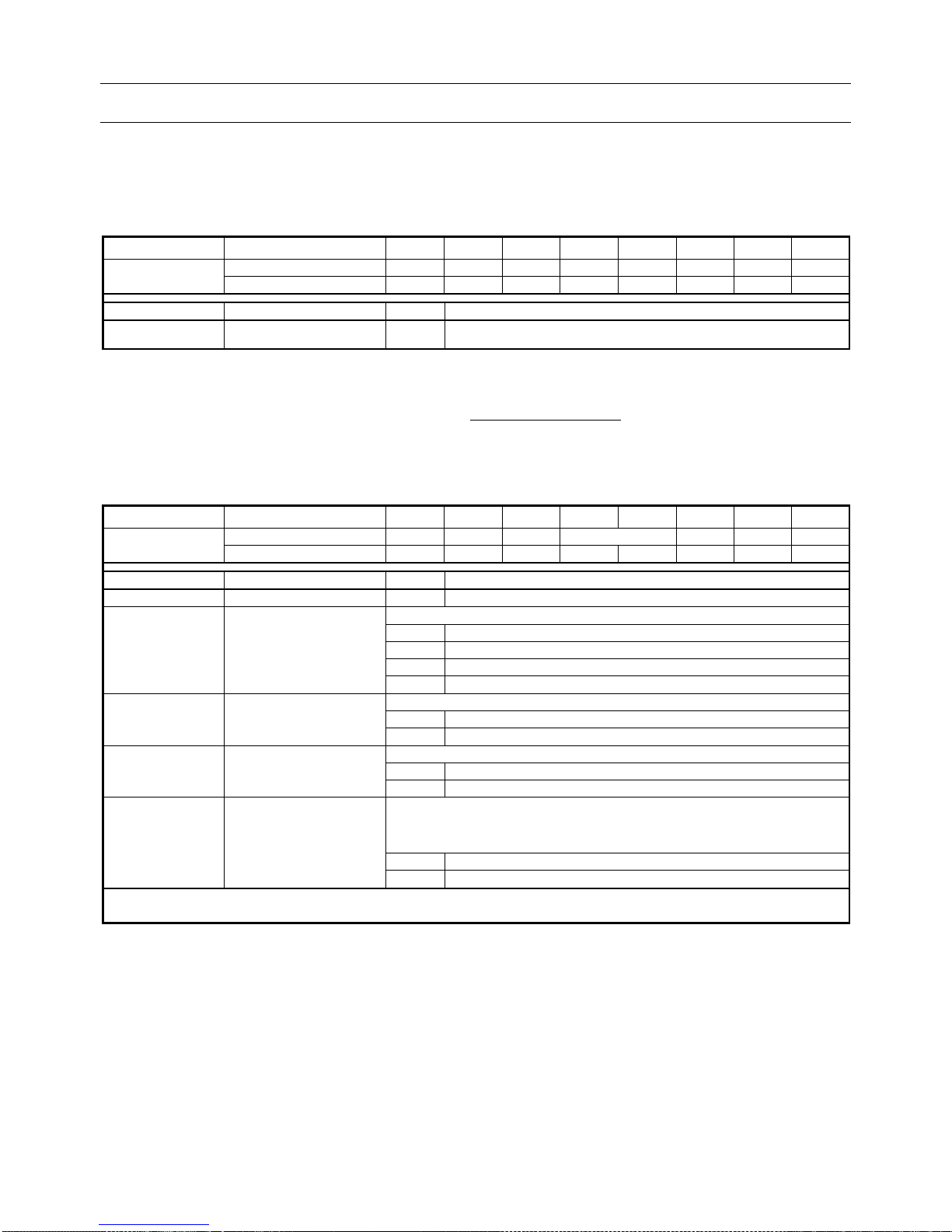
3. REGISTER ORGANIZATION
Registers are accessed by selecting a register address and then performing read or write operations. Multiple
reads or writes may be executed in a single access, with the address automatically incrementing after each byte.
18 registers (00h –11h) are available. The time registers are encoded in the Binary Coded Decimal format (BCD)
to simplify application use. Other registers are either bit-wise or standard binary format. When one of the RTC
registers is written or read, the contents of all time counters are frozen for up to 1 second. Therefore, faulty writing
or reading of the clock and calendar during a carry condition is prevented.
REGISTER OVERVIEW3.1.
After reset, all registers are set according to Table in section REGISTER RESET VALUES SUMMARY.
Address
Function
Bit 7
Bit 6
Bit 5
Bit 4
Bit 3
Bit 2
Bit 1
Bit 0
00h
Control1
TEST
SR
STOP
SR
CIE
12_24
CAP
01h
Control2
AIE
AF
MI
HMI
TF
FD
02h
Offset
MODE
OFFSET
03h
RAM
RAM data
04h
Seconds
OS
40
20
10
8
4
2
1
05h
Minutes
X
40
20
10
8
4
2
1
06h
Hours (24 hour)
X
X
20
10
8
4
2
1
Hours (12 hour)
AMPM
10
8
4
2
1
07h
Date
X
X
20
10
8
4
2
1
08h
Weekday
X
X
X
X
X
4
2
1
09h
Month
X
X
X
10
8
4
2
1
0Ah
Year
80
40
20
10
8
4
2
1
0Bh
Seconds Alarm
AE_S
40
20
10
8
4
2
1
0Ch
Minutes Alarm
AE_M
40
20
10
8
4
2
1
0Dh
Hours Alarm (24h)
AE_H
X
20
10
8
4
2
1
Hours Alarm (12h)
AMPM
10
8
4
2
1
0Eh
Date Alarm
AE_D
X
20
10
8
4
2
1
0Fh
Weekday Alarm
AE_W
X
X
X
X
4
2
1
10h
Timer Value
128
64
32
16
8
4
2
1
11h
Timer Mode
X
X
X
TD
TE
TIE
TI_TP
Bit positions labeled as X are not implemented and will return a 0 when read.

Micro Crystal
Ultra Small Real-Time Clock Module with I2C-Bus Interface RV-8263-C7
January 2019 11/61 Rev. 1.0
CONTROL REGISTERS3.2.
To ensure that all control registers will be set to their default values, the VDD level must be at zero volts at initial
power-up. If this is not possible, a reset must be initiated with the software reset command when power is stable.
Refer to section SOFTWARE RESET for details.
00h - Control1
Control and status register 1.
Address
Function
Bit 7
Bit 6
Bit 5
Bit 4
Bit 3
Bit 2
Bit 1
Bit 0
00h
Control1
TEST
SR
STOP
SR
CIE
12_24
CAP
Reset
0
0
0
0
0
0
0
0
Bit
Symbol
Value
Description
7
TEST
0
Normal mode.
1
External clock test mode. Do not use.
6
SR
Software Reset (see SOFTWARE RESET)
0
No software reset.
1
Initiate software reset; this bit always returns a 0 when read. For a software
reset, 01011000 (58h) must be sent to register Control1.
5
STOP
STOP bit (see STOP BIT FUNCTION)
0
RTC clock runs.
1
RTC clock is stopped; the upper part of the RTC divider chain flip-flops
(prescaler F2 to F14) are asynchronously set logic 0. The CLKOUT
frequencies 32.768 kHz, 16.384 kHz and 8.192 kHz are still available.
4:3
SR
Software Reset (see SOFTWARE RESET)
00
No software reset.
11
Initiate software reset; this bits always returns a 0 when read. For a
software reset, 01011000 (58h) must be sent to register Control1.
2
CIE
Compensation Interrupt Enable (see FREQUENCY OFFSET COMPENSATION)
0
No compensation interrupt will be generated.
1
Compensation interrupt pulses will be generated on pin INT
at every
compensation cycle.
1
12_24
12 or 24 hour mode (see TIME AND DATE REGISTERS and ALARM REGISTERS)
0
24 hour mode is selected (0 to 23).
1
12 hour mode is selected (1 to 12).
0
CAP
0
Must always be written with logic 0.

Micro Crystal
Ultra Small Real-Time Clock Module with I2C-Bus Interface RV-8263-C7
January 2019 12/61 Rev. 1.0
01h - Control2
Control and status register 2.
Address
Function
Bit 7
Bit 6
Bit 5
Bit 4
Bit 3
Bit 2
Bit 1
Bit 0
01h
Control2
AIE
AF
MI
HMI
TF
FD
Reset
0
0
0
0
0
0
0
0
Bit
Symbol
Value
Description
7
AIE
Alarm Interrupt Enable (see ALARM FUNCTION and INTERRUPT OUTPUT)
0
Disabled
1
Enabled
6
AF
Alarm Flag (see ALARM FUNCTION and INTERRUPT OUTPUT)
0
Read: Alarm Flag inactive
Write: Alarm Flag is cleared
1
Read: Alarm Flag active
Write: Alarm Flag remains unchanged
5
MI
Minute Interrupt Enable (see MINUTE AND HALF MINUTE INTERRUPT FUNCTION
and TIMER FLAG TF)
0
Disabled
1
Enabled
4
HMI
Half Minute Interrupt Enable (see MINUTE AND HALF MINUTE INTERRUPT
FUNCTION and TIMER FLAG TF)
0
Disabled
1
Enabled
3
TF
Timer Flag (see COUNTDOWN TIMER FUNCTION, INTERRUPT OUTPUT and
TIMER FLAG TF)
0
No timer interrupt generated
1
Flag set when timer interrupt generated
2:0
FD
000 to
111
CLKOUT Frequency (see CLKOUT FREQUENCY SELECTION)
FD
CLKOUT Frequency
000
32.768 kHz –Default value
001
16.384 kHz
010
8.192 kHz
011
4.096 kHz
100
2.048 kHz
101
1.024 kHz
110
1 Hz (1)
111
CLKOUT = LOW
(1) 1 Hz clock pulses are affected by compensation pulses (see FREQUENCY OFFSET COMPENSATION).

Micro Crystal
Ultra Small Real-Time Clock Module with I2C-Bus Interface RV-8263-C7
January 2019 13/61 Rev. 1.0
02h –Offset Register
This register holds the OFFSET value to digitally compensate the initial frequency deviation of the 32.768 kHz
oscillator or for aging adjustment (see FREQUENCY OFFSET COMPENSATION).
Address
Function
Bit 7
Bit 6
Bit 5
Bit 4
Bit 3
Bit 2
Bit 1
Bit 0
02h
Offset
MODE
OFFSET
Reset
0
0
0
0
0
0
0
0
Bit
Symbol
Value
Description
7
MODE
Offset Mode
0
Normal Mode: Offset is made once every two hours.
1
Fast Mode: Offset is made every 4 minutes.
6:0
OFFSET
-64 to
+63
Offset value.
For MODE = 0, each LSB introduces an offset of 4.34 ppm. For MODE = 1,
each LSB introduces an offset of 4.069 ppm. The values of 4.34 ppm and
4.069 ppm are based on a nominal 32.768 kHz clock. The offset value is
coded in two’s complement giving a range of +63 LSB to -64 LSB (see
FREQUENCY OFFSET COMPENSATION).
OFFSET
OFFSET compensation value
in decimal
Compensation pulses
in steps
CLKOUT frequency
offset in ppm(1)
Normal Mode
MODE = 0
Fast Mode
MODE = 1
0111111
63
+63
+273.420
+256.347
0111110
62
+62
+269.080
+252.278
:
:
:
:
:
0000001
1
+1
+4.340
+4.069
0000000
0
0
0
0
1111111
127
-1
-4.340
-4.069
1111110
126
-2
-8.680
-8.138
:
:
:
:
:
1000001
65
-63
-273.420
-256.347
1000000
64
-64
-277.760
-260.416
(1)The frequency offset measured at CLKOUT pin can be compensated by computing the compensation value OFFSET and writing it into
the Offset register (see OFFSET COMPENSATION CALCULATION WORKFLOW).
03h - RAM
Free RAM byte, which can be used for any purpose, for example, status byte of the system.
Address
Function
Bit 7
Bit 6
Bit 5
Bit 4
Bit 3
Bit 2
Bit 1
Bit 0
03h
RAM
RAM data
Reset
0
0
0
0
0
0
0
0
Bit
Symbol
Value
Description
7:0
RAM
00h to
FFh
User RAM

Micro Crystal
Ultra Small Real-Time Clock Module with I2C-Bus Interface RV-8263-C7
January 2019 14/61 Rev. 1.0
TIME AND DATE REGISTERS3.3.
04h - Seconds
This register holds the count of seconds, in two binary coded decimal (BCD) digits. Values will be from 00 to 59.
Address
Function
Bit 7
Bit 6
Bit 5
Bit 4
Bit 3
Bit 2
Bit 1
Bit 0
04h
Seconds
OS
40
20
10
8
4
2
1
Reset
1
0
0
0
0
0
0
0
Bit
Symbol
Value
Description
7
OS
Oscillator Stop (see OSCILLATOR STOP FLAG)
0
Clock integrity is guaranteed.
1
Clock integrity is not guaranteed; oscillator has stopped or has been
interrupted. –Default value
6:0
Seconds
00 to 59
Holds the count of seconds, coded in BCD format.
05h - Minutes
This register holds the count of minutes, in two binary coded decimal (BCD) digits. Values will be from 00 to 59.
Address
Function
Bit 7
Bit 6
Bit 5
Bit 4
Bit 3
Bit 2
Bit 1
Bit 0
05h
Minutes
X
40
20
10
8
4
2
1
Reset
0
0
0
0
0
0
0
0
Bit
Symbol
Value
Description
7
X
0
Unused
6:0
Minutes
00 to 59
Holds the count of minutes, coded in BCD format.
06h –Hours
This register holds the count of hours, in two binary coded decimal (BCD) digits. If the 12_24 bit is cleared (default)
(see CONTROL REGISTERS, 00h - Control1) the values will be from 0 to 23. If the 12_24 bit is set, the hour
values will range from 1 to 12 and the AMPM bit will be 0 for AM hours and 1 for PM hours.
Address
Function
Bit 7
Bit 6
Bit 5
Bit 4
Bit 3
Bit 2
Bit 1
Bit 0
06h
Hours (24 hour mode)
–default value
X
X
20
10
8
4
2
1
Hours (12 hour mode)
AMPM
10
8
4
2
1
Reset
0
0
0
0
0
0
0
0
Hours (24 hour mode), 12_24 = 0 –default value
Bit
Symbol
Value
Description
7:6
X
0
Unused
5:0
Hours (24 hour mode)
–default value
0 to 23
Holds the count of hours, coded in BCD format.
Hours (12 hour mode), 12_24 = 1
Bit
Symbol
Value
Description
7:6
X
0
Unused
5
AMPM
0
AM hours.
1
PM hours.
4:0
Hours (12 hour mode)
1 to 12
Holds the count of hours, coded in BCD format.

Micro Crystal
Ultra Small Real-Time Clock Module with I2C-Bus Interface RV-8263-C7
January 2019 15/61 Rev. 1.0
07h –Date
This register holds the current date of the month, in two binary coded decimal (BCD) digits. Values will range from
01 to 31. Leap years are correctly handled from 2000 to 2099.
Address
Function
Bit 7
Bit 6
Bit 5
Bit 4
Bit 3
Bit 2
Bit 1
Bit 0
07h
Date
X
X
20
10
8
4
2
1
Reset
0
0
0
0
0
0
0
1
Bit
Symbol
Value
Description
7:6
X
0
Unused
5:0
Date
01 to 31
Holds the current date of the month, coded in BCD format. –Default value
= 01
08h - Weekday
This register holds the current day of the week. Each value represents one weekday that is assigned by the user.
Values will range from 0 to 6.
Address
Function
Bit 7
Bit 6
Bit 5
Bit 4
Bit 3
Bit 2
Bit 1
Bit 0
08h
Weekday
X
X
X
X
X
4
2
1
Reset
0
0
0
0
0
1
1
0
Bit
Symbol
Value
Description
7:3
X
0
Unused
2:0
Weekday
0 to 6
Holds the weekday counter value.
Weekday
Bit 7
Bit 6
Bit 5
Bit 4
Bit 3
Bit 2
Bit 1
Bit 0
Weekday 1
0
0
0
0
0
0
0
0
Weekday 2
0
0
1
Weekday 3
0
1
0
Weekday 4
0
1
1
Weekday 5
1
0
0
Weekday 6
1
0
1
Weekday 7 –Default value
1
1
0

Micro Crystal
Ultra Small Real-Time Clock Module with I2C-Bus Interface RV-8263-C7
January 2019 16/61 Rev. 1.0
09h - Month
This register holds the current month, in two binary coded decimal (BCD) digits. Values will range from 01 to 12.
Address
Function
Bit 7
Bit 6
Bit 5
Bit 4
Bit 3
Bit 2
Bit 1
Bit 0
09h
Month
X
X
X
10
8
4
2
1
Reset
0
0
0
0
0
0
0
1
Bit
Symbol
Value
Description
7:5
X
0
Unused
4:0
Month
01 to 12
Holds the current month, coded in BCD format.
Month
Bit 7
Bit 6
Bit 5
Bit 4
Bit 3
Bit 2
Bit 1
Bit 0
January –Default value
0
0
0
0
0
0
0
1
February
0
0
0
1
0
March
0
0
0
1
1
April
0
0
1
0
0
May
0
0
1
0
1
June
0
0
1
1
0
July
0
0
1
1
1
August
0
1
0
0
0
September
0
1
0
0
1
October
1
0
0
0
0
November
1
0
0
0
1
December
1
0
0
1
0
0Ah - Year
This register holds the current year, in two binary coded decimal (BCD) digits. Values will range from 00 to 99.
Leap years are correctly handled from 2000 to 2099.
Address
Function
Bit 7
Bit 6
Bit 5
Bit 4
Bit 3
Bit 2
Bit 1
Bit 0
0Ah
Year
80
40
20
10
8
4
2
1
Reset
0
0
0
0
0
0
0
0
Bit
Symbol
Value
Description
7:0
Year
00 to 99
Holds the current year, coded in BCD format.

Micro Crystal
Ultra Small Real-Time Clock Module with I2C-Bus Interface RV-8263-C7
January 2019 17/61 Rev. 1.0
ALARM REGISTERS3.4.
0Bh –Seconds Alarm
This register holds the Seconds Alarm Enable bit AE_S and the alarm value for seconds, in two binary coded
decimal (BCD) digits. Values will range from 00 to 59.
Address
Function
Bit 7
Bit 6
Bit 5
Bit 4
Bit 3
Bit 2
Bit 1
Bit 0
0Bh
Seconds Alarm
AE_S
40
20
10
8
4
2
1
Reset
1
0
0
0
0
0
0
0
Bit
Symbol
Value
Description
7
AE_S
Seconds Alarm Enable bit (see ALARM FUNCTION)
0
Enabled
1
Disabled –Default value
6:0
Seconds Alarm
00 to 59
Holds the alarm value for seconds, coded in BCD format.
0Ch –Minutes Alarm
This register holds the Minutes Alarm Enable bit AE_M and the alarm value for minutes, in two binary coded
decimal (BCD) digits. Values will range from 00 to 59.
Address
Function
Bit 7
Bit 6
Bit 5
Bit 4
Bit 3
Bit 2
Bit 1
Bit 0
0Ch
Minutes Alarm
AE_M
40
20
10
8
4
2
1
Reset
1
0
0
0
0
0
0
0
Bit
Symbol
Value
Description
7
AE_M
Minutes Alarm Enable bit (see ALARM FUNCTION)
0
Enabled
1
Disabled –Default value
6:0
Minutes Alarm
00 to 59
Holds the alarm value for minutes, coded in BCD format.

Micro Crystal
Ultra Small Real-Time Clock Module with I2C-Bus Interface RV-8263-C7
January 2019 18/61 Rev. 1.0
0Dh –Hours Alarm
This register holds the Hours Alarm Enable bit AE_H and the alarm value for hours, in two binary coded decimal
(BCD) digits. If the 12_24 bit is cleared (default value) (see CONTROL REGISTERS, 00h - Control1) the values will
range from 00 to 23. If the 12_24 bit is set, the hour values will be from 01 to 12 and the AMPM bit will be 0 for AM
hours and 1 for PM hours.
Address
Function
Bit 7
Bit 6
Bit 5
Bit 4
Bit 3
Bit 2
Bit 1
Bit 0
0Dh
Hours Alarm (24 hour
mode) –default value
AE_H
X
20
10
8
4
2
1
Hours Alarm (12 hour
mode)
AMPM
10
8
4
2
1
Reset
1
0
0
0
0
0
0
0
Hours Alarm (24 hour mode), 12_24 = 0 –default value
Bit
Symbol
Value
Description
7
AE_H
Hours Alarm Enable bit (see ALARM FUNCTION)
0
Enabled
1
Disabled –Default value
6
X
0
Unused
5:0
Hours Alarm (24 hour
mode) –default value
00 to 23
Holds the alarm value for hours, coded in BCD format.
Hours Alarm (12 hour mode), 12_24 = 1
Bit
Symbol
Value
Description
7
AE_H
Hours Alarm Enable bit (see ALARM FUNCTION)
0
Enabled
1
Disabled –Default value
6
X
0
Unused
5
AMPM
0
AM hours.
1
PM hours.
4:0
Hours Alarm (12 hour
mode)
01 to 12
Holds the alarm value for hours, coded in BCD format.

Micro Crystal
Ultra Small Real-Time Clock Module with I2C-Bus Interface RV-8263-C7
January 2019 19/61 Rev. 1.0
0Eh –Date Alarm
This register holds the Date Alarm Enable bit AE_D and the alarm value for the date, in two binary coded decimal
(BCD) digits. Values will range from 01 to 31.
Address
Function
Bit 7
Bit 6
Bit 5
Bit 4
Bit 3
Bit 2
Bit 1
Bit 0
0Eh
Date Alarm
AE_D
X
20
10
8
4
2
1
Reset
1
0
0
0
0
0
0
0
Bit
Symbol
Value
Description
7
AE_D
Date Alarm Enable bit (see ALARM FUNCTION)
0
Enabled
1
Disabled –Default value
6
X
0
Unused
5:0
Date Alarm
01 to 31
Holds the alarm value for the date, coded in BCD format.
0Fh –Weekday Alarm
This register holds the Weekday Alarm Enable bit AE_W and the alarm value for the weekday, in two binary coded
decimal (BCD) digits. Values will range from 0 to 6.
Address
Function
Bit 7
Bit 6
Bit 5
Bit 4
Bit 3
Bit 2
Bit 1
Bit 0
0Fh
Weekday Alarm
AE_W
X
X
X
X
4
2
1
Reset
1
0
0
0
0
0
0
0
Bit
Symbol
Value
Description
7
AE_W
Weekday Alarm Enable bit (see ALARM FUNCTION)
0
Enabled
1
Disabled –Default value
6:3
X
0
Unused
2:0
Weekday Alarm
0 to 6
Holds the weekday alarm value, coded in BCD format.
Micro Crystal
Ultra Small Real-Time Clock Module with I2C-Bus Interface RV-8263-C7
January 2019 20/61 Rev. 1.0
TIMER REGISTERS3.5.
10h –Timer Value
This register holds the current value of the Countdown Timer. It may be loaded with the desired starting value when
the Countdown Timer is stopped.
Address
Function
Bit 7
Bit 6
Bit 5
Bit 4
Bit 3
Bit 2
Bit 1
Bit 0
10h
Timer Value
128
64
32
16
8
4
2
1
Reset
0
0
0
0
0
0
0
0
Bit
Symbol
Value
Description
7:0
Timer Value
00h to
FFh
Countdown Timer Value (see COUNTDOWN TIMER FUNCTION)
Countdown Period in seconds:
Countdown Period = Timer Value
Timer Clock Frequency
11h –Timer Mode
This register controls the Countdown Timer function.
Address
Function
Bit 7
Bit 6
Bit 5
Bit 4
Bit 3
Bit 2
Bit 1
Bit 0
11h
Timer Mode
X
X
X
TD
TE
TIE
TI_TP
Reset
0
0
0
1
1
0
0
0
Bit
Symbol
Value
Description
7:5
X
0
Unused
4:3
TD
Timer Clock Frequency (see COUNTDOWN TIMER FUNCTION)(1)
00
4.096 kHz
01
64 Hz(2)
10
1 Hz(2)
11
1/60 Hz –Default value(2)
2
TE
Timer Enable
0
Disabled –Default value
1
Enabled
1
TIE
Timer Interrupt Enable
0
No interrupt generated from timer. –Default value
1
Interrupt generated from timer.
0
TI_TP
Timer Interrupt Mode.
How the setting of TI_TP and the Timer Flag TF can affect the INT
pulse generation is
explained in sections COUNTDOWN TIMER FUNCTION and MINUTE AND HALF
MINUTE INTERRUPT FUNCTION.
0
Interval Mode. Interrupt follows Timer Flag TF. –Default value
1
Pulse Mode. Interrupt generates a pulse.
(1) When not in use, the TD field is recommended to be set to 11 (1⁄60 Hz) for power saving.
(2) Time periods can be affected by compensation pulses (64 Hz only in MODE = 1), (see FREQUENCY OFFSET COMPENSATION).
Table of contents
Other Micro crystal Control Unit manuals

Popular Control Unit manuals by other brands


Wecon
Wecon LX3V-2TC2DAI-BD user manual

IBM
IBM BladeCenter Advanced Management Module installation guide

Watts
Watts 007 Series INSTRUCTION, INSTALLATION, MAINTENANCE AND REPAIR MANUAL

ICP DAS USA
ICP DAS USA tSH-735 quick start

Air Torque
Air Torque PT Series INSTALLATION, MAINTENANCE AND OPERATING INSTRUCTION

Lutron Electronics
Lutron Electronics GRAFIK Eye QSGRN-6PCE Installation and operation guide


