MICROBEE Premium Plus + Instructions for use
Page 1 of 31. Version 1.03 September 2012 Microbee Premium Plus+ | Construction Manual
Premium
PLUS +
Construction Manual
Microbee Technology Pty Ltd
P.O. Box 709
Lilydale, Victoria
3140

Page 2 of 31. Version 1.03 September 2012 Microbee Premium Plus+ | Construction Manual
Premium Plus+
Construction Manual
Table of Contents
1. Introduction / Requirements ...................................... 3
2. Getting tarted - Preparing the Baseboard PCB ........... 3
3. Passive components ................................................... 5
4. Keyboard Frame & Key switch assembly ....................... 8
5. I.C. sockets and PCG ram adapter PCB ........................ 14
6. Integrated Circuits ..................................................... 15
7. Core board ockets .................................................... 16
8. Completing the Base Board .......................................... 17
9. Final checks & first power up...................................... 19
10. Bill of materials ...........................................................22
11. ‘Check photos’ ...........................................................25

Page 3 of 31. Version 1.03 September 2012 Microbee Premium Plus+ | Construction Manual
1.a Introduction
Firstly, Congratulations on urchasing your new Limited Edition Microbee Premium Plus + kit
com uter! Whether you have never had a Microbee before, or have been a Microbee fan for
a very long time, we ho e that you enjoy the ex erience of building your own unit and
getting it to do things for you.
As mentioned above, the Premium Plus is a limited edition release with only 105 units being
made available in total. Although we will be designing other Microbee kits in the future, we
will not be re- roducing the Premium case, so 105 units is the maximum number of
Premium Plus machines that we can su ly. So, to state the obvious, not only do you have
a great kit to assemble & use, but you have a collector’s item as well.
1.b Requirements
Before you get started on the construction of your new Microbee, there are a number of
things that you need to do:
•Read this construction manual com letely to see whether you have the knowledge
and skills to com lete the assembly & testing of the unit. It is im ortant to note that
once construction has started, the kit cannot be returned for a refund should you
decide that the task is beyond you.
•Check off all of the com onents against the arts list included at the end of this
manual – if anything is missing from the kit, lease contact Microbee Technology via
our website (www.microbeetechnology.com.au) and let us know.
•You will need the following items to construct this kit :
A soldering iron with a good quality ti
Good to very good soldering skills
The ability to identify com onents & their values (color codes etc..)
Resin cored Solder (there is none su lied with the kit)
A air of electronics grade side-cutters that facilitate close cutting (ie leaving
very little com onent leg left at the joint). This is articularly im ortant when
assembling the key switch ada ter PCBs.
A Phili s head screw driver
A shar hobby knife
A small air of liers
A basic multimeter (measuring DC Volts, and resistance)
Care & Patience!
Provided you follow the instructions in this manual and take time & care in doing so, you
should have a working Microbee very soon.
2.a Getting tarted
The first thing to do is to set u a suitable works ace where you will be able to lay all the
com onents out and have room to assemble, solder and test.

Page 4 of 31. Version 1.03 September 2012 Microbee Premium Plus+ | Construction Manual
If you have not done so already, lease take the time to check through the com onent list &
check off each item to make sure you have everything that you need that is su osed to be
su lied with the kit. We do check every kit for com leteness, but mistakes can ha en, so
its better that you make sure that it is com lete before you start construction.
2.b Preparing the Baseboard PCB
You should have a blank Printed Circuit board labelled 8501-4-0CR (this can be found on the
PCB on the com onent side, rear, right side, near the 5 Pin DIN socket osition).
The PCB has a number of configuration ‘jum ers’ on it where the default osition is made by
tracks connecting 2 vias (a ‘via’ is a small lated hole in the board that connects to side
tracks to bottom side tracks).
Three of these jum ers have to be cut from their default osition and left ‘o en’. These are
Jum er W1 osition 3 A-B, Jum er W4 1-2 and Jum er W2 1-2 See the diagrams below :
W1 Pos 3 A-B
W4 1-2
W2 1-2
Be very careful when you are making the cuts not to sli and cut another track. It is more
controlled just to ‘take a little divot’ out of the track between the 2 vias, using the shar
< Before
< After

Page 5 of 31. Version 1.03 September 2012 Microbee Premium Plus+ | Construction Manual
hobby knife in a twisting / digging way rather than trying to slice through the track. Now we
are ready to start lacing the com onents onto the board.
3. Passive components
We shall start lacing com onents by starting with the ca acitors. There are only 5 different
ty es / values of ca acitor on the board and they are as follows :
61 x 100nF by ass ca (su lied on a ta e)
7 x 4.7uF 16v Tag Tantalum ca [Polarised], 2 x 4.7uF 25v Tag Tantalum ca [Polarised]
1 x 10nF ca (single, on ta e)
1 x 47 F ca (single, on ta e)
1 x 470uF 25v Electrolytic ca [Polarised]
You can do these in any order, but take care with the olarised com onents that you insert
them so that the ‘+’ marking on the com onent is on the same in side as the ‘+’ marking
on the white com onent legend on the PCB. If these are inserted the wrong way around,
they can ex lode when ower is a lied.
Please refer to the ‘stuffing diagram’ below showing where each ca acitor is to be laced.
With the com onents su lied on ta e, it is easier to cut the legs of the com onents at the
edge of the ta e rather than try to remove (unstick) them from the ta e. This still leaves
enough com onent leg left to effectively solder them into the PCB and trim them once done.
Page 6 of 31. Version 1.03 September 2012 Microbee Premium Plus+ | Construction Manual
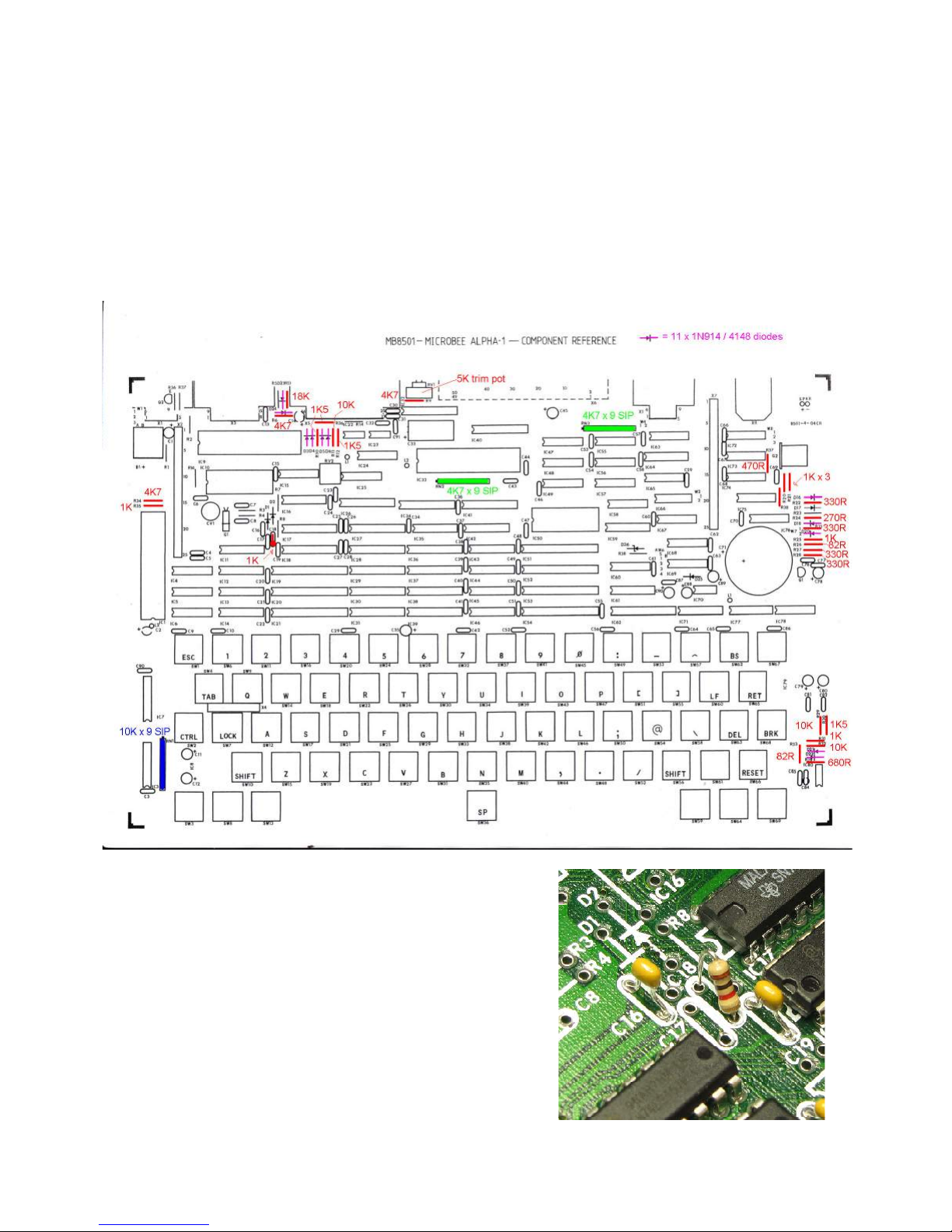
Next we shall lace all of the resistors and also the small signal diodes.
Referencing the marked u com onent overlay below, work through the resistors section of
the arts list which gives values & com onent reference designators, ticking off each
com onent as you go. The resistor SIPs (Single Inline Package) are 9 resistors in one
ackage with all of those resistors connected to a common in. If you have a look at the
SIP, the value is written on one side (472 = 4.7K, 103 = 10K) and the dot at the left end
signifies in 1. Make sure you line u in 1 with the marking on the PCB.
Mounting the 11 x 1N914 / 4148 diodes is straight forward but make sure the band on the
body of the diode matches the olarity shown on the com onent legend.
Note also that one of the resistors gets mounted
at osition ‘C18’. The Premium was originally
designed to have an LM386 integrated am lifier
as its s eaker driver and C18 was art of the
cou ling into the am lifier, however, the LM386
am was very noisy – even when there was no
sound being out ut from the Microbee, so the
LM386 circuit was re laced by a basic one-
transistor s eaker driver like the original
Microbees had. A 1K resistor gets mounted
vertically in the C18 osition as art of this
circuit. See the hoto o osite.

Page 7 of 31. Version 1.03 September 2012 Microbee Premium Plus+ | Construction Manual
The s eaker volume control (RV1)
is a 5K ohm trim ot which gets
mounted on the under side of the
PCB and soldered on the to side.
See the hoto o osite which
shows the PCB u side down with
the trim ot facing the edge of the
board.
At this oint there are just the 2 transistors & 1 crystal to mount on the board.
Transistor Q1 is mounted on the PCB just as the com onent legend shows. The middle leg
(the BASE) will need to be bent out a little to fit into the PCB.
The 13.5Mhz crystal lays flat
(horizontal) on the PCB and needs
to be located a little bit backward
from the hole in the PCB for the
case ost.
This means that the com onent
legs have to be lead-formed with
an offset as in the icture to the
right.
The s eaker driver transistor (a BC548) gets
located at what was the LM386 location – IC23.
As you can see from the hoto o osite, the
Emitter & Collector of the transistor go into ins 5
& 6 of the IC location, and the BASE lead gets
bent backwards & is soldered into IC23 – in 3.
Note that the round side of the transistor is facing
toward the edge of the PCB.
Also, a LINK is needed between the + & -
terminals at the C33 com onent location as
shown in the same hoto.
LINK
Having installed all of the assive com onents now, there are a few IC’s to insert before we
can start mounting the keyboard frame & regulators. IC3 (a 74HC151) and IC7 (a 74LS156)
form art of the keyboard scanning circuit & are located in the area that the keyboard frame
covers once assembled, so it is a good idea to solder these in now. Likewise, IC80 (a
CA3140 o am ) on the right side of the board, should be soldered into lace now.
Connectors at the rear of the board can be soldered in at this oint. Once the keyboard
frame is in lace (in the next few ste s) the board will need to be owered u to check the
o eration of the 2 regulators, so having (at least) the ower connector fitted will be
essential. After the connectors are installed, you can refer to ‘check hoto 6’ at the end of
the manual and the board being assembled should look the same as the hoto.
Page 8 of 31. Version 1.03 September 2012 Microbee Premium Plus+ | Construction Manual
4. Keyboard Frame & key switch assembly
The Microbee Premium Plus keyboard is made u of a number of arts which includes
individual mechanical key switches, key to s (ca s), a metal keyboard frame and key switch
ada ter PCBs. In lanning and designing the Premium Plus, large efforts were made to try
and rocure key switches that were the same hysical form as the original ones. There was
no exact match to be found. Some came close (like the Cherry brand MX series) but were
cost rohibitive, others had non-suitable shaft styles and so on. All of the key switches that
we looked at also had different in s acings & locations as well. While we could have
scra ed the existing stock of Premium series baseboards and made new ones to suit a
different style of switch, this was deemed to be wasteful & ex ensive. Seen as the Premium
Plus is a limited edition kit, the best solution was to rovide a small ada ter PCB for each of
the new key switches, so that the assembled switch would then suit the original PCBs. This
also made the solution suitable for eo le who want to re lace the keyboard in other
Microbee models.
4.a Key switch assembly
Assembly of all of the key switch ada ters & fitting them to the key switches takes quite an
amount of time. You can ex ect to s end 2 hours working through the whole lot of keys, so
have some atience & take a break when you need to because it is better to s end as much
time as it needs to do a great job rather than rushing it through. If done well, you will have
a decent keyboard for your Microbee that will last well. If you rush in assembling them, it is
likely that you will have keys that don’t work as well as they should.
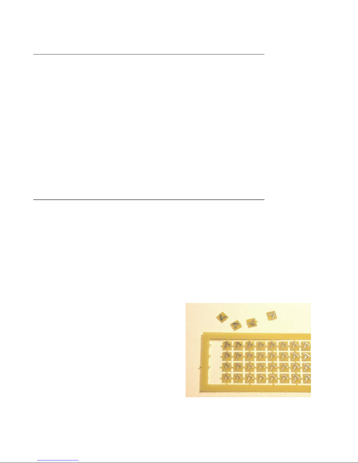
In your kit, you will have a bag s ecifically of keyboard bits. This includes the key to s, key
switches, gold PCB ins, mounting hardware and so on. There is also a PCB su lied that
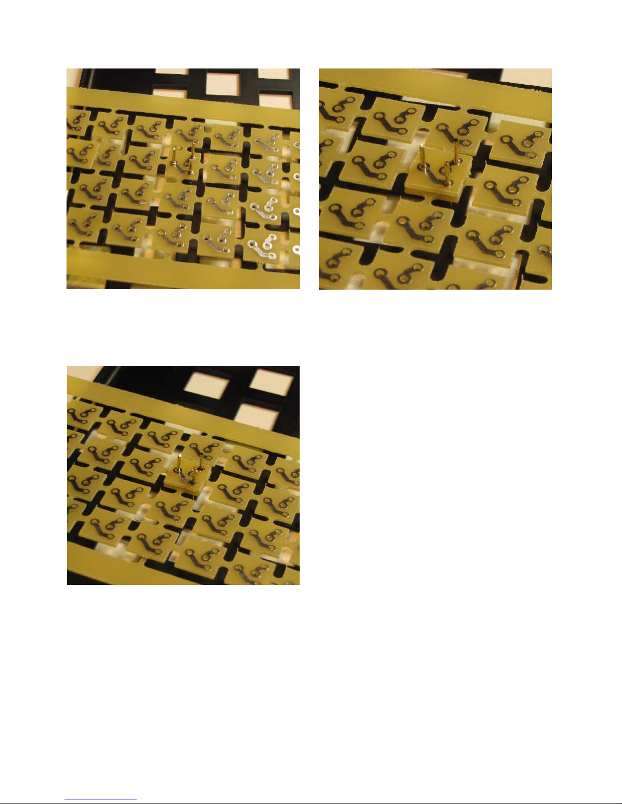
has 68 (64 needed, lus 4 s are) key switch ada ter PCBs in a frame.
All of the individual ada ter PCB’s are held
together in the frame with breakout tabs.
That is, on the edges of each PCB there is a
little bit of PCB material that connects one
PCB to another to hold all of them in the
frame while the board is being manufactured.
At these oints there are very small holes
which rovide a breaking oint. If this oint
is flexed, it will break a art & each individual
PCB will come away from the others. Refer to
the hoto to the right which shows some of
the key switch ada ter PCBs broken out from
the frame.
Page 9 of 31. Version 1.03 September 2012 Microbee Premium Plus+ | Construction Manual
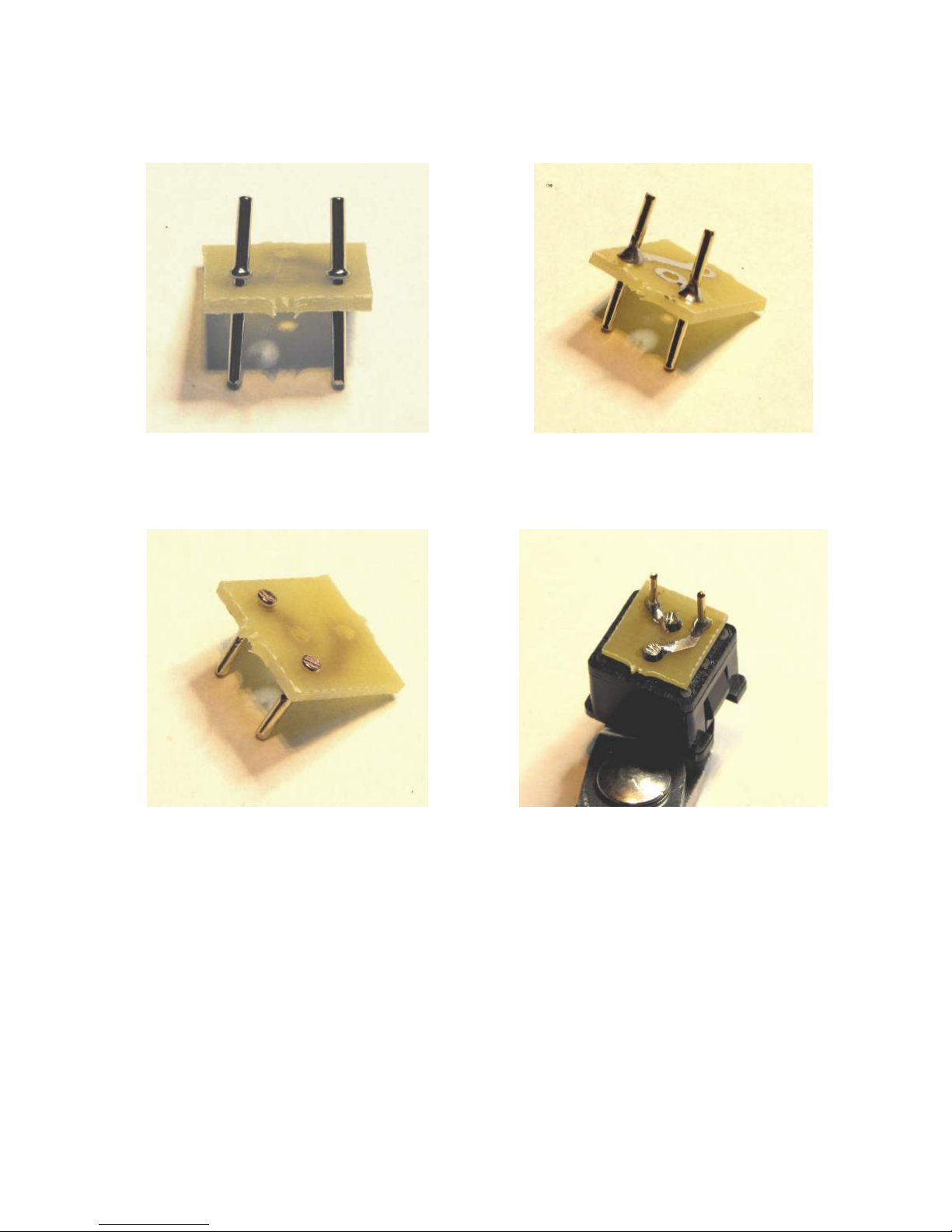
The following shows the general rocedure for making u and fitting the key switch ada ter
PCBs to the key switches.
1. Insert the PCB ins from the non-track
side of the PCB, with the longer section of
the in through the hole.
2. Solder the 2 PCB ins in lace with a nice
triangular fillet or even slightly concave.
3. Trim the excess in length as close as
ossible without removing the collar (this
locks the in into the PCB and sto s it from
falling out when the in is soldered into the
main PCB later
4. Solder the finished ada ter onto the back
of a key switch. Make sure that the ada ter
is flat against the back surface of the key
switch. This is im ortant as we do not want
any ‘slack’ or chance of ressure on the ins
of the switch. If the ins of the switch get
ushed into the body, the switch will not
work ro erly.
Note that in ste 4, the ada ter PCB will be at a slight angle if correctly installed as the
collars on the PCB ins will kee it from sitting absolutely flush. This is o.k.
The whole rocedure is quite fiddly and it is tricky to ensure that the ins are u right and
arallel to each other (and hence kee ing the same s acing). The following hotos (on the
next age) show a setu that makes the job easier & more accurate.
Page 10 of 31. Version 1.03 September 2012 Microbee Premium Plus+ | Construction Manual
1. With the PCB ada ter board s read across
the u -turned keyboard frame, insert 3 PCB
ins (short end through the holes)
2. Place a ‘broken-out’ ada ter on to so that
it is then sitting on the collars of the PCB
ins (using 3 ins kee s the ada ter PCB
level)
3. Solder the 2 required ins, leaving the 3rd
un-soldered, and then remove the ada ter &
trim the ins as described earlier.
Obviously, as you do more and more of the
ada ters, the PCB frame will have less and
less ada ters in it and the last few will
robably have to be done with no su ort
from the frame.
One other ti is that if you line the ada ter
that you are working on u over a key switch
hole in the keyboard frame below it, you can
ress down on the centre of the ada ter so
that it ensures that all of the PCB ins are
ressed ‘u ’ against the bottom of the
ada ter as you solder it. This also aids in
making sure the ins are straight & arallel.
There is a bit of a ‘knack’ to doing this, but
after doing a few, you should see it get
easier.
Remember that only 64 key switches are
needed, so the last 4 ada ters in the frame
do not need to be assembled.
Page 11 of 31. Version 1.03 September 2012 Microbee Premium Plus+ | Construction Manual
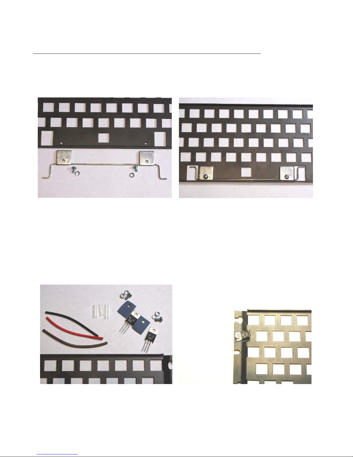
4.b Keyboard frame assembly & mounting
Lay the keyboard frame flat on your work surface with the to side facing down.
The torsion bar for the s ace bar key has to be installed before the keyboard frame is in
lace on the PCB, otherwise it is very difficult to install.
This icture shows the arts required – the
torsion bar, 2 clam s & bolts with s ring
washers.
The torsion bar is now in lace held into the
corner of the keyboard frame by the clam s
which are bolted into threaded holes in the
keyboard frame.
Mounting the 2 x 7805 5volt regulators is next. Both regulators bolt directly to the keyboard
frame underside with a thermal transfer silicon-rubber ad. The regulator for the right hand
side [eventually] gets soldered directly to the main PCB. The regulator on the left hand side
of keyboard however requires short wires to be attached which then get soldered into the
main PCB. This is due to the lack of s ace on that side of the keyboard frame (having art
of the keyboard scanning circuit on the main PCB at that oint).
The arts required – 2 x 7805’s, thermal
washers, nuts, bolts, s ring washers, wire
and heat shrink tubing.
The right hand side regulator (it’s on the
left of the keyboard frame in this ‘u side
down’ view) gets mounted at a slight angle
with its legs bent u at right angles.

Page 12 of 31. Version 1.03 September 2012 Microbee Premium Plus+ | Construction Manual
When fitting u this regulator, bolt it down but do not tighten the bolts too much. At this
stage we want the regulator to be held firmly in lace, but to be able to adjust the osition
of it and get the right angle to allow the legs to meet with the holes in the main PCB where
it is to be soldered in. This will take a bit of fiddling to get everything to line u .
It is advisable at this oint to sit the main PCB in the bottom half or the case so that you can
osition the keyboard frame correctly over the main PCB while taking into account the
mounting osition of the keyboard frame into the case bottom. Once you have the regulator
set u to that the ins line u with the holes in the PCB, you can tighten the bolts to kee it
that way. Do NOT solder the regulator to the PCB at this time.
The left hand side regulator…
Trim the legs back to just near the wider
art of the leg. Also, re are 3 wires about
30mm long and tin the ends.
Mount the regulator with the thermal ad,
nut, bolt & s ring washer as shown. Solder
the wires on & slide the heat shrink tubing
onto each so that the joints are insulated
from each other. The ti of the soldering
iron will shrink the tubing.
Next, the wires that you have just soldered
to the regulators’ ins need to be bent u
as shown in the hoto.
These wires will connect the regulator to
the main PCB – they are essentially
extending the legs of the regulator so that
they reach the correct osition and can be
soldered in.
You may need to trim the width of each
wire a little so as to be able to fit the ends
of the wires through the holes in the PCB in
the ads for the regulator osition.
Page 13 of 31. Version 1.03 September 2012 Microbee Premium Plus+ | Construction Manual
Soldering the regulators into the main PCB..
Ensure that the wires attached to the
regulator fit through the ad holes & then
solder all three into the main PCB.
As shown in the hoto to the left, the wires
line u in order with no need to cross any
over.
This is the same as having the regulator
ins bent at right angles toward the PCB &
soldered in.
Now, before the other regulator gets soldered into lace, the ositioning and height of the
keyboard frame (with res ect to the main PCB) needs to be correct.
It is at this oint that some key switches are needed to be laced into the frame.
To start with, just 5 keys are needed – in the ‘outer most’ ositions on the keyboard where
the ‘ESC’, ‘Backs ace’, ‘U Arrow’ and ‘Right Arrow’ keys are found. The ‘S ace bar’ osition
is also used. Once again, it is easier to align the osition of the keys if the main PCB and
the keyboard frame is sitting in their correct ositions in the base of the case.
Inserting the key switches into the frame will require a reasonable amount of force as they
are a tight fit. Watch to see that the PCB ins on the ada ter of each key switch go through
the holes in the main PCB as they should. Once the 5 key switches are in the frame,
carefully lift the frame & main PCB out of the bottom of the case, ensuring that it all stays
together and then ‘tack’ solder 1 in of each key switch. This is a bit of a juggling act but
can be achieved by holding the PCB and frame on one side, while soldering the ins.
Do not a ly too much heat to the ins while soldering them as this will melt the solder
that holds the ins in lace in the ada ter.
Once the five key switches have been ‘tacked’ in lace, the keyboard frame can be checked
to see if it is ositioned well and that the height from the PCB to the keyboard frame is the
same on all sides. Ty ically, the PCB ins of each key switch should rotrude through the
PCB by around 2mm. Once the keyboard frame is all level, the right hand side regulator can
be soldered into the main PCB.
Initial test
Now that the regulators are soldered into lace, it is a good idea to check to see if there are
any shorts & whether the two 5 volt ower rails on the main PCB work as required. If
something is not right at this oint it is easier to get to the regulators than when the full
keyboard is assembled.
First check that there are no short circuits.
With a multimeter set to low ohms range, check the following oints on the PCB:
a) across the main in ut ca acitor (C71) – you should see an initial low ohms reading
due to the charging of the ca acitor (by the multimeter), but after a small amount of
time, this should be a large resistance value. As long as it is not ermanently below
10 ohms, then all is well.
Page 14 of 31. Version 1.03 September 2012 Microbee Premium Plus+ | Construction Manual
b) across IC16 ins 8 & 16 – this should be a fairly large resistance value and re resents
the out ut side of one of the 5volt regulators. Once again, as long as it is not
ermanently below 10 ohms, then all is well.
c) across IC72 ins 7 & 14 – this should be a fairly large resistance value and re resents
the out ut side of the other 5volt regulator. Once again, as long as it is not
ermanently below 10 ohms, then all is well.
If you find any shorts in the above ste s, check over your soldering work – articularly at
each regulator and correct these before moving on to the next ste s.
Power on test
The Microbee Premium Plus runs with an in ut ower su ly of 10 – 14 volts DC which is fed
into the main board via the 5 in DIN connector. 10 Volts is referred as the regulators will
run cooler.
With the multimeter set to measure D.C. volts and a suitable range selected to measure the
10 – 14 Volts D.C., a ly ower and quickly measure the in ut voltage across C71 to
confirm that the ower su ly is getting to the board o.k.
Measure the two 5 volts rails at:
a) IC16 – negative meter lead to in 8, ositive to in 16 – should read +5.0v +/- 10%
b) IC72 – negative meter lead to in 7, ositive to in 14 – should read +5.0v +/- 10%
If these are measured o.k. then construction can continue and the un-soldered ins on the 5
key switches can now be soldered.
5. I.C. sockets & PCG ram adapter PCB
Sockets have been su lied in the kit for the larger logic devices including the CPU, PIO,
6545, the Font ROM, the Screen RAMs and the Gold PAL. These can be soldered onto the
PCB now.
There are 3 x 40 in sockets for locations IC1, IC9 & IC33.
There are 3 x 24 in (skinny) sockets for locations IC19, 20 & 21. Note that these locations
are actually for 28 in arts and the 24 in sockets get soldered into the PCB so that in 1 of
each socket gets soldered into the in 3 location on the board – i.e. the left-most 4 ads
( ins 1,2, 27 & 28) are left em ty.
There is 1 x 24 in (skinny) socket for location IC62.
There is 1 x 24 in (normal width) socket for location IC50.
The original Microbee Premium Series
com uters were su lied as standard with
16k bytes of Programmable Character
Generator (PCG) memory. The Premium
baseboard was designed for a maximum of
32K bytes of PCG memory however and the
Premium Plus kit includes this as standard.
To im lement the full 32k, we have
designed a small ada ter PCB that takes a
single 32k x 8 bit static ram rather than the
4 individual 8k x 8 bit static RAMs in the
original design. The ada ter is re-made
and has to be soldered into the baseboard.
The PCG ram ada ter board fits onto the
baseboard at IC locations IC53/4 and IC61.

Page 15 of 31. Version 1.03 September 2012 Microbee Premium Plus+ | Construction Manual
The ins of the PCG ram ada ter PCB do not quite rotrude through the other side of the
baseboard PCB, however, there is enough of the in in the ad holes that they can still be
soldered by ‘flooding’ the hole with solder. A ly just enough solder for it to ‘wick’ down the
hole and surround the in so as to get a good solder joint.
6. Integrated Circuits.
Now it is time to start installing the integrated circuits.
Start with all of the smaller 14 & 16 in devices. Take care that each is located at the correct
IC location. Check as you go that the correct device for that location is being installed by
cross referencing the arts list. The ICs are su lied on a sheet of anti-static foam with a
com onent reference overlay on it.
* Handy Ti * When installing all of the ICs, solder just 2 diagonal ins to start with. For
exam le, on a 14 in device, solder in 7 & in 14 to the board & leave the rest for now.
Then, once all ICs are in osition and verified for correct ty e & orientation, solder the rest
of the ins for each device. This way, if you make a mistake and (say) ut a device at the
wrong location, it is easy to remove the device and make the correction.
While it is ossible to use IC sockets for all of the devices, it is not recommended as, over
time, socket contacts oxidise and the circuit erformance can be degraded.
Next, move onto the larger 20 in devices. Install these in the same manor, checking that
the location and device ty es are correct, along with making sure of the ro er orientation.
It is a good idea at this oint to do a thorough visual ins ection of your soldering and check
for any com onent leads that may be shorting. As quite a few of the ICs are close together,
it is common for the legs of adjacent com onents to touch each other on the under side of
the board. Trim any leads that are close to each other to ensure no shorts can occur.
Page 16 of 31. Version 1.03 September 2012 Microbee Premium Plus+ | Construction Manual
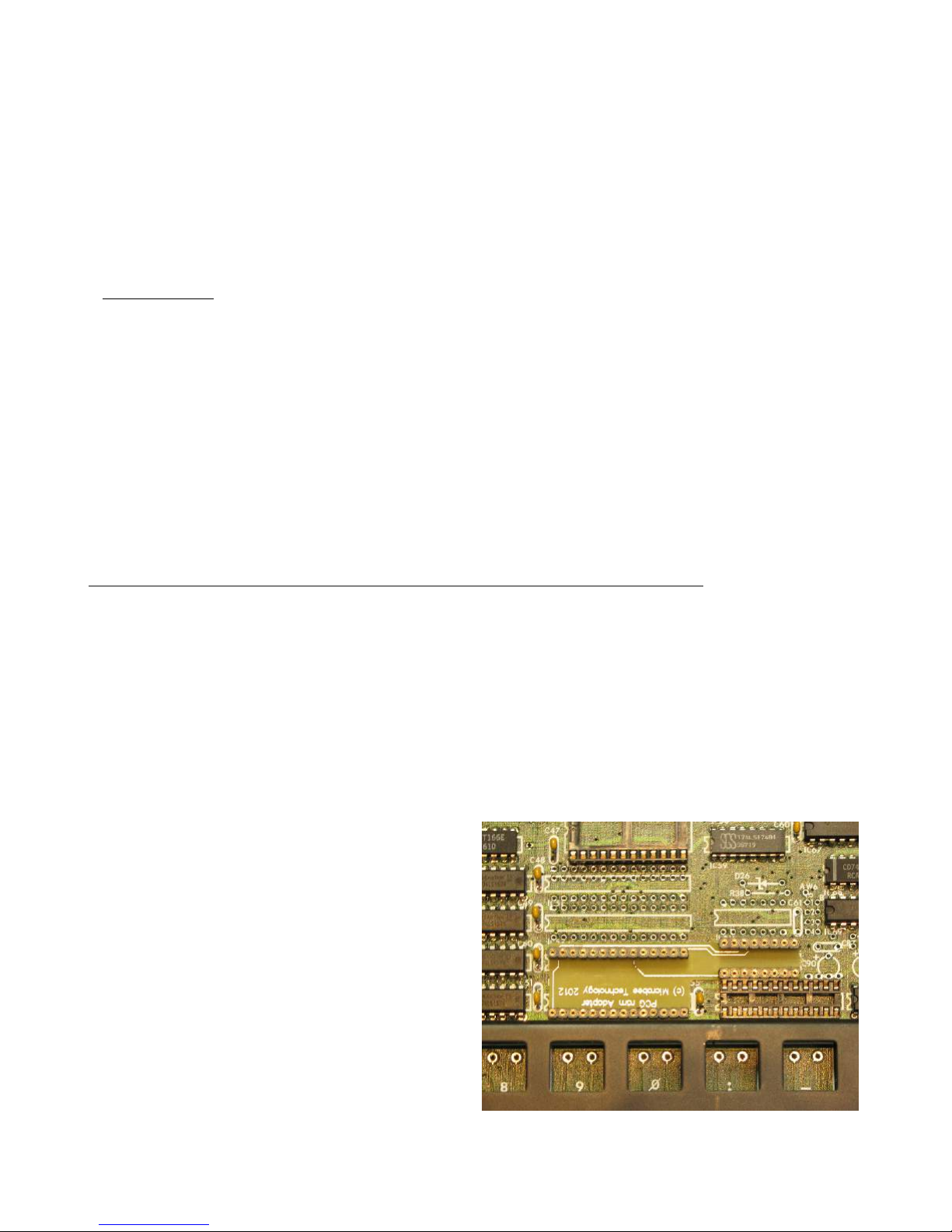
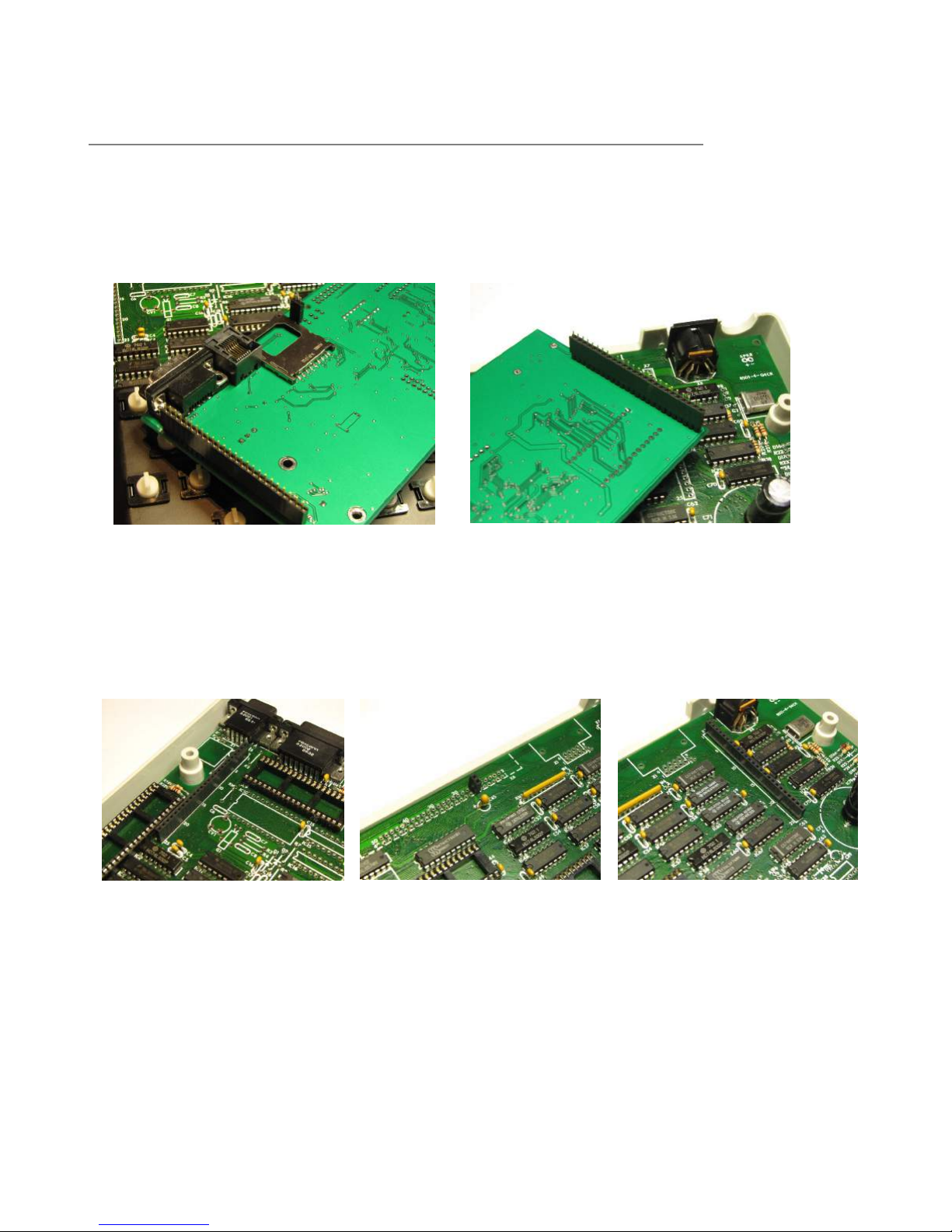
7. Core board sockets.
There are 3 sockets that need soldering onto the baseboard PCB for connection to the core
board. There are two 25 way socket stri s and one 2way socket header that must be
installed. The easiest way to get these connectors into the correct osition and ensure that
they are u right is to use the core board as a guide with the sockets lugged onto the in
stri s.
Right side 25 way stri + 2 way socket
Left side 25 way socket stri
Put the core board in location on the main board & ‘tack’ the 2 outer most ins of each 25
way socket stri first. Check that the sockets are as close to the PCB as ossible and that
the 2 way socket is in its location at ins 13 & 14 of the 50 way connector osition – X6.
Once satisfied that everything lines u correctly, solder the rest of the ins on all 3 of the
socket stri s and then remove the core board.
Page 17 of 31. Version 1.03 September 2012 Microbee Premium Plus+ | Construction Manual
8. Completing the Baseboard.
The final ste s in com leting the construction of your Microbee Premium Plus baseboard
involve com leting the installation of the key switches, fitting the key to s, fitting the
socketed com onents and wiring u the s eaker.
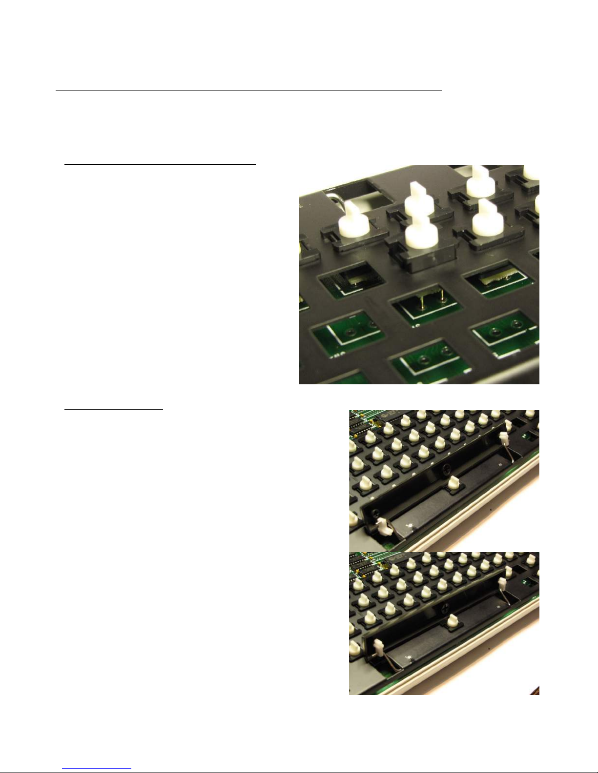
Installing the rest of the key switches
Start from the front most row when
fitting u the remaining key switches.
This enables you to look down through
the keyboard frame from the rear so
that you can see the ins of the key
switch and line them u with the holes
in the ads on the PCB. Note that the
front most row only has 5 keys and has
2 s are switch ositions closest to the
s ace bar. As you solder the key
switches in, remember to a ly just
enough heat to melt the solder and
form a decent joint on the PCB.
A lying rolonged heat to the key
switch in will melt the solder on the
switch ada ter and if excessive heat is
a lied, the in may lodge itself in the
underside of the key switch.
Fitting the key to s
Fitting the s ace bar requires several ste s :
Two white s ace bar su ort mounts have
been included in the keyboard kit. These fit to
the bottom of the s ace bar & have slots in
them to take the ends of the torsion bar.
This arrangement hel s to kee the s ace bar
level when ressed somewhere off-centre.
Fit one of these to one side of the s ace bar as
shown in the to icture to the right.
Slide that end of s ace bar with the su ort
onto the torsion bar, add a su ort to the
other end of the torsion bar & then fit the
su ort into the bottom of the s ace bar.
Now that the s ace bar & mounts are fitted to
the torsion bar, the s ace bar can be ushed
down onto the key switch and fitting the s ace
bar is done.
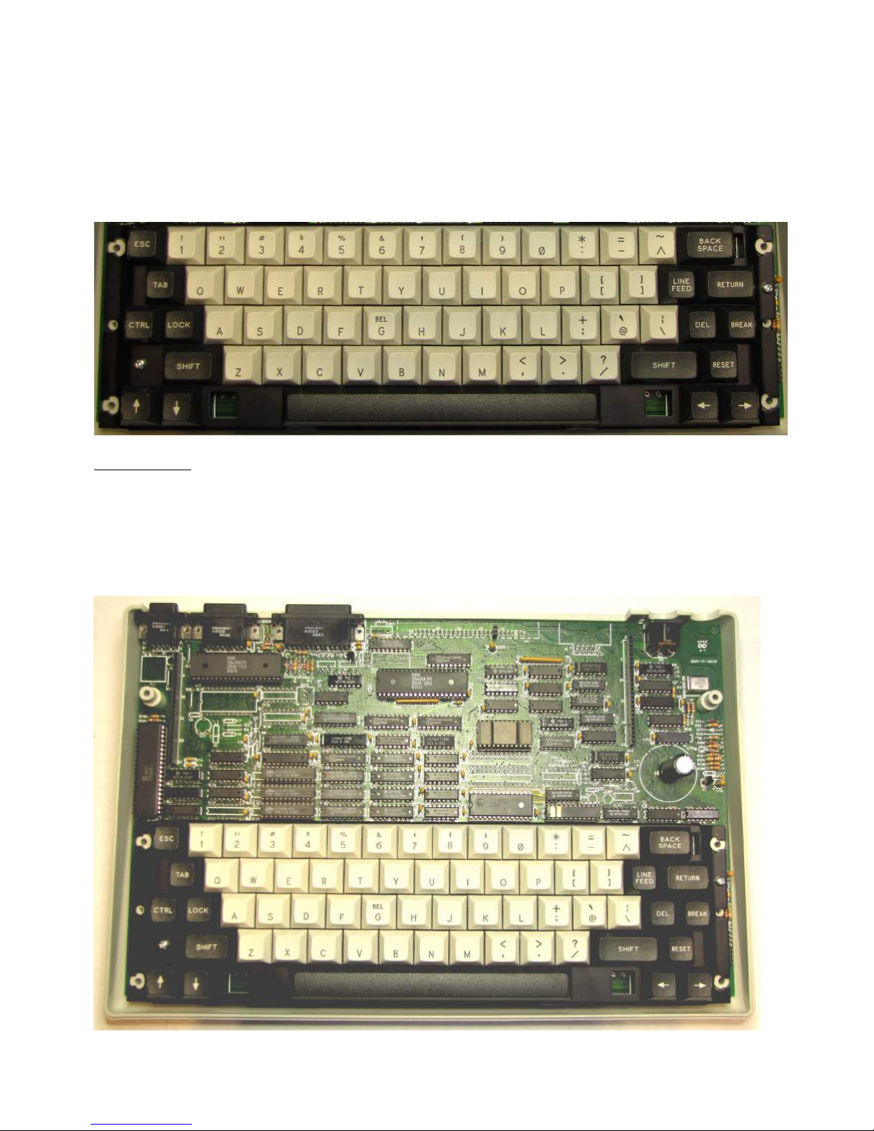
Page 18 of 31. Version 1.03 September 2012 Microbee Premium Plus+ | Construction Manual
Fitting the rest of the key to s is straight forward. Note that the arrow keys can be
interchanged with each other unlike the original key to set in which the u arrow, down,
left & right arrows were all s ecific to a articular osition.
The original keys had a ‘high side’ and ‘low side’ (i.e. they were an angled / scul ted design)
whereas the new key to s are uniform in sha e.
When finished, the keyboard should look like the icture below.
Socketed ICs
All of the remaining ICs can now be ut into their sockets. Pay attention to the orientation,
checking where Pin 1 should be located for each as you lug them in.
The ICs that are socketed are as follows:
IC1 – 6545, IC9 – Z80APIO, IC33 – Z80ACPU, IC50 – Font ROM (2532),
IC19,20 & 21 – CY7C128A, IC53/4 - CY62256 SRAM, IC61 – 74HC139 and
IC62 - the GOLD PAL
Once done, the baseboard should look like the one in the following hoto.

Page 19 of 31. Version 1.03 September 2012 Microbee Premium Plus+ | Construction Manual
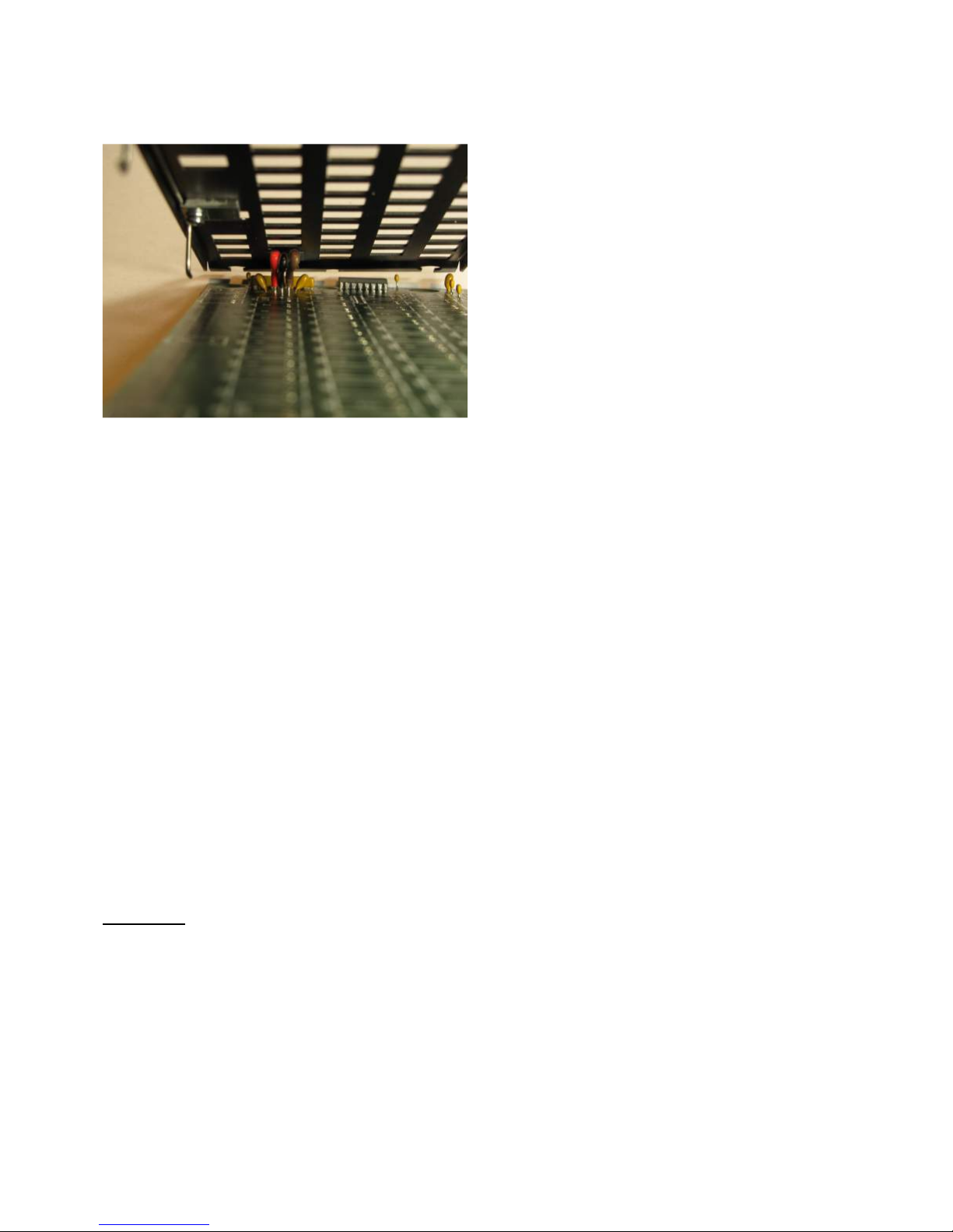
S eaker wiring
The s eaker should already be in lace in the bottom of the case held in with its metal
clam s & screws. Wiring is straight forward with the 2 core bell wire su lied. Stri both
ends of the wires, tin them with the soldering iron and attach to the s eaker and baseboard
as shown in the hotos below. The volume control for the s eaker should be set at the mid
way oint of its travel now.
Tinned Bell wire attached to the s eaker S eaker cable connected to the under-side
of the PCB near the 5 in DIN socket.
9. Final checks & first power up.
Now that all the com onents are soldered into the baseboard, it is time for final visual
ins ections, checking for shorts and un-soldered ins, com onent orientation mistakes,
olarised ca acitors & diodes the wrong way around and so on.
The check that was carried out earlier with the multimeter can be done again in checking for
a short across the in ut ower rail at C71, not that much should have changed in that area
since the revious check. It is however a sim le test & easy to carry out, so best to do it
anyway. The voltage checks can also be done, without the coreboard installed, to ensure
that the two 5 volt ower rails still rovide the required voltage.
Without the coreboard lugged in, the system will not do anything, so don’t ex ect to hear a
bee or get video on the dis lay – we just want to measure the ower rails again.
Once done, remove ower from the baseboard.
If all looks good, the coreboard can be lugged into the baseboard. Make sure that the 25
way ins stri s fit snugly into the baseboard sockets and in1 goes to in 1 (that it hasn’t
‘missed by 1’). Also make sure that the 2 ins hanging down from the coreboard near the
SDcard socket are ro erly inserted to the 2 way socket on the baseboard. If these 2 ins
do not meet with the socket ro erly, the Coldfire rocessor on the coreboard will not be
able to get the machine u & running ro erly and will have no way of gaining control of the
baseboard signal busses. Leave the SDcard out of the socket for now – it is not needed until
the after we see video out ut & run the in built self test diagnostics.

Page 20 of 31. Version 1.03 September 2012 Microbee Premium Plus+ | Construction Manual
The 5 in din lead that lugs into the Microbee has 4 lugs on the other end, or 3 & a lug
ack ower su ly. One of the other connectors on the cable is an RCA connector. This
connector rovides monochrome video out ut and can be lugged into a suitable monitor or
a television that has an ‘AV’ in ut. Connect this to the monitor / TV now and have it
switched on and ready to dis lay the boot screen of the Premium Plus.
A ly ower now (from the Plug Pak or other suitable 10 – 14 Vdc 1.5am ower su ly)
and if all is well, the RED L.E.D. on the coreboard should flash once & you should see the
boot menu on your monitor.
On the left (above) is the boot menu that a ears when there is no SDcard in the socket at
boot time (and no disk in the disk drive if you have the hysical flo y disk interface o tion
installed on the coreboard). The boot menu gives you 3 o tions – Boot disk, [machine
language] Monitor , and Self Test.
Press the ‘S’ key to activate the self test mode. It should look like the screen shot on the
right (don’t forget that you will only have monochrome video, so no color). The keyboard
test is the first item to run and for now just ress ESC twice to by ass it. All items should
ass with the exce tion of the serial and arallel ort tests which need s ecially wired
loo back lugs. The PCG Bank test should test all 15 banks of memory, and the Memory
Block test should test all 1024k of memory available to the ‘Z80 mode’ side of the Microbee.
If all is well and all the tests run through as they should, reset the machine by holding down
RESET for 1 second & enter Self test again. This time, run through the keyboard test.
The test asks you to ress each key in turn starting with ESC,1,2,3… and works down the
keyboard in rows TAB,Q,W,E,R…, CTRL, LOCK, A,S and so on.
Once you are ha y that all the self test diagnostics have assed, try re-booting the
machine with the SDcard in the slot.
To insert the SDcard, the card has to be u side-down. That is, the contacts on the card
should be facing u wards & the label on the card facing down. The SDcard connector is a
PUSH-PUSH ty e – that is, when the card is inserted, you ush it all the way in & it locks
into lace. When you want to remove the card again, you ush the card inwards again to
Table of contents


