manuals.online logo
Brands
  1. Home
  2. •
  3. Brands
  4. •
  5. Microchip Technology
  6. •
  7. Controllers
  8. •
  9. Microchip Technology MIC2125 Operating and maintenance instructions

Microchip Technology MIC2125 Operating and maintenance instructions

This manual suits for next models

1

Other Microchip Technology Controllers manuals
Microchip Technology PICtail Plus MCP25625 User manual

Microchip Technology

Microchip Technology PICtail Plus MCP25625 User manual

Microchip Technology ATWINC15x0 Series User manual

Microchip Technology

Microchip Technology ATWINC15x0 Series User manual

Microchip Technology dsPIC30F User manual

Microchip Technology

Microchip Technology dsPIC30F User manual

Microchip Technology USB2422 Operating and maintenance instructions

Microchip Technology

Microchip Technology USB2422 Operating and maintenance instructions

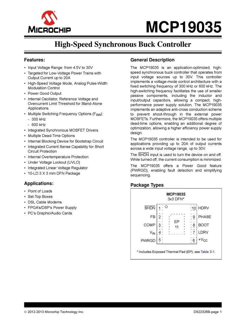
Microchip Technology MCP19035 User manual

Microchip Technology

Microchip Technology MCP19035 User manual

Microchip Technology PIC16C63A User manual

Microchip Technology

Microchip Technology PIC16C63A User manual

Microchip Technology MCP1643 User manual

Microchip Technology

Microchip Technology MCP1643 User manual

Microchip Technology PL360 User manual

Microchip Technology

Microchip Technology PL360 User manual

Microchip Technology dsPIC30F6010 User manual

Microchip Technology

Microchip Technology dsPIC30F6010 User manual

Microchip Technology MPLAB User manual

Microchip Technology

Microchip Technology MPLAB User manual

Microchip Technology MCP8063 User manual

Microchip Technology

Microchip Technology MCP8063 User manual

Microchip Technology dsPIC30F User manual

Microchip Technology

Microchip Technology dsPIC30F User manual

Microchip Technology HV9805 User manual

Microchip Technology

Microchip Technology HV9805 User manual

Microchip Technology ATWINC 15x0 Instruction Manual

Microchip Technology

Microchip Technology ATWINC 15x0 Instruction Manual

Microchip Technology ATWILC1000 User manual

Microchip Technology

Microchip Technology ATWILC1000 User manual

Microchip Technology MCP8063 User manual

Microchip Technology

Microchip Technology MCP8063 User manual

Microchip Technology dsPIC30F Reference manual
Microchip Technology

Microchip Technology dsPIC30F Reference manual

Popular Controllers manuals by other brands
Sunricher SR-ZV9003T3-RGBW-US Installation

Sunricher

Sunricher SR-ZV9003T3-RGBW-US Installation

Ksenia intro Installation and configuration manual

Ksenia

Ksenia intro Installation and configuration manual

Inovance CAN200 Series manual

Inovance

Inovance CAN200 Series manual

Gauzy LC6 FLEX Controller Installation and operation guide

Gauzy

Gauzy LC6 FLEX Controller Installation and operation guide

Viking SLP-1 Technical practice

Viking

Viking SLP-1 Technical practice

CKD KBX-30E-U Series instruction manual

CKD

CKD KBX-30E-U Series instruction manual

Sharp Energy Sun Flux User manual & installation guide

Sharp Energy

Sharp Energy Sun Flux User manual & installation guide

Yamaha RCX40 user manual

Yamaha

Yamaha RCX40 user manual

AB Quality PowerFlex 400 Frames D-H Service bulletin

AB Quality

AB Quality PowerFlex 400 Frames D-H Service bulletin

Yamaha MJC8 owner's manual

Yamaha

Yamaha MJC8 owner's manual

AL-KO ATC operating instructions

AL-KO

AL-KO ATC operating instructions

Savant SmartControl 2 Deployment guide

Savant

Savant SmartControl 2 Deployment guide

GameSir T3S user manual

GameSir

GameSir T3S user manual

Kostal inveor operating manual

Kostal

Kostal inveor operating manual

Emerson Yarway 20-55 Operating and safety instructions

Emerson

Emerson Yarway 20-55 Operating and safety instructions

CoCo ACM-LV24 Quick installation guide

CoCo

CoCo ACM-LV24 Quick installation guide

Brooks SLA5810/20 Installation and operation manual

Brooks

Brooks SLA5810/20 Installation and operation manual

SIGMA TEK SR 011 Technical manual

SIGMA TEK

SIGMA TEK SR 011 Technical manual

manuals.online logo
manuals.online logoBrands
  • About & Mission
  • Contact us
  • Privacy Policy
  • Terms and Conditions

Copyright 2025 Manuals.Online. All Rights Reserved.

2015 Microchip Technology Inc. DS20005459B-page 1
MIC2125/6
Features
• Hyper Speed Control Architecture Enables:
- High delta V operation (VIN = 28V and VOUT
= 0.6V)
- Any Capacitor™ stable
• 4.5V to 28V Input Voltage
• Adjustable Output Voltage from 0.6V to 24V
• 200 kHz to 750 kHz Programmable Switching
Frequency
• HyperLight Load®(MIC2125)
• Hyper Speed Control®(MIC2126)
• Enable Input and Power Good Output
• Built-in 5V Regulator for Single-Supply Operation
• Programmable current limit and “hiccup” mode
short-circuit protection
• 7 ms internal soft-start, internal compensation,
and thermal shutdown
• Supports Safe Start-Up into a Prebiased Output
• –40°C to +125°C Junction Temperature Range
• Available in 16-pin, 3 mm × 3 mm QFN Package
Applications
• Networking/Telecom Equipment
• Base Stations, Servers
• Distributed Power Systems
• Industrial Power Supplies
General Description
The MIC2125 and MIC2126 are constant-frequency
synchronous buck controllers featuring a unique
adaptive ON-time control architecture. The MIC2125/6
operate over an input voltage range from 4.5V to 28V
and can be used to supply load current up to 25A. The
output voltage is adjustable down to 0.6V with a
guaranteed accuracy of ±1%. The device operates with
programmable switching frequency from 200 kHz to
750 kHz.
HyperLight Load®architecture provides the same high
efficiency and ultra-fast transient response as the
Hyper Speed Control®architecture under medium to
heavy loads. It also maintains high efficiency under
light load conditions by transitioning to variable
frequency, discontinuous conduction mode operation.
The MIC2125/6 offer a full suite of features to ensure
protection of the IC during fault conditions. These
include undervoltage lockout to ensure proper
operation under power-sag conditions, internal
soft-start to reduce inrush current, “hiccup” mode
short-circuit protection, and thermal shutdown.
Package Type
MIC2125/6
16-Pin 3 mm x 3 mm QFN (ML)
VDD
PVDD
ILIM
DL
AGND
NC
OVP
BST
FB
PG
EN
VIN
SW
DH
FREQ
PGND
EP 17
1
2
3
4
56 78
12
11
10
9
16 15 14 13
28V Synchronous Buck Controllers
Featuring Adaptive ON-Time Control
MIC2125/6
DS20005459B-page 2 2015 Microchip Technology Inc.
Typical Application Circuit
Functional Block Diagram
MIC2125/6
3x3 QFN
VIN
4.5V TO 28V
2.2μF
×3 220μF
0.1μF
0.1μF
0.72μH
VOUT
3.3V/20A
90.9kΩ
1.2kΩ
10kΩ
56.2kΩ
2.26kΩ
10kΩ
470pF 100μF 470μF
4.7μF
EN
PG
VOUT
PVDD
VDD
AGND
EN
PG
OVP
FB
FREQ
VIN
BST
DH
SW
DL
PGND
ILIM
MIC2125/6
4.7μF
MIC2125/26
EN
VDD
EN
g
m
EA
COMP
CL
DETECTION
CONTROL
LOGIC
TIMER
SOFT–START
FIXED T
ON
ESTIMATE
UVLO
LDO
THERMAL
SHUTDOWN
SOFT
START
PVDD
COMPENSATION
MODIFIED
T
OFF
PG
49.9kΩ
VDD
PG
VDD
8%
92%
100kΩ
V
IN
HSD
LSD
90.9kΩ
V
OUT
3.3V/20A
0.1μF
SW
FB
470pF
DL
DH
BST
Q1
Q3
VIN
AGND
PGND
220μF
0.1μF
100μF
2.2μF
×2
0.72μH
R1
10kΩ
R2
2.26kΩ
1.2kΩ
V
IN
4.5V TO 28V
R19
R20
FREQ
ILIM
OVP
V
REF
0.6V
V
REF
0.6V
PVDD
470μF
2015 Microchip Technology Inc. DS20005459B-page 3
MIC2125/6
1.0 ELECTRICAL CHARACTERISTICS
Absolute Maximum Ratings †
VIN.............................................................................................................................................................. –0.3V to +30V
VDD, PVDD .................................................................................................................................................... –0.3V to +6V
VSW, VFREQ, VILIM, VEN ....................................................................................................................–0.3V to (VIN +0.3V)
VBST to VSW ................................................................................................................................................... –0.3V to 6V
VBST ............................................................................................................................................................. –0.3V to 36V
VPG................................................................................................................................................. –0.3V to (VDD + 0.3V)
VFB ................................................................................................................................................. –0.3V to (VDD + 0.3V)
PGND to AGND ........................................................................................................................................... –0.3V to +0.3V
ESD Rating(1)............................................................................................................................................................. 2 kV
Operating Ratings ‡
Supply Voltage (VIN) ...................................................................................................................................... 4.5V to 28V
VSW, VFREQ, VILIM, VEN ......................................................................................................................................0V to VIN
†Notice: Stresses above those listed under “Absolute Maximum Ratings” may cause permanent damage to the device.
This is a stress rating only and functional operation of the device at those or any other conditions above those indicated
in the operational sections of this specification is not intended. Exposure to maximum rating conditions for extended
periods may affect device reliability.
‡ Notice: The device is not guaranteed to function outside its operating ratings.
Note 1: Devices are ESD sensitive. Handling precautions are recommended. Human body model, 1.5 kin series
with 100 pF.
MIC2125/6
DS20005459B-page 4 2015 Microchip Technology Inc.
TABLE 1-1: ELECTRICAL CHARACTERISTICS
Electrical Characteristics: VIN = 12V, VOUT = 1.2V, VBST – VSW = 5V; TA= 25°C, unless noted. Bold values indicate
–40°C TJ+125°C. (Note 1).
Parameters Min. Typ. Max. Units Conditions
Power Supply Input
Input Voltage Range (VIN)
(Note 2)4.5 —5.5 VV
DD = VIN
4.5 —28 —
Quiescent Supply Current
(MIC2125)
—340750 µA VFB = 1.5V
Quiescent Supply Current
(MIC2126)
—1.1 3mA VFB = 1.5V
Shutdown Supply Current — 0.1 5µA SW unconnected, VEN = 0V
VDD Supply
VDD Output Voltage 4.8 5.2 5.4 VV
IN = 7V to 28V, IDD = 10 mA
VDD UVLO Threshold 3.7 4.2 4.5 VDD rising
VDD UVLO Hysteresis — 400 — mV —
Load Regulation 0.6 2 3.6 % IDD = 0 to 40 mA
Reference
Feedback Reference Voltage 0.597 0.6 0.603 V TJ= 25°C (±0.5%)
0.594 0.6 0.606 –40°C TJ+125°C (±1%)
FB Bias Current — 0.01 0.5 µA VFB = 0.6V
Enable Control
EN Logic Level High 1.6 —— V—
EN Logic Level Low — — 0.6 —
EN Hysteresis — 120 — mV —
EN Bias Current — 6 30 µA VEN = 12V
Oscillator
Switching Frequency — 750 — kHz VFREQ = VIN
—375 — V
FREQ = 50% x VIN
Maximum Duty Cycle — 85 — % —
Minimum Duty Cycle — 0 — VFB > 0.6V
Minimum On-Time — 100 — ns —
Minimum Off-Time 150 220 300 —
Soft-Start
Soft-Start Time — 7 — ms —
Short-Circuit Protection and OVP
Current-Limit Comparator
Offset
–15 –4 7 mV VFB = 0.6V
Current-Limit Source Current 32 36 40 µA VFB = 0.6V
Note 1: Specification for packaged product only.
2: The application is fully functional at low VDD (supply of the control section) if the external MOSFETs have
low voltage VTH.
2015 Microchip Technology Inc. DS20005459B-page 5
MIC2125/6
Overvoltage Protection
Threshold
—— 0.62 — V —
FET Drivers
DH, DL Output Low Voltage — — 0.1 VI
SINK = 10 mA
DH, DL Output High Voltage VPVDD-0.1
or
VBST-0.1
—— I
SOURCE = 10 mA
DH On-Resistance, High State — 2.5 — —
DH On-Resistance, Low State — 1.6 — —
DL On-Resistance, High State — 1.9 — —
DL On-Resistance, Low State — 0.55 — —
SW, BST Leakage Current — — 50 µA —
Power Good (PG)
PG Threshold Voltage 85 89 95 %VOUT Sweep VFB from low to high
PG Hysteresis — 6 — Sweep VFB from high to low
PG Delay Time — 80 — µs Sweep VFB from low to high
PG Low Voltage — 60 200 mV VFB < 90% x VNOM, IPG = 1 mA
Thermal Protection
Overtemperature Shutdown — 150 — °C TJRising
Overtemperature Shutdown
Hysteresis
—15 — °C—
TABLE 1-1: ELECTRICAL CHARACTERISTICS (CONTINUED)
Electrical Characteristics: VIN = 12V, VOUT = 1.2V, VBST – VSW = 5V; TA= 25°C, unless noted. Bold values indicate
–40°C TJ+125°C. (Note 1).
Parameters Min. Typ. Max. Units Conditions
Note 1: Specification for packaged product only.
2: The application is fully functional at low VDD (supply of the control section) if the external MOSFETs have
low voltage VTH.
MIC2125/6
DS20005459B-page 6 2015 Microchip Technology Inc.
TEMPERATURE SPECIFICATIONS
Parameters Sym. Min. Typ. Max. Units Conditions
Temperature Ranges
Junction Operating Temperature TJ–40 — +125 °C Note 1
Storage Temperature Range TS–65 — +150 °C —
Junction Temperature TJ— — +150 °C —
Lead Temperature — — — +260 °C Soldering, 10s
Package Thermal Resistances
Thermal Resistance 3 mm x 3 mm
QFN-16LD
JA —50.8 —°C/W—
JC —25.3 —°C/W—
Note 1: The maximum allowable power dissipation is a function of ambient temperature, the maximum allowable
junction temperature and the thermal resistance from junction to air (i.e., TA, TJ, JA). Exceeding the
maximum allowable power dissipation will cause the device operating junction temperature to exceed the
maximum +125°C rating. Sustained junction temperatures above +125°C can impact the device reliability.
2015 Microchip Technology Inc. DS20005459B-page 7
MIC2125/6
2.0 TYPICAL PERFORMANCE CURVES
Note: Unless otherwise noted, VIN = 12V, FREQ = 350 kHz.
FIGURE 2-1: VIN Operating Supply
Current vs. Input Voltage (MIC2125).
FIGURE 2-2: Feedback Voltage vs. Input
Voltage (MIC2125).
FIGURE 2-3: Output Voltage vs. Input
Voltage (MIC2125).
FIGURE 2-4: VIN Shutdown Current vs.
Input Voltage (MIC2125).
FIGURE 2-5: Switching Frequency vs.
Input Voltage.
FIGURE 2-6: Switching Frequency vs.
Temperature (MIC2126).
Note: The graphs and tables provided following this note are a statistical summary based on a limited number of
samples and are provided for informational purposes only. The performance characteristics listed herein
are not tested or guaranteed. In some graphs or tables, the data presented may be outside the specified
operating range (e.g., outside specified power supply range) and therefore outside the warranted range.
MIC2125/6
DS20005459B-page 8 2015 Microchip Technology Inc.
Note: Unless otherwise noted, VIN = 12V, FREQ = 350 kHz.
FIGURE 2-7: VDD Voltage vs. Input
Voltage (MIC2125).
FIGURE 2-8: Enable Threshold vs. Input
Voltage (MIC2125).
FIGURE 2-9: Output Peak Current Limit
vs. Input Voltage (MIC2125).
.V
FIGURE 2-10: VIN Operating Supply
Current vs. Temperature (MIC2125).
FIGURE 2-11: Feedback Voltage vs.
Temperature (MIC2125).
FIGURE 2-12: Load Regulation vs.
Temperature (MIC2125).
2015 Microchip Technology Inc. DS20005459B-page 9
MIC2125/6
Note: Unless otherwise noted, VIN = 12V, FREQ = 350 kHz.
FIGURE 2-13: VIN Shutdown Current vs.
Temperature (MIC2125).
FIGURE 2-14: VDD UVLO Threshold vs.
Temperature (MIC2125).
FIGURE 2-15: Enable Threshold vs.
Temperature (MIC2125).
FIGURE 2-16: EN Bias Current vs.
Temperature (MIC2125).
FIGURE 2-17: VDD Voltage vs.
Temperature (MIC2125).
FIGURE 2-18: Current-Limit Source
Current vs. Temperature (MIC2125).
MIC2125/6
DS20005459B-page 10 2015 Microchip Technology Inc.
Note: Unless otherwise noted, VIN = 12V, FREQ = 350 kHz.
*Note: For Case Temperature graphs: The temperature measurement was taken at the hottest point on the MIC2125/6
case mounted on a 5 square inch PCBn. Actual results will depend upon the size of the PCB, ambient temperature and
proximity to other heat emitting components.
FIGURE 2-19: Line Regulation vs.
Temperature (MIC2125).
FIGURE 2-20: Feedback Voltage vs.
Output Current (MIC2125).
FIGURE 2-21: Line Regulation vs. Output
Current (MIC2125).
FIGURE 2-22: Output Regulation vs. Input
Voltage (MIC2125).
FIGURE 2-23: Case Temperature* vs.
Output Current (MIC2125).
FIGURE 2-24: Case Temperature* vs.
Output Current (MIC2125).