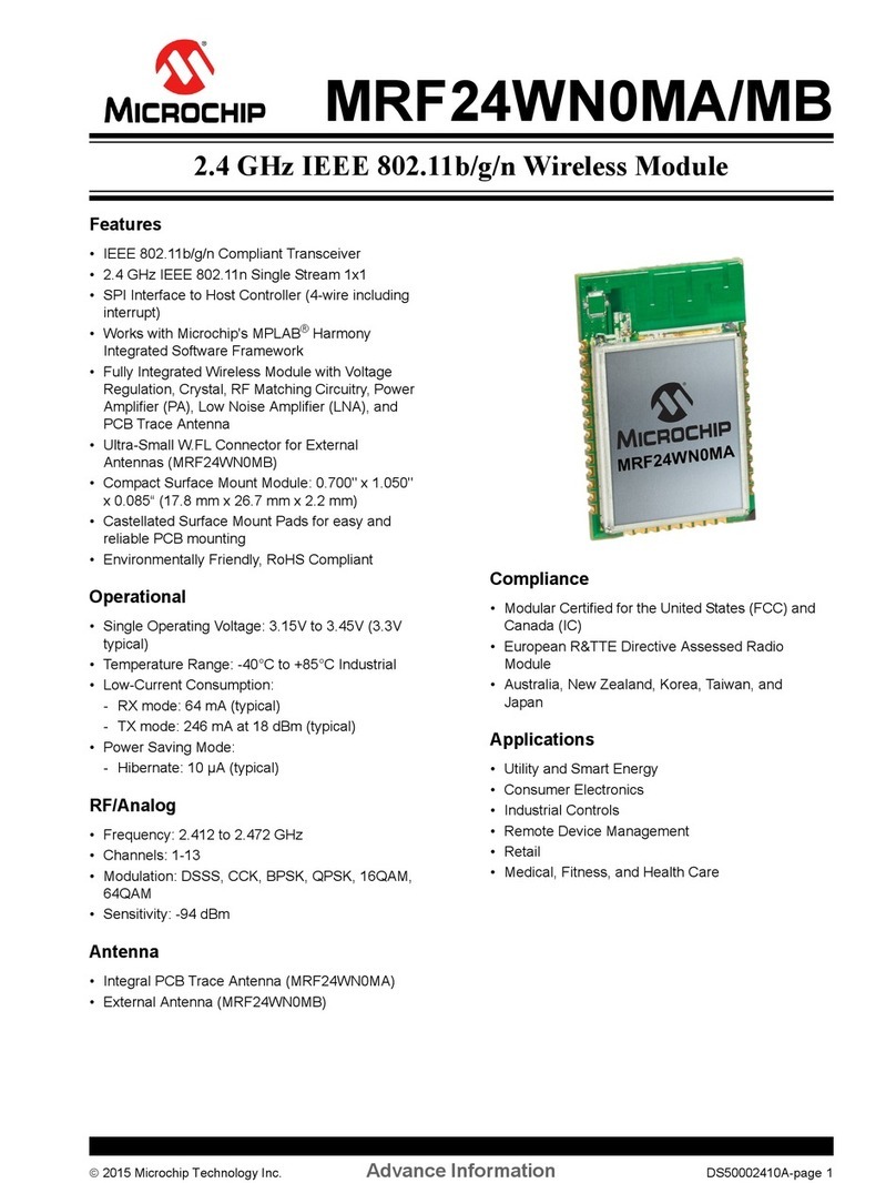
Microchip Technology RN1810 User manual

Page 1 of 2
Product Change Notification / SYST-07QSQG543
Date:
11-May-2021
Product Category:
Wireless Modules
PCN Type:
Document Change
Notification Subject:
Data Sheet - RN1810/RN1810E 2.4 GHz IEEE 802.11b/g/n Wireless Module Data Sheet
Affected CPNs:
SYST-07QSQG543_Affected_CPN_05112021.pdf
SYST-07QSQG543_Affected_CPN_05112021.csv
Notification Text:
SYST-07QSQG543
Microchip has released a new Product Documents for the RN1810/RN1810E 2.4 GHz IEEE 802.11b/g/n Wireless Module Data Sheet of
devices. If you are using one of these devices please read the document located at RN1810/ RN1810E 2.4 GHz IEEE 802.11b/ g/ n
Wir eless Module Data Sheet.
Notification Status: Final
Description of Change:
1) Updated Section 4.2 “Canada” and Section 4.3 “Europe”
Impacts to Data Sheet: None
Reason for Change: To Improve Manufacturability
Change Implementation Status: Complete
Date Document Changes Effective: 11 May 2021
NOTE: Please be advised that this is a change to the document only the product has not been changed.
Markings to Distinguish Revised from Unrevised Devices: N/A

Attachments:
RN1810/ RN1810E 2.4 GHz IEEE 802.11b/ g/ n Wir eless Module Data Sheet
Please contact your local Microchip sales office with questions or concerns regarding this notification.
Terms and Conditions:
If you wish to receive Microchip PCNs via email please register for our PCN email service at our PCN
home page select register then fill in the required fields. You will find instructions about registering for
Microchips PCN email service in the PCN FAQ
section.
If you wish to change your PCN profile, including opt out, please go to the PCN home page select login
and sign into your myMicrochip account. Select a profile option from the left navigation bar and make
the applicable selections.

Affected Catalog Part Numbers (CPN)
RN1810-I/RM100
RN1810-I/RM110
RN1810E-I/RM100
RN1810E-I/RM110
SYST-07QSQG543 - Data Sheet - RN1810/RN1810E 2.4 GHz IEEE 802.11b/g/n Wireless Module Data Sheet
Date: Monday, May 10, 2021

SYST-07QSQG543 - Data Sheet - RN1810/RN1810E 2.4 GHz IEEE 802.11b/g/n Wireless Module Data Sheet
Affected Catalog Part Numbers(CPN)
RN1810-I/RM100
RN1810-I/RM110
RN1810E-I/RM100
RN1810E-I/RM110

2016-2021 Microchip Technology Inc. DS50002460C-page 1
RN1810/RN1810E
Features
• IEEE 802.11b/g/n Compliant Transceiver
• 2.4 GHz IEEE 802.11n Single Stream 1x1
• UART Interface to Host Controller (4-wire
including RTS/CTS)
• Integrates Easily into Final Product - Minimizes
Product Development, Provides Quicker Time to
Market
• Configured using Simple ASCII Commands
• Fully Integrated Wireless Module with Voltage
Regulation, Crystal, RF Matching Circuitry, Power
Amplifier (PA), Low Noise Amplifier (LNA) and
PCB Trace Antenna
• Ultra-Small W.FL Connector for External
Antennas (RN1810E)
• Compact Surface Mount Module: 0.700" x 1.050"
x 0.085" (17.8 mm x 26.7 mm x 2.2 mm)
• Castellated Surface Mount Pads for easy and
reliable PCB mounting
• Environmentally Friendly, RoHS Compliant
Operational
• Single Operating Voltage: 3.15V to 3.45V (3.3V
typical)
• Temperature Range: -40°C to +85°C Industrial
• Low-Current Consumption:
- RX mode: 64 mA (typical)
- TX mode: 246 mA at 18 dBm (typical)
• Power Saving Mode:
- Sleep: 12 µA (typical)
RF/Analog
• Frequency: 2.412 to 2.472 GHz
• Channels: 1-13
• Modulation: DSSS, CCK, BPSK, QPSK, 16QAM
and 64QAM
• Sensitivity: -94 dBm
Antenna
• Integral PCB Trace Antenna (RN1810)
• External Antenna (RN1810E)
Compliance
• Modular Certified for the United States (FCC) and
Canada (IC)
• European R&TTE Directive Assessed Radio
Module
• Australia, New Zealand, Korea, Taiwan and Japan
Applications
• Utility and Smart Energy
• Consumer Electronics
• Industrial Controls
• Remote Device Management
• Retail
• Medical, Fitness and Health Care
Networking
• Supports Infrastructure and SoftAp Networking
Modes
• Built-In Networking Applications: IPv4/IPv6, TCP,
UDP, DHCP, DNS, ICMP, ARP, HTTP, FTP, SNTP
and SSL/TLS
• Complete On-Board TCP/IP Networking
• Upgrade Firmware Over the Air using TFTP
• Supports Wi-Fi®Protected Setup (WPS)
2.4 GHz IEEE 802.11b/g/n Wireless Module

RN1810/RN1810E
DS50002460C-page 2 2016-2021 Microchip Technology Inc.
NOTES:

2016-2021 Microchip Technology Inc. DS50002460C-page 3
RN1810/RN1810E
1.0 DEVICE OVERVIEW
The RN1810 and RN1810E are low-power, 2.4 GHz,
IEEE 802.11n compliant, surface mount modules
containing all associated RF components: crystal
oscillator, bypass and bias passives with integrated
MAC, baseband, RF and power amplifier and built-in
hardware support for encryption. Refer to Figure 1-1.
The integrated module design frees the designer from
RF and antenna design tasks and regulatory compli-
ance testing, ultimately providing faster time to market.
RN1810 incorporates an on-board TCP/IP networking
stack, cryptographic accelerator, power management
subsystem, real-time clock, 2.4 GHz transceiver and
RF power amplifier. With the module, designers can
embed Wi-Fi and networking functionality rapidly into
virtually any device.
The RN1810 provides cost and time-to-market savings
as a self-contained Internet-enabling solution. The
module has been designed to provide designers with a
simple Wi-Fi solution that features:
• Ease of integration and programming
• Vastly reduced development time
• Minimum system cost
• Long battery life
• Maximum value in a range of applications
The RN1810 is configured with a simple ASCII com-
mand language.
In the simplest configuration, the module requires only
power, ground and UART TX and RX connections. The
RN1810 module can interface to low-cost microcontrol-
lers using only two wires, UART TX and RX.
The RN1810 can independently maintain a low-power
wireless network connection. Ultra-low power usage
and flexible power management maximize the mod-
ule's lifetime in battery-operated devices. A wide oper-
ating temperature range allows use in indoor and
outdoor environments (industrial temperature range).
When operating in Sleep mode, the module minimizes
battery usage while still being able to respond to certain
events, including internal timers and WAKEUP signal.
Applications that make efficient use of the Sleep state
can extend battery life to multiple years.
The RN1810 module is approved for use with the inte-
grated PCB trace antenna. The RN1810E module is
approved for use with specific external antenna types
that are certified with the module. An ultra-small coaxial
connector (W.FL) is provided on the module for con-
nection to the external antenna. Refer to Section 3.3,
"External Antenna Types" for a listing of approved
antenna types.
The RN1810/RN1810E modules received the
regulatory approvals for modular devices in the United
States (FCC) and Canada (IC). Modular approval
removes the need for expensive RF and antenna
design, and enables the end user to place the RN1810/
RN1810E modules inside a finished product without
requiring a regulatory testing for an intentional radiator
(RF transmitter).
The RN1810/RN1810E module is an R&TTE Directive
assessed radio module for operation in Europe. The
module tests can be applied toward final product
certification and Declaration of Conformity (DoC).
Table 1-1 lists the RN1810 module's family types.
TABLE 1-1: RN1810 FAMILY TYPES
Device Antenna
RN1810 Integral
RN1810E External
RN1810/RN1810E
DS50002460C-page 4 2016-2021 Microchip Technology Inc.
FIGURE 1-1: RN1810/RN1810E BLOCK DIAGRAM
Matching
Circuitry
Wi-Fi
SoC
Flash
PCB Trace
Antenna
(RN1810)
External Antenna
Connector
(RN1810E)
Power/Ground
RN1810/RN1810E 2.4 GHz IEEE 802.11 b/g/n Module
UART
Sleep/Wakeup/
Reset/Control
Event/Status

RN1810/RN1810E
DS50002460C-page 6 2016-2021 Microchip Technology Inc.
TABLE 1-2: PIN DESCRIPTIONS
Pin Name Type Description(1)
1 GND Power —
2 TEST Test Do not connect
3 GND Power —
4V
DD Power —
5 CMD_STATUS DO This is an optional IO that signals operational status.
6 STATUS_RDY DO This is an optional IO that signals WiFly is ready to accept commands.
7 UART0_TX DO Host interface UART0 TX
8 IP_STATUS DO This is an optional IO that signals WiFly has connected to an AP and
received an IP address.
9 UART0_CTS DI UART0 CTS
10 UART0_RTS DO UART0 RTS
11 NC Reserved Do not connect
12 TCP_STATUS DO This an optional IO that signals a successful TCP connection or FTP
transfer.
13 SLEEP DI This is an optional IO that puts the RN1810 into Sleep state.
14 FUNC_CONFIG DI This is an optional IO that starts various applications and resets
configurations to factory defaults.
15 VDD Power —
16 GND Power —
17 TEST Test Do not connect
18 TEST Test Do not connect
19 RESETDI Resets RN1810
20 CMD_CTRL DI This is an optional IO that switches RN1810 modes.
21 UART0_RX/
MODE0
DI Host interface UART0 RX/Mode select 0; connect to VDD via 100 kpull-up
resistor(2)
22 TCP_CTRL DI This is an optional IO that opens or closes a TCP connection or hand-
shakes FTP transfers.
23 MODE1 DI Mode select 1; connect to GND(2)
24 GND Power —
25 WAKEUP DI This is an optional IO that awakens the RN1810 from Sleep mode.
26 MISC_STATUS DO This is an optional IO that signals miscellaneous application status.
27 GND Power —
28 NC Reserved Do not connect
29 NC Reserved Do not connect
30 NC Reserved Do not connect
31 NC Reserved Do not connect
32 NC Reserved Do not connect
33 NC Reserved Do not connect
34 GND Power —
35 VDD Power —
36 GND Power —
37 GND Power —
Legend: A = Analog, D = Digital, I = Input, O = Output
Note 1: For NC = No Connect pins, do not make any connection. The module is configured with internal pull-up
and pull-down resistors.
2: Refer to Section 2.2, "MODE0 and MODE1 Pins".

2016-2021 Microchip Technology Inc. DS50002460C-page 7
RN1810/RN1810E
1.2 Mounting Details
Figure 1-3, Figure 1-4 and Figure 1-5 show the physical dimensions and the mounting details of the module.
Figure 1-6 and Figure 1-7 show the recommended host PCB footprint and layout.
FIGURE 1-3: RN1810/RN1810E MODULE PHYSICAL DIMENSIONS (TOP AND SIDE VIEW)
'LPHQVLRQVDUHLQLQFKHV7ROHUDQFHV3&%RXWOLQH3&%WKLFNQHVV

RN1810/RN1810E
DS50002460C-page 8 2016-2021 Microchip Technology Inc.
FIGURE 1-4: RN1810/RN1810E MODULE PHYSICAL DIMENSIONS (BOTTOM VIEW)
'LPHQVLRQVDUHLQLQFKHV

2016-2021 Microchip Technology Inc. DS50002460C-page 9
RN1810/RN1810E
FIGURE 1-5: RN1810/RN1810E MODULE MOUNTING DETAILS
Keep area around antenna
(approximately 1.25 inches) clear
of metallic structures for
best performance.
1.25
1.25
Edge of
Host PCB
Ground Plane
0.2550.795
(Top View)
Dimensions are in inches

RN1810/RN1810E
DS50002460C-page 10 2016-2021 Microchip Technology Inc.
FIGURE 1-6: RN1810/RN1810E RECOMMENDED HOST PCB FOOTPRINT
*URXQG3ODQH+RVW3&%(GJH6KLHOG3DGV;GLDPHWHU'RQRWORFDWHG+RVW3&%WRSOD\HUFRSSHUXQGHU6KLHOG3DGV.HHSRXWDUHD'LPHQVLRQVDUHLQLQFKHV

2016-2021 Microchip Technology Inc. DS50002460C-page 11
RN1810/RN1810E
FIGURE 1-7: RN1810/RN1810E HOST PCB EXAMPLE LAYOUT
1.3 Soldering Recommendations
The RN1810/RN1810E wireless module is assembled
using the IPC/JEDEC J-STD-020 Standard lead-free
reflow profile. The RN1810/RN1810E module can be
soldered to the host PCB using standard leaded and
lead-free solder reflow profiles.
To avoid damaging the module, adhere to the following
recommendations:
• Solder reflow recommendations are provided in
the Microchip Application Note, AN233 “Solder
Reflow Recommendation” (DS00233)
• Do not exceed a peak temperature (TP) of 250°C
• Refer to the solder paste data sheet for specific
reflow profile recommendations from the vendor
• Use no-clean flux solder paste
• Do not wash as moisture can be trapped under
the shield
• Use only one flow. If the PCB requires multiple
flows, apply the module on the final flow.
Best
Good Good
Good
No Copper
in these Areas

RN1810/RN1810E
DS50002460C-page 12 2016-2021 Microchip Technology Inc.
NOTES:

2016-2021 Microchip Technology Inc. DS50002460C-page 13
RN1810/RN1810E
2.0 CIRCUIT DESCRIPTION
2.1 UART Interface
The UART interface supports 2-wire (RX, TX) and 4-
wire configurations with hardware flow control (RX, TX,
CTS and RTS) as illustrated in Figure 2-1. The logic
levels are CMOS voltage levels (not RS-232 voltage
levels). The UART interface supports baud rates of
9,600, 19,200, 38,400, 57,600 and 115,200 bits per
second.
FIGURE 2-1: HOST MCU TO RN1810/RN1810E BLOCK DIAGRAM
FIGURE 2-2: MCU TO RN1810 INTERFACE
Sleep/Wakeup/
Reset/Control
Events/Status
Application(s)
UART Driver
Any MCU
UART
RN1810/RN1810E
Power
Ground
TX
RX
RTS
CTS
RX
TX
CTS(1)
RTS(1)
MCU RN1810
Note 1: Hardware flow control is recommended for all baud rates, especially for
57,600 or greater.

RN1810/RN1810E
DS50002460C-page 14 2016-2021 Microchip Technology Inc.
2.2 MODE0 and MODE1 Pins
The MODE pins must be tied to the voltage levels for
normal operation of the module. Refer to Table 2-1.
The MODE pins are sampled at power on and wake-
up. Refer to Section 2.4, "Sleep and Wakeup". In the
case of UART0_RX/MODE0 pin, a 100 kpull-up
resistor is required, and the host MCU allows an active-
high signal during power on and wake-up to ensure that
the module start-up in normal operation. Once the
module is operational, the pin becomes the
UART0_RX pin.
2.3 VDD and GND Pin
The RN1810/RN1810E wireless module contains an
integrated power management unit that generates all
necessary voltages required by the internal circuitry.
The module is powered from a single voltage source.
Table 2-2 lists the recommended bypass capacitors.
The capacitors must be closely placed to the module.
2.4 Sleep and Wakeup
The module enters the lowest power mode when the
SLEEP pin is asserted high. WLAN and network
connection information is preserved.
The module can wake-up when WAKEUP pin is
asserted low. The module restores the saved
information after wakeup.
2.5 Module Reset
There are several ways to Reset the module:
• A Power-On Reset is automatically generated
when power is applied. This Reset is intended to
initialize the module when a new battery is
connected.
• Perform an external Power-On Reset by asserting
the RESET pin low.
• Perform a soft Power-On Reset using software
commands
The RESET pulse duration must be a minimum of
650 ns.
2.6 Factory Reset
The Factory Reset is intended to initialize provisioning
information stored in flash memory by asserting
FUNC_CONFIG Low to High five times with 300 ms
between transitions.
TABLE 2-1: MODE PIN OPERATION
Pin Condition
MODE1 Connect to GND
UART0_RX/MODE0 Connect to VDD via
100 kpull-up resistor
TABLE 2-2: RECOMMENDED BYPASS
CAPACITORS
Pin Symbol Bypass Capacitors
4VDD 0.1 µF and 2.2 µF
15 VDD 0.1 µF and 2.2 µF
35 VDD 0.1 µF and 2.2 µF

2016-2021 Microchip Technology Inc. DS50002460C-page 15
RN1810/RN1810E
3.0 APPLICATION INFORMATION
This section provides information on the Application Schematic, Integral PCB Trace Antenna and Antenna Types.
3.1 Application Schematic
Figure 3-1 shows the schematic for the RN1810/RN1810E module.
FIGURE 3-1: APPLICATION SCHEMATIC
Note 1: Refer to Table 1-2: "PIN Descriptions".
2: Hardware flow control is recommended for all baud rates, especially
for 57,600 or greater.
3: The default firmware bootup UART baud settings is 9,600 with
hardware flow control disabled.

RN1810/RN1810E
DS50002460C-page 16 2016-2021 Microchip Technology Inc.
3.2 Integral PCB Trace Antenna
For the RN1810, the PCB antenna is fabricated on the
top copper layer and covered in solder mask. The lay-
ers below the antenna do not have copper trace.
It is recommended that the module is mounted on the
edge of the host PCB. It is permitted for PCB material
to be below the antenna structure of the module as long
as no copper traces or planes are on the host PCB in
that area. For best performance, place the module on
the host PCB according to the details shown in
Figure 1-7.
The antenna patterns plotted in Figure 3-2 through
Figure 3-5 are the simulated results of the PCB
antenna.
Figure 3-2 illustrates the simulation drawing. The two-
dimensional (2D) radiation pattern is illustrated in
Figure 3-3, whereas Figure 3-4 and Figure 3-5 show
the three-dimensional (3D) radiation patterns.
The calculated average of the radiated field is shown in
Figure 3-3. The radiation pattern for the XZ plane is
shown in red, whereas the YZ plane is shown in violet.
The most powerful radiation occurs in the XZ plane as
represented by the red pattern.
Figure 3-4 shows the relative position of the 3D radia-
tion “donut” with reference to the module orientation.
This is a very useful guide for placement of the module
to obtain the maximum range.
Figure 3-5 shows the 3D radiation pattern with the
colored distribution of the radiation magnitude. The
values range from -9 dB to +0.3 dB. This is very useful
in interpreting the 2D radiation pattern.
FIGURE 3-2: PCB ANTENNA SIMULATION DRAWING
Other manuals for RN1810
1
This manual suits for next models
5
Table of contents
Other Microchip Technology Wireless Module manuals
Popular Wireless Module manuals by other brands

Velleman
Velleman Whadda WPI469 manual

SMC Networks
SMC Networks JI5-RT539222SB24 user manual

Telit Wireless Solutions
Telit Wireless Solutions LE910C series user guide

Ebyte
Ebyte E330-400T13S user manual

Telit Wireless Solutions
Telit Wireless Solutions GL865-DUAL V3 Hardware user's guide

Foxconn
Foxconn WBUR56 manual