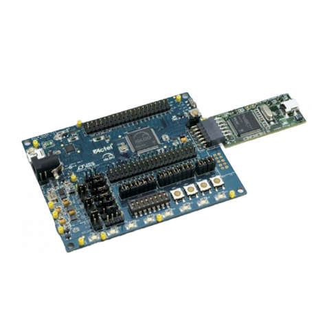
Micron Xccela Flash User manual

Micron®Xccela™Flash User Guide for ZedBoard™
This development kit (including daughterboard with FPGA software code) contains confidential information of Micron
Technology, Inc. It is provided for evaluation purposes only and is not authorized or licensed for any other use. This
development kit is provided “as is” without any warranties of any kind whatsoever. By your acceptance and use of
this development kit, you acknowledge, agree, and accept that Micron expressly disclaims all warranties, whether
written or implied by law, including warranties as to title, merchantability or fitness for a particular purpose, warranties
against infringement of intellectual property rights of a third party, warranties arising by custom, trade usage, course
of dealing, or otherwise. Micron makes no warranty of any kind, and hereby disclaims any warranty, that the
development kit will meet your or any other person’s requirements, achieve any intended result, or be secure,
accurate, complete, free of harmful code or error free. Any open source components or other third-party materials
are provided “as is” and without any representation or warranty from Micron.
Micron®Xccela™ Flash (MT35X)
Development Kit
User Guide for ZedBoard
™

CCM005-1718347970-10451
micron_xccela_zedboard_user_guide.pdf Rev 2.1 4/19 2
Micron®Xccela™Flash User Guide for ZedBoard™
Contents
1Introduction .............................................................................................................................................................3
1.1 Block Diagram................................................................................................................................................4
1.2 Zynq Bank Pin Assignments ..........................................................................................................................4
2Daughterboard Support ..........................................................................................................................................5
2.1 Daughterboard with TBGA-24 Socket (FMC_0007_SNOR_TBGA_V2.0)......................................................5
3Set Up and Installation............................................................................................................................................6
3.1 Boot File.........................................................................................................................................................6
3.2 Jumpers and Connections .............................................................................................................................6
3.3 Power Up .......................................................................................................................................................7
4. Test Routines..........................................................................................................................................................9
4.1 Command Operation......................................................................................................................................9
4.2 Key Notes Before Testing ..............................................................................................................................9
4.2 Timing Tuning ..............................................................................................................................................10
4.3 Programmer-Like Tool .................................................................................................................................10
4.3.1 Program ............................................................................................................................................11
4.3.2 Read..................................................................................................................................................11
5Revision History ....................................................................................................................................................12
Appendix A: Command List...................................................................................................................................13
Appendix B: Example Command Sequence .........................................................................................................16
Appendix C: FMC_0007_SNOR_TBGA_V2.0 Schematic.....................................................................................19

CCM005-1718347970-10451
micron_xccela_zedboard_user_guide.pdf Rev 2.1 4/19 3
Micron®Xccela™Flash User Guide for ZedBoard™
1 Introduction
The ZedBoard is an evaluation and development board based on the Xilinx Zynq™-7000 All
Programmable SoC (AP SoC). Combining a dual Cortex-A9 processing system (PS) with 85,000
Series-7 programmable logic (PL) cells, the Zynq-7000 AP SoC can be targeted for broad use in
many applications. The ZedBoard’s mix of on-board peripherals and expansion capabilities make it
an ideal platform for both novice and experienced designers. The features provided by the
ZedBoard consist of the following:
Feature
Description
Xilinx® XC7Z020-1CLG484CES
Zynq-7000 AP SoC
Primary configuration = QSPI flash
Auxiliary configuration options:
-Cascaded JTAG
-SD card
Memory -512MB DDR3 (128M x 32)
-256Mb QSPI flash
Interfaces -USB-JTAG programming using Digilent SMT1-equivalent circuit
-Accesses PL JTAG
-PS JTAG pins connected through PS Pmod
-10/100/1G Ethernet
-USB OTG 2.0
-SD card
-USB 2.0 FS USB-UART bridge
-Five Digilent Pmod™ compatible headers (2x6) (1 PS, 4 PL)
-One LPC FMC
-One AMS header
-Two reset buttons (1 PS, 1 PL)
-Seven push buttons (2 PS, 5 PL)
-Eight dip/slide switches (PL)
-Nine user LEDs (1 PS, 8 PL)
-DONE LED (PL)
Onboard Oscillators -33.333 MHz (PS)
-100 MHz (PL)
Display/Audio -HDMI output
-VGA (12-bit color)
-128x32 OLED display
-Audio line-in, line-out, headphone, microphone
Power -On/off switch
-12V @ 5A AC/DC regulator

CCM005-1718347970-10451
micron_xccela_zedboard_user_guide.pdf Rev 2.1 4/19 4
Micron®Xccela™Flash User Guide for ZedBoard™
1.1 Block Diagram
Figure 1: ZedBoard Block Diagram
1.2 Zynq Bank Pin Assignments
Figure 2: ZedBoard Z7020 CLG484 Bank Assignments

CCM005-1718347970-10451
micron_xccela_zedboard_user_guide.pdf Rev 2.1 4/19 5
Micron®Xccela™Flash User Guide for ZedBoard™
2 Daughterboard Support
A 24-ball TBGA (TBGA-24B) package for Xccela Flash is supported on a dedicated daughterboard,
which can be connected to the ZedBoard for testing.
2.1 Daughterboard with TBGA-24 Socket (FMC_0007_SNOR_TBGA_V2.0)
TBGA-24B (6mm x 8mm, 5x5 ball grid array) is supported on FMC_0007_SNOR_TBGA_V2.0, while
signal test port is also reserved on the daughterboard.
Figure 3: Daughterboard with TBGA-24 Socket
SW1 and SW2 are used for pull-up/pull-down for HOLD# and WP#. These two switches must be
configured as follows:
FMC_0007_SNOR_TBGA V2.0 Setting
SW Description Setting
SW1 HOLD# pull up/down SW1-1 on, SW1-2 off (pull-up on, pull-down off)
SW2 WP# pull up/down SW1-1 off, SW1-2 on (pull-up on, pull-down off)
IMPORTANT: The two sub-switches on SW1 and SW2 cannot be enabled at the same time;
this would cause the power to be short to ground.

CCM005-1718347970-10451
micron_xccela_zedboard_user_guide.pdf Rev 2.1 4/19 6
Micron®Xccela™Flash User Guide for ZedBoard™
3 Set Up and Installation
3.1 Boot File
The software file (config-MT35X_1.8.zip for MT35XU series or config-MT35X_3.0.zip for MT35XL series)
contains seven files required to boot up the ZedBoard. These files must be stored in a FAT32-formatted SD
card: Linux kernel, Ramdisk rootfs, device tree, boot images and testing bench-related files.
Figure 4: Boot File Contents
IMPORTANT: Do not rename the boot files; these file names must remain as displayed.
3.2 Jumpers and Connections
To boot the ZedBoard, several jumpers and connections must be configured as described below.
Follow these instructions before powering on the board.
Figure 5: ZedBoard Jumpers and Connections
1. Connect J2.
2. Configure JP7, JP8, JP10 and JP11 as follows:
Jumper
JP7
JP8
JP9
JP10
JP11
Setting
GND
GND
3V3
3V3
GND
3. Set J18 to 1V or 3V according to the operating power of your sNOR device.
Figure 6: J18 Power Setting

CCM005-1718347970-10451
micron_xccela_zedboard_user_guide.pdf Rev 2.1 4/19 7
Micron®Xccela™Flash User Guide for ZedBoard™
3.3 Power Up
1. Plug in the SD card, USB cable (for the serial port), and DC adapter as shown below.
Figure 7: SD Card, USB Cable, DC Adapter Connections
2. Switch on power by SW8.
3. If this is the first time inserting the USB port, the driver automatically downloads and installs. After
the driver installs successfully, the USB port maps to a serial port (for example, COM11).
Figure 8: Driver Software Successfully Installed
4. Open the serial port tool, and then configure the port number to the USB serial port mapped in the
previous step (for example, COM 11).
5. Set the baud rate to 115200.
Figure 9: Baud Rate Setting

CCM005-1718347970-10451
micron_xccela_zedboard_user_guide.pdf Rev 2.1 4/19 8
Micron®Xccela™Flash User Guide for ZedBoard™
ZedBoard OLEDs after boot
MT35X logo indicates the DUT
is under testing
6. If this is the first time booting the ZedBoard, run the following two commands to set up the system
boot environment, and then power down the board. Skip these three steps if you've previously
booted the ZedBoard.
•Press any key when the message Hit any key to stop autoboot appears.
•env default -f -a
•env save
Figure 10: Setting the System Boot Environment
7. Power on the ZedBoard.
When the XCCELA>> prompt appears after the Micron welcome screen (it may take a few
seconds), the system boots successfully and enters the SPI NOR test bench.
Figure 11: Xccela Flash Test Bench
Figure 12: LEDs After Booting
If another vendor’s memory is detected (instead of Micron’s Xccela family memory), or if no
memory is detected, the system hangs at the boot stage with the following message:

CCM005-1718347970-10451
micron_xccela_zedboard_user_guide.pdf Rev 2.1 4/19 9
Micron®Xccela™Flash User Guide for ZedBoard™
4. Test Routines
4.1 Command Operation
Type HELP and then press enter to obtain all supported commands for the Xccela device.
Figure 13: Xccela Commands
Type -H and then press enter to obtain command details. (For example, type FRD -H to obtain
information for the page program command.)
Figure 14: Xccela Command Details
See Appendix A: Command List for detailed command usage.
4.2 Key Notes Before Testing
Before testing, review the following important notes:
•There are three types of predefined data patterns (select by argument [pattern]) in PP commands:
-Fixed pattern: fixed data could be full 0x0 ~ 0xFF relying on value set for [pattern]
-Counter Pattern: 0x0, 0x1, 0x2, … 0xFF, 0x0, 0x1, 0x2, …
-Tuning Data Pattern (TDP): See Timing Tuning section for details
•The tuning operation is always required with the Xccela ZedBoard tool if you want to change the
frequency or data rate mode (SDR to DDR, DDR to SDR, Extended to Octal, Octal to Extended).
See the Timing Tuning section for instructions.
•The highest frequency is up to 200 MHz DDR mode; other typical frequencies are supported by
the TUNING command.
•TUNING Dxxx xx should be issued before entering Octal DDR mode.
•TUNING Sxxx xx is required before switching from Octal DDR mode to Extended mode.
•The OCTALVFY command is implemented to verify program and read functions under Octal
DDR mode, before which Octal DDR mode must be enabled.
•With the MSE command, only the SECTOR ERASE feature is enabled for multisector erase
operation. SECTOR, SUBSECTOR and BULK ERASE are all enabled in the SE command.
•No security features are supported in the current version.
CCM005-1718347970-10451
micron_xccela_zedboard_user_guide.pdf Rev 2.1 4/19 10
Micron®Xccela™Flash User Guide for ZedBoard™
4.2 Timing Tuning
After power up, the Xccela ZedBoard runs at 25 MHz SDR mode by default. The system enters 25 MHz
SDR mode as well once RESET is executed or the tuning operation is unsuccessful.
The TUNING [mode+freq] [sectornum] command tunes DUT with the expected mode (SDR or DDR)
and frequency for the SPI controller with the following options:
•S50: SDR 50MHz
•D50: DDR 50MHz
•S133: SDR 133MHz
•D133: DDR 133MHz
•S166: SDR 166MHz
•D166: DDR 166MHz
•D200: DDR 200MHz
Below is the TDP used for the Xccela ZedBoard tool:
FF0F FF00 FFCC C3CC C33C CCFF FEFF FEEF
FFDF FFDD FFFB FFFB BFFF 7FFF 77F7 BDEF
FFF0 FFF0 0FFC CC3C CC33 CCCF FEFF FFEE
FFFD FFFD DFFF BFFF BBFF F7FF F77F 7BDE
See Appendix B Example Command Sequence for a sample of the entire sequence.
4.3 Programmer-Like Tool
1. Press any key once you see the Hit any key to stop autoboot message.
2. When the Zynq> prompt appears, type run programmer
Figure 15: Running the Programmer-Like Tool
3. The programmer tool is ready when the welcome screen appears:
Figure 16: Programmer Tool Welcome Screen

CCM005-1718347970-10451
micron_xccela_zedboard_user_guide.pdf Rev 2.1 4/19 11
Micron®Xccela™Flash User Guide for ZedBoard™
4.3.1 Program
Step 1: erase
spi_programmer erase <device> <offset> <len>
device: mtd0
offset: depends on where you want to start erasing
len: erasing size
For example: Erase flash from address 0x0 to 0x20000>
zynq> spi_programmer erase /dev/mtd0 0 0x20000
Erased 131072 bytes from address 0x00000000 in flash
Step 2: program data from source file (source file is stored in SD card)
spi_programmer write <device> <offset> <len> <source-filename>
device: mtd0
offset: depends on where you want to start programming
len: length to program
source-filename: your input file
For example: Program uImage from SD card to flash, from 0x0 to 0x20000
zynq> spi_programmer write /dev/mtd0 0 0x20000 /sdcard/uImage
Copied 131072 bytes from /sdcard/uImage to address 0x00000000 in flash
4.3.2 Read
spi_programmer read <device> <offset> <len> <dest-filename>
device: mtd0
offset: the start reading address in spi nor
len: length
dest-filename: the file name of saving data
For example: Dump flash data (from address 0 to 0x20000) to SD card:
zynq> spi_programmer read /dev/mtd0 0 0x20000 /sdcard/read.bin
Copied 131072 bytes from address 0x00000000 in flash to /sdcard/read.bin
Note: Run the sync command after every read operation to make sure the
data pattern is completely dumped from the SRAM to the SD card:
zynq> sync

CCM005-1718347970-10451
micron_xccela_zedboard_user_guide.pdf Rev 2.1 4/19 12
Micron®Xccela™Flash User Guide for ZedBoard™
5 Revision History
•Rev 2.1 – 3/19
-Added programmer-like feature
•Rev 2.0 – 12/18
-Added OLED display
-Updated the tuning method
-Added Octal verification on-stop command
•Rev 1.0 – 1/17
-Initial release

CCM005-1718347970-10451
micron_xccela_zedboard_user_guide.pdf Rev 2.1 4/19 13
Micron®Xccela™Flash User Guide for ZedBoard™
Appendix A: Command List
Command Usage/Info
HELP Usage: HELP
Info: Print help information
RDID Usage: RDID
Info: Read device ID
RDSFDP Usage: RDSFDP [address] [length]
Info: Start read serial flash discover parameter
RDSR Usage: RDSR
Info: Read status register
WRSR Usage: WRSR [SR value]
[SR value] value written to SR
Info: Write status register
RDVCR Usage: RDVCR
Info: Read volatile configuration register
WRVCR Usage: WRVCR [VCR address] [VCR value]
[VCR address] address of VCR
[VCR value] value written to VCR
Info: Write volatile configuration register
RDNVCR Usage: RDNVCR
Info: Read nonvolatile configuration register
WRNVCR Usage: WRNVCR [NVCR address] [NVCR value]
[NVCR address] address of NVCR
[NVCR value] value written to NVCR
Info: Write nonvolatile configuration register
RDFSR Usage: RDFSR
Info: Read flag status register
CLRFSR Usage: CLRFSR
Info: Clear flag status register
FRD Usage: FRD [CAD] [address] [addrlen] [length]
[CAD] command-address-data: 1-1-1, 1-1-8, 1-8-8, 8-8-8
[address] destination address
[addrlen] address length in byte
[length] read length in byte
Info: Extended SDR or Octal DDR fast read from target address
DFRD Usage: DFRD [CAD] [address] [addrlen] [length]
[CAD] command-address-data: 1-1-8, 1-8-8, 8-8-8
[address] destination address
[addrlen] address length in byte
[length] read length in byte
Info: Extended DDR or Octal DDR fast read from target address

CCM005-1718347970-10451
micron_xccela_zedboard_user_guide.pdf Rev 2.1 4/19 14
Micron®Xccela™Flash User Guide for ZedBoard™
Command Usage/Info
SE Usage: SE [address] [addrlen] [type]
[address] destination address
[addrlen] address length in byte
[type] erase type:
128 - 128KB sector erase
32 - 32KB sector erase
4 - 4KB sector erase
1 - bulk erase
Info: Sector, subsector or bulk erase at target address
MSE Usage: MSE [startsec] [stopsec] [addrlen] [verify]
[startsec] start sector number
[stopsec] stop sector number
[addrlen] address length in byte:
[verify] erase verify switch:
0- erase verify OFF
1- erase verify ON
Info: Multi-sector erase with pre-defined sector range
PP Usage: PP [CAD] [address] [addrlen] [length] [pattern] [verify]
[CAD] command-address-data: 1-1-1, 1-1-8, 1-8-8, 8-8-8
[address] destination address
[addrlen] address length in byte
[length] program length in byte
[pattern] pattern selection:
0x0~0xFF - fixed data pattern
0x100 - counter pattern
0x101 - tuning data pattern
[verify] program verify switch:
0- program verify OFF
1- program verify ON
Info: Extended SDR or Octal DDR page program from target address with given
pattern
TUNING Usage: TUNING [mode+freq] [sectornum]
[mode+freq] SDR/DDR mode + SPI clock frequency:
S50 - SDR 50MHz
D50 - DDR 50MHz
S133 - SDR 133MHz
D133 - DDR 133MHz
S166 - SDR 166MHz
D166 - DDR 166MHz
D200 - DDR 200MHz
[sectornum] sector to store tuning pattern: 0, 1, 2, ...
Info: Set clock frequency, controller write and read phase, execute tuning

CCM005-1718347970-10451
micron_xccela_zedboard_user_guide.pdf Rev 2.1 4/19 15
Micron®Xccela™Flash User Guide for ZedBoard™
Command Usage/Info
OCTALVFY Usage: OCTALVFY [address] [addrlen] [length] [pattern] [print]
[address] destination address
[addrlen] address length in byte
[length] program length in byte
[pattern] pattern selection:
0x0~0xFF - fixed data pattern
0x100 - counter
0x101 - Tuning Data Pattern
[print] data printout switch:
0x0 - data printout OFF
0x1 - data printout ON
Info: Octal mode program and read verify (DDR) from target address with given
pattern
RESET Usage: RESET
Info: Software reset sNOR device
STATUS Usage: STATUS
Info: Display controller status

CCM005-1718347970-10451
micron_xccela_zedboard_user_guide.pdf Rev 2.1 4/19 16
Micron®Xccela™Flash User Guide for ZedBoard™
Appendix B: Example Command Sequence
XCCELA>>> RDID
ID is 0x2c 5b 1a 10 41 0
XCCELA>>> TUNING D200 0
Set SPI clock frequency to 25MHz
Set drive strength to 18 ohm
Software reset device
Erasing 64B TDP in address 0x00000000 (3 byte address) ...Done!
Writing 64B TDP to address 0x00000000 (3 byte address) ...Done!
Verifying 64B TDP from address 0x00000000 (3 byte address) ...Pass!
TDP pattern is setup successfully!
0x00000000: ff0fff00 ffccc3cc c33cccff fefffeef
0x00000010: ffdfffdd fffbfffb bfff7fff 77f7bdef
0x00000020: fff0fff0 0ffccc3c cc33cccf feffffee
0x00000030: fffdfffd dfffbfff bbfff7ff f77f7bde
Enable Octal DDR mode
Set to 200MHz DDR mode
Set compensation value to 0:
>>>>rd_phase 0 ................................
>>>>rd_phase 1 ................................
>>>>rd_phase 2 ................................
>>>>rd_phase 3 ................................
>>>>rd_phase 4 ................................
>>>>rd_phase 5 ................................
>>>>rd_phase 6 ................................
>>>>rd_phase 7 ................................
>>>>rd_phase 8 ................................
>>>>rd_phase 9 ................................
>>>>rd_phase10 ................................
>>>>rd_phase11 ................................
>>>>rd_phase12 ................................
>>>>rd_phase13 ................................
>>>>rd_phase14 ................................
>>>>rd_phase15 ................................
>>>>rd_phase16 ................................
>>>>rd_phase17 ................................
>>>>rd_phase18 ................................
>>>>rd_phase19 ................................
>>>>rd_phase20 ................................
>>>>rd_phase21 ................................
>>>>rd_phase22 ................................
>>>>rd_phase23 ................................
>>>>rd_phase24 ................................
>>>>rd_phase25 ................................
>>>>rd_phase26 ................................
>>>>rd_phase27 ................................
>>>>rd_phase28 ................................
>>>>rd_phase29 ................................
Set compensation value to 1:
>>>>rd_phase 0 ................................
>>>>rd_phase 1 ................................
>>>>rd_phase 2 ................................
>>>>rd_phase 3 ................................
>>>>rd_phase 4 ................................
>>>>rd_phase 5 ................................
>>>>rd_phase 6 ................................
>>>>rd_phase 7 ................................
>>>>rd_phase 8 ................................
>>>>rd_phase 9 ................................

CCM005-1718347970-10451
micron_xccela_zedboard_user_guide.pdf Rev 2.1 4/19 17
Micron®Xccela™Flash User Guide for ZedBoard™
>>>>rd_phase10 ................................
>>>>rd_phase11 ................................
>>>>rd_phase12 ................................
>>>>rd_phase13 ................................
>>>>rd_phase14 ................................
>>>>rd_phase15 ................................
>>>>rd_phase16 ................................
>>>>rd_phase17 ................................
>>>>rd_phase18 ................................
>>>>rd_phase19 ................................
>>>>rd_phase20 ................................
>>>>rd_phase21 ................................
>>>>rd_phase22 ................................
>>>>rd_phase23 ................................
>>>>rd_phase24 ................................
>>>>rd_phase25 ................................
>>>>rd_phase26 ................................
>>>>rd_phase27 ................................
>>>>rd_phase28 ................................
>>>>rd_phase29 ................................
Set compensation value to 2:
>>>>rd_phase 0 ..........*****************.....
>>>>rd_phase 1 ....................************
>>>>rd_phase 2 ...............................*
>>>>rd_phase 3 ................................
>>>>rd_phase 4 *******.........................
>>>>rd_phase 5 *****************...............
>>>>rd_phase 6 ..........******************....
>>>>rd_phase 7 ....................************
>>>>rd_phase 8 ..............................**
>>>>rd_phase 9 ................................
>>>>rd_phase10 *******.........................
>>>>rd_phase11 *****************...............
>>>>rd_phase12 .........******************.....
>>>>rd_phase13 ....................************
>>>>rd_phase14 ...............................*
>>>>rd_phase15 ................................
>>>>rd_phase16 ******..........................
>>>>rd_phase17 *****************...............
>>>>rd_phase18 ..........*****************.....
>>>>rd_phase19 ....................************
>>>>rd_phase20 ...............................*
>>>>rd_phase21 ................................
>>>>rd_phase22 ******..........................
>>>>rd_phase23 *****************...............
>>>>rd_phase24 .........*******************....
>>>>rd_phase25 ....................************
>>>>rd_phase26 ..............................**
>>>>rd_phase27 ................................
>>>>rd_phase28 *******.........................
>>>>rd_phase29 *****************...............
::::: Compensation is set to 2 :::::
::::: Window is set to 19 :::::
::::: Phase is set to 24 :::::
::::: Middle window is 18 :::::
TDP data read-out with new setting:
0x00000000: ff0fff00 ffccc3cc c33cccff fefffeef
0x00000010: ffdfffdd fffbfffb bfff7fff 77f7bdef
0x00000020: fff0fff0 0ffccc3c cc33cccf feffffee
0x00000030: fffdfffd dfffbfff bbfff7ff f77f7bde
-------- High speed tuning PASS! --------

CCM005-1718347970-10451
micron_xccela_zedboard_user_guide.pdf Rev 2.1 4/19 18
Micron®Xccela™Flash User Guide for ZedBoard™
XCCELA>>> SE 0 3 4
4KB Subsector Erasing for sector (3byte address= 0x00000000) ...
XCCELA>>> PP 888 0 3 0x100 0x100 1
Page Programing (8-8-8) from 3byte address 0x00000000, pattern 100H, length =
0x00000100 ...
>
Done!
Program verifying from 3byte address 0x00000000, length = 0x00000100
>
Pass!
XCCELA>>> DFRD 888 0 3 0x100
DDR Fast Read(8-8-8) from 3byte address 0x00000000, length = 0x00000100
0x00000000: 00010203 04050607 08090a0b 0c0d0e0f
0x00000010: 10111213 14151617 18191a1b 1c1d1e1f
0x00000020: 20212223 24252627 28292a2b 2c2d2e2f
0x00000030: 30313233 34353637 38393a3b 3c3d3e3f
0x00000040: 40414243 44454647 48494a4b 4c4d4e4f
0x00000050: 50515253 54555657 58595a5b 5c5d5e5f
0x00000060: 60616263 64656667 68696a6b 6c6d6e6f
0x00000070: 70717273 74757677 78797a7b 7c7d7e7f
0x00000080: 80818283 84858687 88898a8b 8c8d8e8f
0x00000090: 90919293 94959697 98999a9b 9c9d9e9f
0x000000a0: a0a1a2a3 a4a5a6a7 a8a9aaab acadaeaf
0x000000b0: b0b1b2b3 b4b5b6b7 b8b9babb bcbdbebf
0x000000c0: c0c1c2c3 c4c5c6c7 c8c9cacb cccdcecf
0x000000d0: d0d1d2d3 d4d5d6d7 d8d9dadb dcdddedf
0x000000e0: e0e1e2e3 e4e5e6e7 e8e9eaeb ecedeeef
0x000000f0: f0f1f2f3 f4f5f6f7 f8f9fafb fcfdfeff
XCCELA>>> OCTALVFY 0x1000000 4 0x1000000 0xaa 0
Erasing from sector 128 to 255 (4byte address):
sec128, sec129, sec130, sec131, sec132, sec133, sec134, sec135, sec136, sec137,
sec138, sec139, sec140, sec141, sec142, sec143, sec144, sec145, sec146, sec147,
sec148, sec149, sec150, sec151, sec152, sec153, sec154, sec155, sec156, sec157,
sec158, sec159, sec160, sec161, sec162, sec163, sec164, sec165, sec166, sec167,
sec168, sec169, sec170, sec171, sec172, sec173, sec174, sec175, sec176, sec177,
sec178, sec179, sec180, sec181, sec182, sec183, sec184, sec185, sec186, sec187,
sec188, sec189, sec190, sec191, sec192, sec193, sec194, sec195, sec196, sec197,
sec198, sec199, sec200, sec201, sec202, sec203, sec204, sec205, sec206, sec207,
sec208, sec209, sec210, sec211, sec212, sec213, sec214, sec215, sec216, sec217,
sec218, sec219, sec220, sec221, sec222, sec223, sec224, sec225, sec226, sec227,
sec228, sec229, sec230, sec231, sec232, sec233, sec234, sec235, sec236, sec237,
sec238, sec239, sec240, sec241, sec242, sec243, sec244, sec245, sec246, sec247,
sec248, sec249, sec250, sec251, sec252, sec253, sec254, sec255,
Done!
Page Programing (8-8-8) from 4byte address 0x01000000, pattern aaH, length 0x01000000
...
>>>>>>>>>>>>>>>>>>>>>>>>>>>>>>>>>>>>>>>>>>>>>>>>>>>>>>>>>>>>>>>>>>>>>>>>>>>>>>>>>>>>>>
>>>>>>>>>>>>>>>>>>>>>>>>>>>>>>>>>>>>>>>>>>>
Pass!
Program verifying from 4byte address 0x01000000, length = 0x01000000
>>>>>>>>>>>>>>>>>>>>>>>>>>>>>>>>>>>>>>>>>>>>>>>>>>>>>>>>>>>>>>>>>>>>>>>>>>>>>>>>>>>>>>
>>>>>>>>>>>>>>>>>>>>>>>>>>>>>>>>>>>>>>>>>>>
Pass!

CCM005-1718347970-10451
micron_xccela_zedboard_user_guide.pdf Rev 2.1 4/19 19
Micron®Xccela™Flash User Guide for ZedBoard™
Appendix C: FMC_0007_SNOR_TBGA_V2.0 Schematic

CCM005-1718347970-10451
micron_xccela_zedboard_user_guide.pdf Rev 2.1 4/19 20
Micron®Xccela™Flash User Guide for ZedBoard™
No hardware, software or system can provide absolute security under all conditions. Micron assumes no liability for lost, stolen or corrupted data arising from the use
of any Micron products, including those products that incorporate any of the mentioned security features. ©2019 Micron Technology, Inc. All rights reserved. All
information herein is provided on an “AS IS” basis without warranties of any kind. Micron, Xccela, the Micron logo, and all other Micron trademarks are the property of
Micron Technology, Inc. All other trademarks are the property of their respective owners. Products are warranted only to meet Micron’s production data sheet
specifications. Products, programs and specifications are subject to change without notice. Dates are estimates only. Rev. 2.1 4/19 CCM005-1718347970-10451
This manual suits for next models
1
Table of contents
Other Micron Microcontroller manuals
Popular Microcontroller manuals by other brands

Motorola
Motorola AT Commands G24-L technical information

Cirrus Logic
Cirrus Logic CL-PS7111 quick start guide

Trenz Electronic
Trenz Electronic Spartan-6 FPGA user manual

Microchip Technology
Microchip Technology PIC32MZ user guide

Silicon Laboratories
Silicon Laboratories C8051F00 DK Series user guide

ST
ST STM32 Nucleo user manual