This manual suits for next models
1
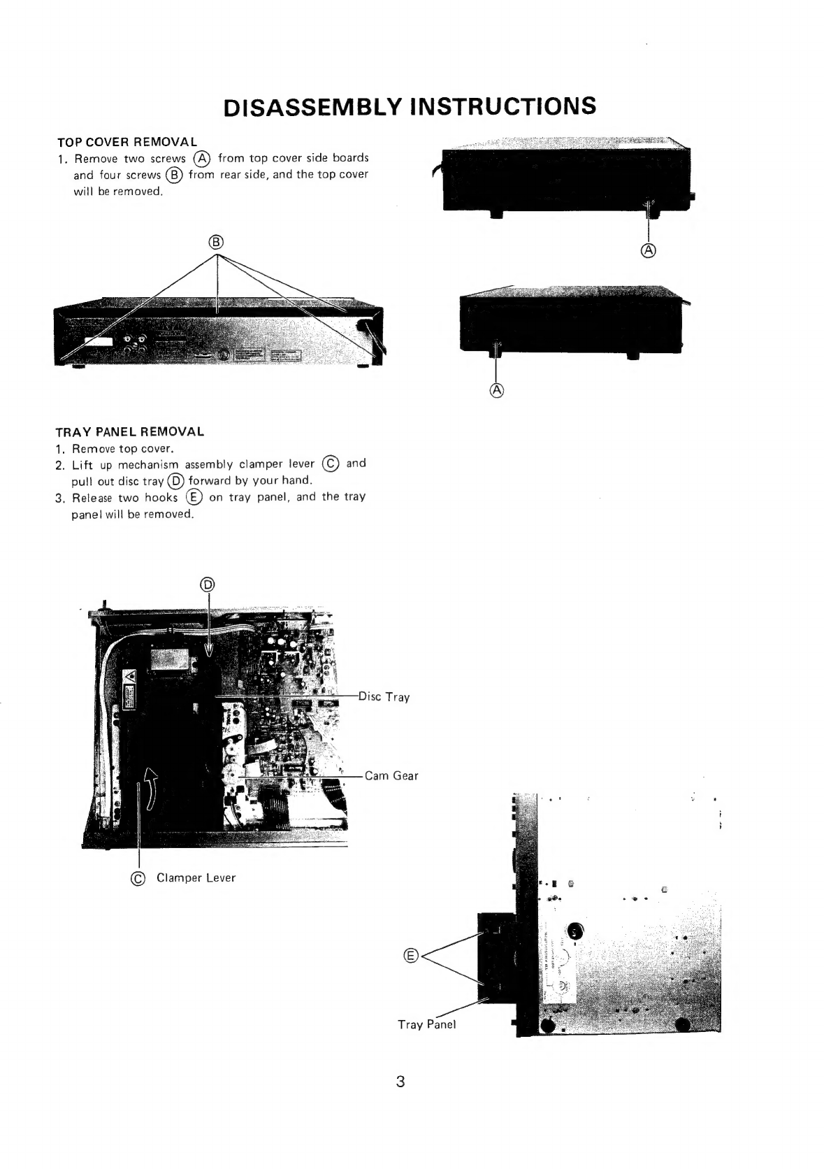
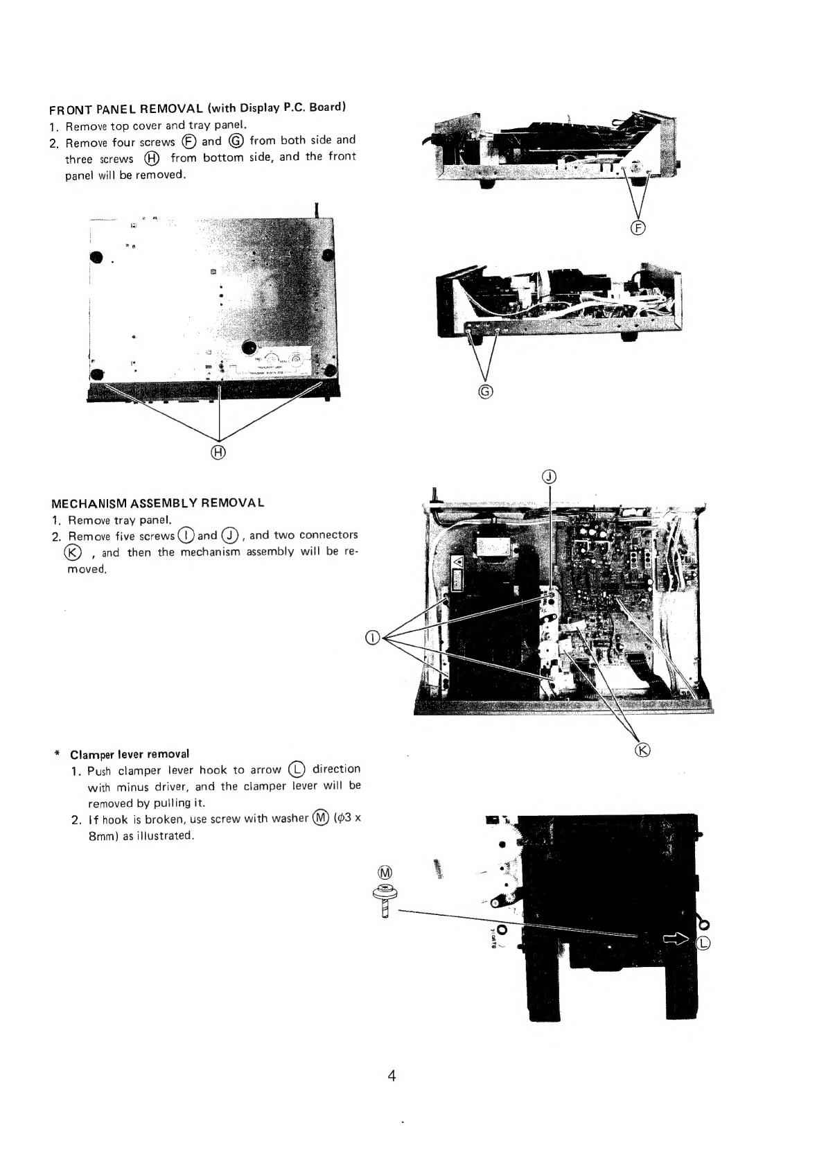
Table of contents
Other NAD CD Player manuals
NAD
NAD C 542 User manual
NAD C565BEE User manual
NAD C 546BEE User manual
NAD C 521BEE User manual
NAD 523 User manual
NAD 522 User manual
NAD 510 User manual
NAD C541 User manual
NAD C515BEE User manual
NAD 502 User manual
NAD C 516BEE User manual
NAD 5420 User manual
NAD C521 User manual
NAD C 521BEE Administrator Guide
NAD 517 User manual
NAD C521i User manual
NAD T 571 User manual
NAD 524 User manual
NAD Classic 512 User manual
RCA
RCA RP-7923 instruction manual
Pioneer
Pioneer DEH-P3550MP XM Operation manual
Philips
Philips AZ1207 owner's manual
Philips CD582 user manual
Philips AZ 6821 operating manual
Lasonic
Lasonic MSU-2020 user manual
THOMSON
THOMSON RCD150 user manual
Denon
Denon DCD-1420 Service manual
Panasonic
Panasonic SJ-MR100 operating instructions
Onkyo
Onkyo DX-7210 instruction manual
Sony
Sony MZ-R3 operating instructions
Denon DVM-4800 Service manual
JBL
JBL MR-32 Operation manual
RCA RCD152 Specifications
Technics
Technics SL-PS770A Service manual
Clarion
Clarion compact disc owner's manual
Sony MZ-M10 operating instructions
Philips Expanium AZ 1538 user manual