- 3 -
SERVICE SAFETY PRECAUTIONS
1. Replacing the fuses
CAUTION: FOR CONTINUED PROTECTION AGAINST THE RISK OF FIRE REPLACE ONLY WITH SAME TYPE
OF FUSE.
Reference No Part Number Description
FC201 *C 5120-0050+0 FUSE T1.6A/250V 5X20
FC201 *AH 5120-0052+0 FUSE T1.6A 250V 5X20
FC202, FC204, FC205 *C 5120-0018+0 FUSE T1A 250V 5X20
FC202, FC204, FC205 *AH 5120-0020+0 FU T1A 250V UL/CSA 5X20
FC203 *C 5120-0035+0 FU T100MA 250V
FC203 *AH 5120-0036+0 FUSE 250V 100MA T 5X20
NOTE:
<*AH > : USA, CANADIAN MODEL ONLY.
<*C > : EUROPEAN MODEL ONLY.
2. Safety check out
(Only U.S.A. model)
Before returning the product to the customer, make leakage current or resistance measurements to determine that
exposed parts are acceptably insulated from the supply circuit.
Parts marked with the symbol are critical with regard to the risk of fire and electric shock.
Replace only with parts recommended by the manufacturer.
CONTENTS
DESCRIPTION PAGE
SPECIFICATIONS . . . . . . . . . . . . . . . . . . . . . . . . . . . . . . . . . . . . . . . . . . . . . . . . . . . . . . . . . . . . . 4
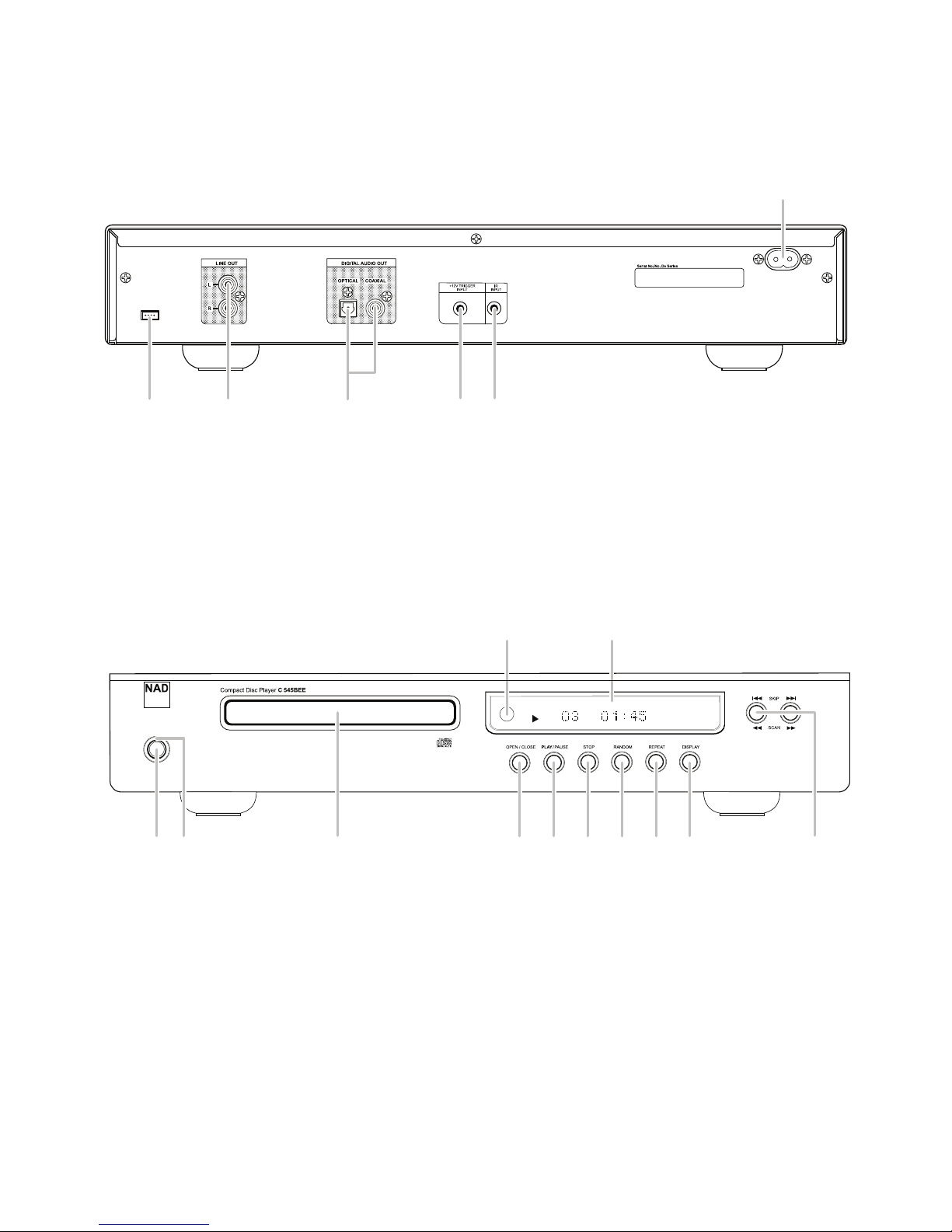
REAR PANEL / FRONT PANEL . . . . . . . . . . . . . . . . . . . . . . . . . . . . . . . . . . . . . . . . . . . . . . . . . . 5
DISASSEMBLY INSTRUCTIONS . . . . . . . . . . . . . . . . . . . . . . . . . . . . . . . . . . . . . . . . . . . . . . . . . 6
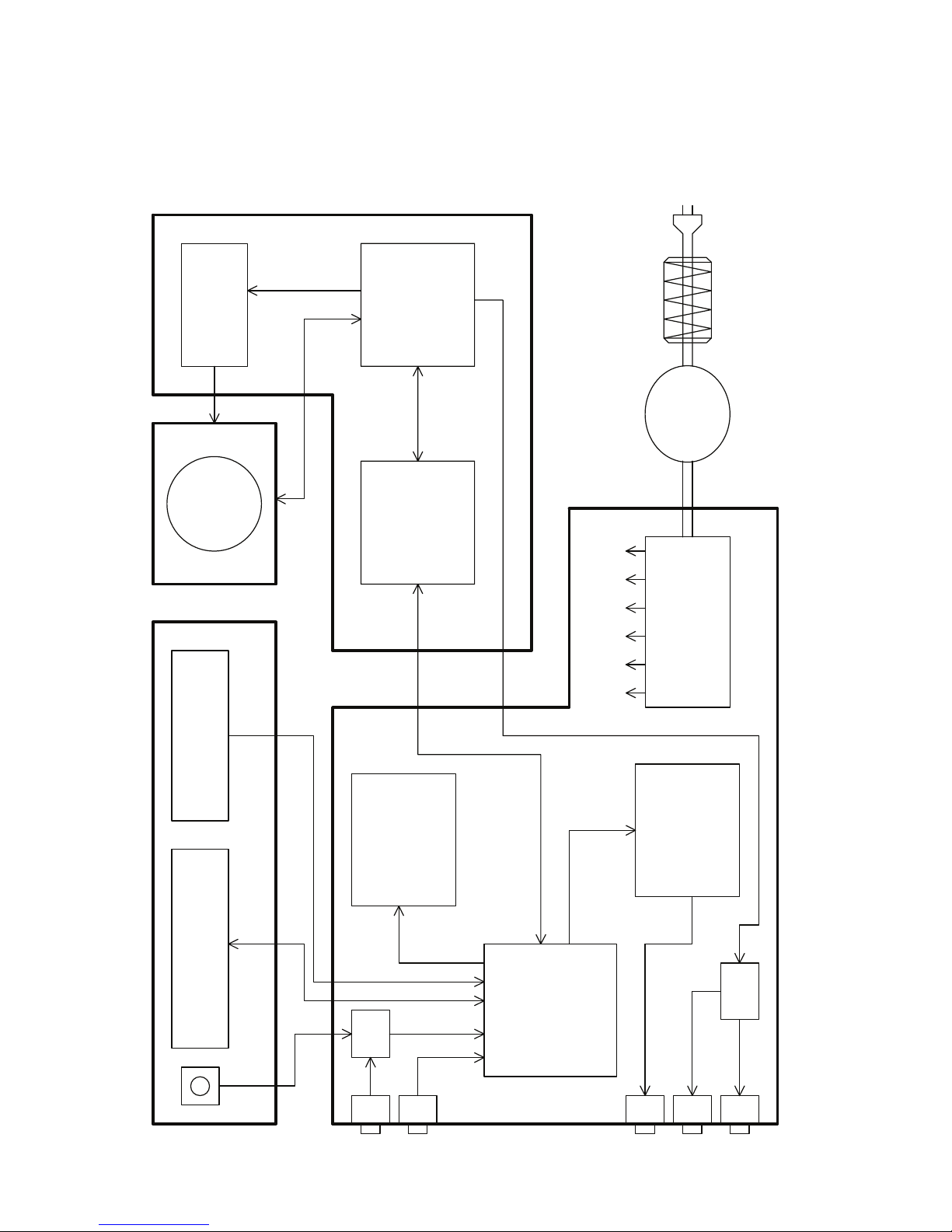
BLOCK DIAGRAM . . . . . . . . . . . . . . . . . . . . . . . . . . . . . . . . . . . . . . . . . . . . . . . . . . . . . . . . . . . . 7
WIRING DIAGRAM . . . . . . . . . . . . . . . . . . . . . . . . . . . . . . . . . . . . . . . . . . . . . . . . . . . . . . . . . . . . 8
RF PATTERN TESTING . . . . . . . . . . . . . . . . . . . . . . . . . . . . . . . . . . . . . . . . . . . . . . . . . . . . . . . . 9
IMPORTANT NOTES . . . . . . . . . . . . . . . . . . . . . . . . . . . . . . . . . . . . . . . . . . . . . . . . . . . . . . .10-12
PCB LAYOUT . . . . . . . . . . . . . . . . . . . . . . . . . . . . . . . . . . . . . . . . . . . . . . . . . . . . . . . . . . . . .13-16
SCHEMATIC DIAGRAM . . . . . . . . . . . . . . . . . . . . . . . . . . . . . . . . . . . . . . . . . . . . . . . . . . . . .17-23
IC BLOCK DIAGRAM . . . . . . . . . . . . . . . . . . . . . . . . . . . . . . . . . . . . . . . . . . . . . . . . . . . . . . .24-31
TROUBLESHOOTING GUIDE . . . . . . . . . . . . . . . . . . . . . . . . . . . . . . . . . . . . . . . . . . . . . . . . . . 32
ELECTRICAL PARTS LIST . . . . . . . . . . . . . . . . . . . . . . . . . . . . . . . . . . . . . . . . . . . . . . . . . . .33-44
MECHANISM EXPLODED VIEW . . . . . . . . . . . . . . . . . . . . . . . . . . . . . . . . . . . . . . . . . . . . . . . . 45
MECHANISM EXPLODED VIEW PARTS LIST . . . . . . . . . . . . . . . . . . . . . . . . . . . . . . . . . . . . . 46
EXPLODED VIEW . . . . . . . . . . . . . . . . . . . . . . . . . . . . . . . . . . . . . . . . . . . . . . . . . . . . . . . . . . . . 47
EXPLODED VIEW PARTS LIST . . . . . . . . . . . . . . . . . . . . . . . . . . . . . . . . . . . . . . . . . . . . . . . . . 48
PACKING DIAGRAM . . . . . . . . . . . . . . . . . . . . . . . . . . . . . . . . . . . . . . . . . . . . . . . . . . . . . . . . . . 49