7
CONTENTS
DESCRIPTION
PAGE
SPECIFICATIONS:
si
cesiccatadecstcaspasyausgeeh
nctiee
wes
5e
ag
ce
gelasaweitnas-aaeus
ta
raamg
naa
ddebeddagniaea
nraiebopnanteaeueniae
4
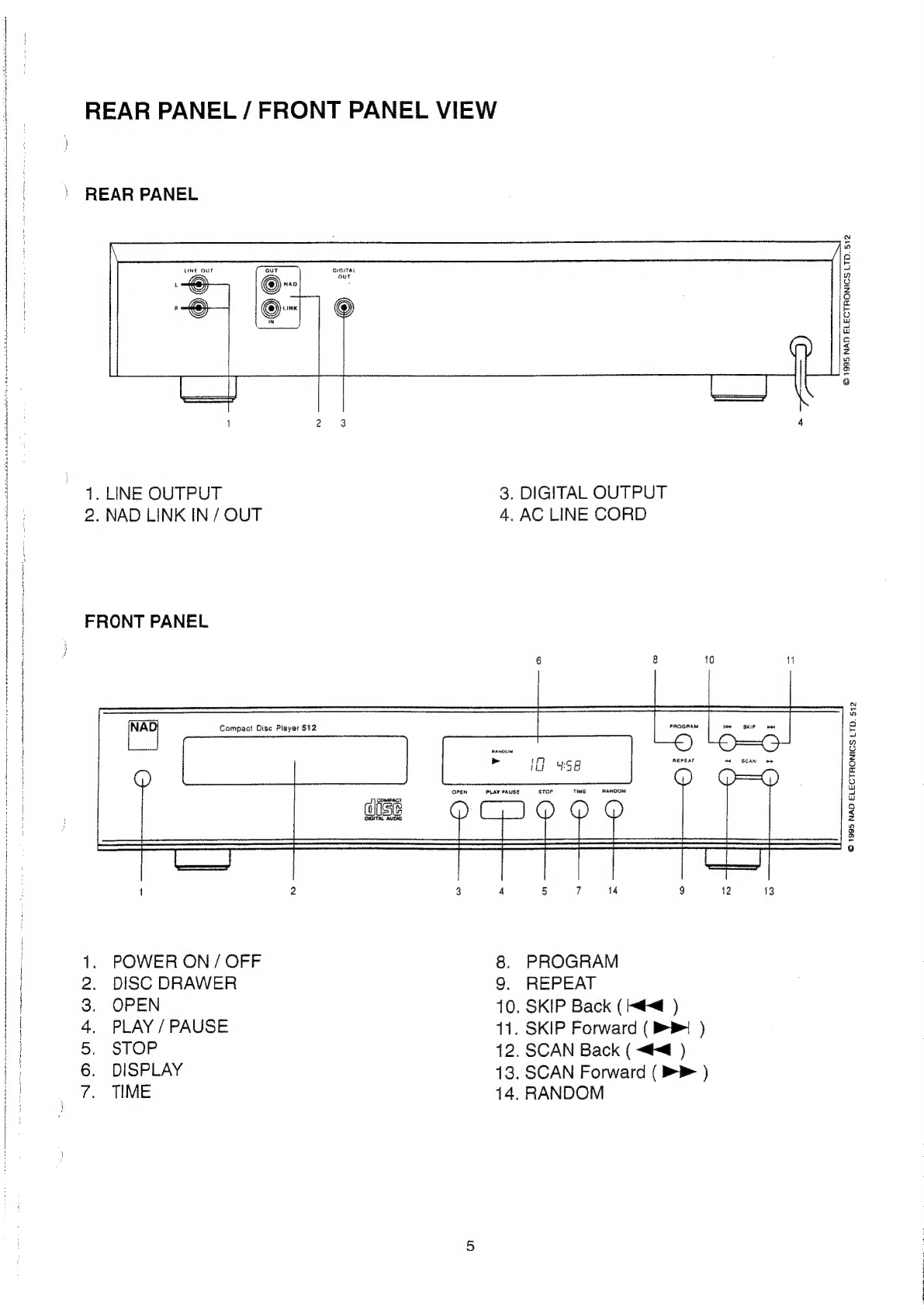
REAR:
PANEL?
FRONT
PANEL
VIEW
siicias
uct
anomie
ednesinctexeneasadie
Ga ar
cacuren
nurs
ane
5
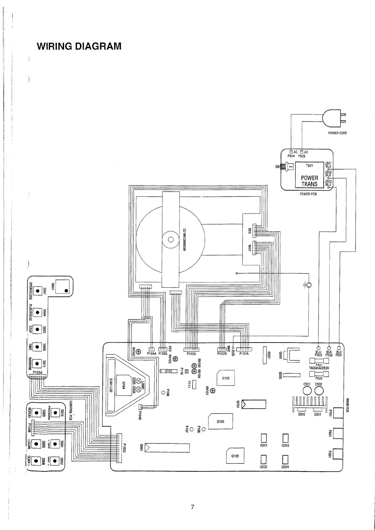
BOCK
DIAG
EAD
iiaslesia
duc
exiaute
copsetere
buak
a
ae
cay
Saananug
sa
vieiilneesealacearnia
vain
aeaniiney
tatalaahan
eatin
ieiad
taaiamenae
6
VEN
Ce
TAG
oc
occe
dctsin
So
sbeet
tcealagnmsesisa
utess
od
ed
vag
lenses
spe
qu
dusstaa
phaiavnedatanteusuauaaesnennera
sat
doaaieudnecie
ri
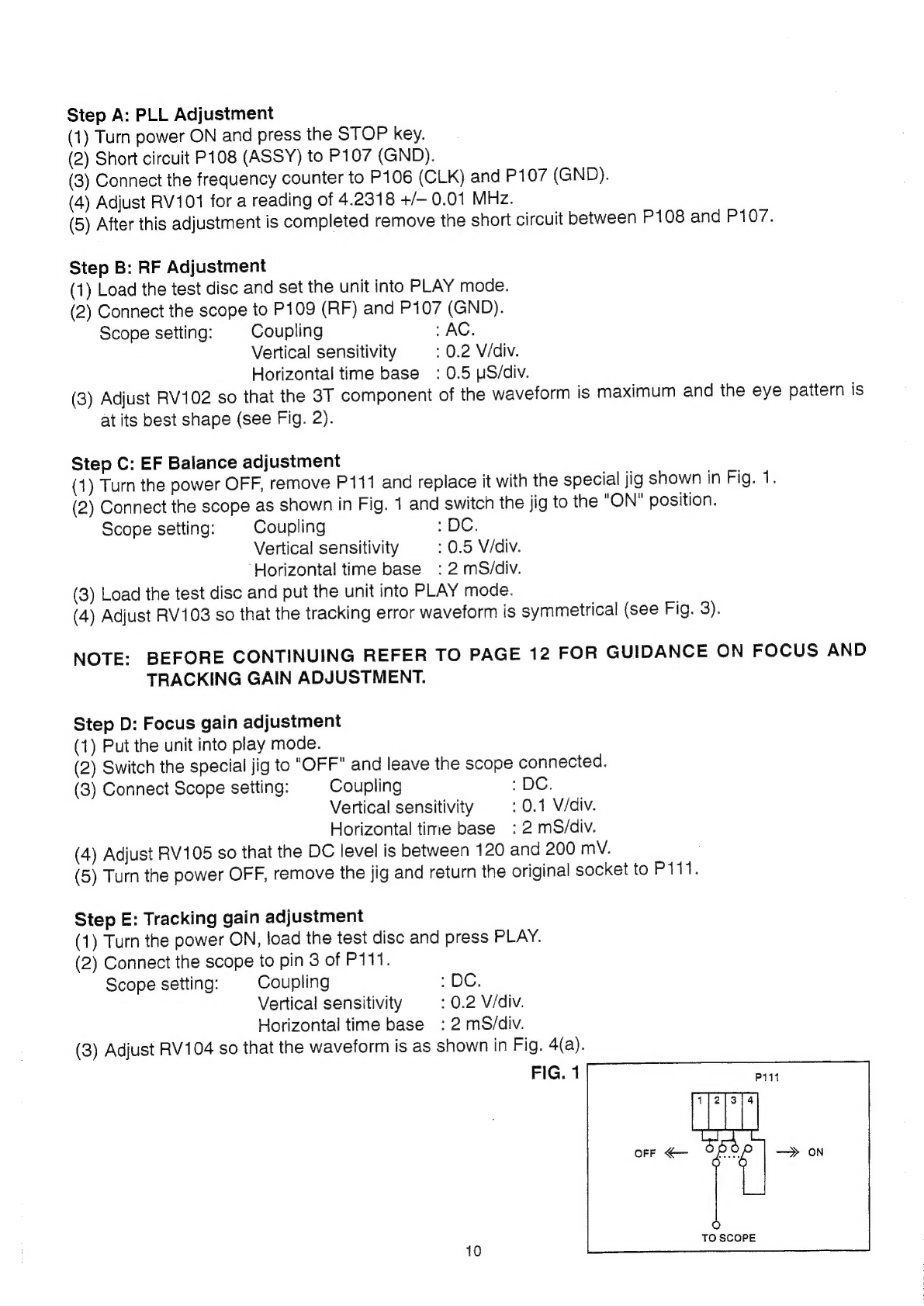
DISASSEMBLY
INS
TRUCTIONS
4
itsnkea
ieneoa
nese
ncaa
ee
ee
8
ADIGNMENT
PROCEDURE,
sisieicsetacaespenstrsdeaeuraiccantsg
nasntateapeatancuen
ned
lecumn
eaeieuatanscii
ssa
tuaus
pense
9-11
GUIDANCE
ON
FOCUS
AND
TRACKING
GAIN
ADJUSTMENT
...........::cecescsecerssessessseasseaeeenes
12
IM
PORTANT
NO
PES
ss
scncetesnSocrsnabeaaras
dues
wusscien
cri
sdnaceh
ctapaisieatoerpoveuselacdvagaasuvagaan
aes
betacatesaneagedaaes
13
-14
POBLAVOUT
(PARTS.
SIDE):
ocsssastociesecianckaciseatiNlanenevnelwteierenste
ardamrtiannucatecni
aime
1316
SCHEMATIC
DIAGRAM
swinsiy
Siscdunn
ros
tanientsssiadcesstecentaiteah
nos
vaesd
ease
tenoadstnsedsaninesseguan
anpanmanteasaracsiisdes
10718
IG
BLOCK
DIAGHAM
siceviccutcs
unasalon
tab
iieclne
taharaecupeaeseusies
uneatuaauie
ia
aacaataaiatntditagunly
elasccdaisbenecainte
19
-21
TROUBLESHOOTING:
GUIDE
co.
c.saeast.atun
sates
wticannausberouaiienesudstuneta
de
avadoGaaaatiatgel
usagi
ssvesiaadhcusaueccianeatial
22
EXPLODED
VIEW
cts,
iitesacateselosei.Geinerastuelsqade
cipluntinuctharks
esbantenupoieaas
aleve
deeduugandt
buleutenvatvaalatteneancs
23
EXPLODED:
VIEW
PARTS
UIST
icc
sciccnstesasnvinedautisaduen
ea
ciusasatecatinantsaanusiiran
diem
ectsaesselapnediedesiiriiaes
24
MECHANISM
EXPLODED
VIEW
een
earner
ron
era
ich
SraakestSeastiss
25
-27
BLECTRIGAL
PARAS
LIST
cccadeduccachcosstesientan
iamicouet
ceauiywaiaiaias
Shakin
nincon
nna
teuteebagnaadvieteange
28
-30
PACKING:
DIAGHAIWE
ssc:
chticninnaidarcetniacSeaie
cod
iuldscdatsincitvtieatemeavautinadac
iar
etieey
cadens
idvaeuneatigvedmendeces
31