National Instruments sbRIO-9651 User manual

376963A-01 Oct14
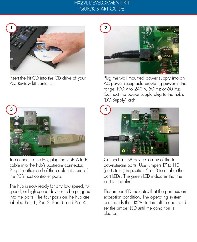
3.3 V PWR IN
Reference Carrier Board
sbRIO-9651 SOM
Refer to the NI Trademarks and Logo Guidelines at ni.com/trademarks for information on National Instruments trademarks. Other product and company names mentioned herein are trademarks or trade names of
their respective companies. For patents covering National Instruments products/technology, refer to the appropriate location: Help»Patents in your software, the patents.txt file on your media, or the National
Instruments Patent Notice at ni.com/patents.You can find information about end-user license agreements (EULAs) and third-party legal notices in the readme file for your NI product. Refer to the Export Compliance
Information at ni.com/legal/export-compliance for the National Instruments global trade compliance policy and how to obtain relevant HTS codes, ECCNs, and other import/export data. NI MAKES NO EXPRESS
OR IMPLIED WARRANTIES AS TO THE ACCURACY OF THE INFORMATION CONTAINED HEREIN AND SHALL NOT BE LIABLE FOR ANY ERRORS. U.S. Government Customers: The data contained in this manual
was developed at private expense and is subject to the applicable limited rights and restricted data rights as set forth in FAR 52.227-14, DFAR 252.227-7014, and DFAR 252.227-7015.
© 2014 National Instruments. All rights reserved. Printed in Hungary.
QUICK START GUIDE
NI sbRIO-9651
System on Module Development Kit
The NI sbRIO-9651 System on Module (SOM) development kit includes the sbRIO-9651 SOM and a reference carrier board. Use this document to
help you get started with setting up the system and reviewing an example LabVIEW project.
Parts Locator Diagram
Block Diagram
The following gure shows the connections and interfaces between the sbRIO-9651 SOM and the
reference carrier board.
Getting Started with the sbRIO-9651 SOM Development Kit
Complete the following steps to get started with the sbRIO-9651 SOM and the reference carrier board, including setting up your hardware and
reviewing an example LabVIEW project that includes an sbRIO-9651 SOM target.
Note Refer to the documentation listed in the Where to Go Next section of this document for additional sbRIO-9651 SOM resources.
1 Installing Required Software
Install or verify that you have installed the following software:
• LabVIEW 2014 or later
• LabVIEW Real-Time Module 2014 or later
• LabVIEW FPGA Module 2014 or later
• NI-RIO Device Drivers August 2014 or later
2 Connecting Power
a. Ensure that your included 12 V power supply is disconnected
from an AC power source.
b. Connect the power supply to the Power (9 V–16 V) terminal
on the reference carrier board.
c. Plug in the power supply to the AC power source.
3 Connecting to a Computer
To connect with USB:
a. Connect one end of the included USB cable to the
USB0 Device port on the reference carrier board.
b. Connect the other end of the USB cable to a computer.
To connect with Ethernet:
a. Connect a standard Category 5 (CAT-5) or better Ethernet
cable to the Ethernet0 port on the reference carrier board.
b. Connect the other end of the Ethernet cable to an Ethernet hub
or to a computer.
When you power up the device, it attempts to initiate a DHCP
network connection. If the device cannot initiate a DHCP
connection, it connects to the network with a link-local IP
address with the form 169.254.x.x.
c. In Measurement & Automation Explorer (MAX), congure
network settings for the device. Refer to the MAX Help for
CompactRIO and Single-Board RIO for more information
about conguring network settings in MAX.
4 Reviewing Example Software
a. In LabVIEW, open the sbRIO-9651 SOM reference
carrier board example project, located at \labview\
examples\CompactRIO\Chassis Specific\
sbRIO-9651 CRB Getting Started\
sbRIO-9651 CRB Getting Started.lvproj.
b. Expand the sbRIO-9651 Socket (DevKit) item and
review the LabVIEW FPGA I/O items dened for the
sbRIO-9651 SOM development kit.
Note The socketed component-level IP (CLIP) for
the reference carrier board, located at <National
Instruments>\shared\CompactRIO\CLIPs\
sbRIO-9651\DevKit\DevKit.cfg, denes the
I/O conguration used in this application. When you
are ready to create a carrier board for your own
application, you can use the development kit CLIP
denition as a starting point for a new CLIP.
c. Open the sbRIO-9651 CRB Getting Started.vi le
in the project and review the block diagram.
d. Compile the VI and download it to the ash memory of the
sbRIO-9651 SOM. Refer to the Downloading an FPGA VI to
the Flash Memory of an FPGA Target topic in the LabVIEW
Help (FPGA Module) for more information.
Note When you create your own CLIP and dene
processor peripherals (such as secondary Ethernet,
CAN, or additional serial ports), you must compile
your FPGA VI and download it to the ash of the
sbRIO-9651 SOM. This ensures that the driver for the
peripheral can load properly at boot time.
J1 8 × 40 320-Pin Connector
CPLD RTC USB
PHY
USB
PHY
Reset In/Out
VBAT
USB1 HOST
USB0
TX/RX Serial
16 LVTTL SE
VIO BANK 2
VIO BANK 3
24 Diff/48 SE
24 Diff/48 SE
VIO BANK 1
SDIO
GigE
PHY
GMII
GigE Pairs
DDR3
NAND
MIO
Bank 3
Bank 2
Bank 1
Bank 0
DDR
Zynq-7020
CLG484
Reset Button
USB0 Device
USB1 Host
Ethernet0
Ethernet1
RS-232 Port 1
RS-232 Port 2
RS-485 Port 3
CAN0
Bank 3 DIO
5x Pmod
Power
1 sbRIO-9651 SOM
2 User Buttons
3 SDHC Slot
4 LEDs
5 Reset Button
6 VIO_BANK3 Voltage Selection Jumper
7 Ethernet0 Port
8 Ethernet1 Port
9 USB0 Device Port
10 RTC Battery
11 USB1 Host Port
12 Power Connector (9 V–16 V)
13 Pmod Connector 5 (I2C)
14 Pmod Connectors 1 through 4
15 Bank 3 FPGA I/O
16 Prototyping Area
17 RS-232 Port 1 (Console Out)
18 RS-232 Port 2
19 RS-485 Port 5
20 CAN0 Port
13
20
19
18
16
17
7
8
9
11
10
12
13
15
15
5
14
6
24
Legend
Fixed behavior signals
User-defined FPGA signals
Power signals
Internal
Power
Rails
Internal
Power
Rails
1.8 V PS 1.5 V PS 1.2 V PS 1.0 V PS
Where to Go Next
Refer to the following additional resources as you design, prototype, and implement your sbRIO-9651 SOM application.
NI sbRIO-9651 System on Module
OEMDeviceSpecications—Device
and peripheral requirements for the
sbRIO-9651 SOM.
NI sbRIO-9651 System on Module
Carrier Board Design Guide—
Recommendations and constraints for
designing a custom carrier board.
LabVIEW Help—Information about
conguring sbRIO-9651 SOM targets in
LabVIEW and compiling, downloading,
and running FPGA VIs.
NI Single-Board RIO CLIP Generator
Help—Reference for the sbRIO CLIP
Generator application.
ni.com/singleboard/setup—
Tutorials, demos, and videos for getting
started with NI sbRIO devices.
ni.com/training—Online or
classroom training and certications.
ni.com/support—Discussion
forums, example code, and other helpful
resources.
Legend
PDF located at ni.com/manuals
Help available in-product
Online at ni.com
GigE PHY
XCVR
XCVR
XCVR
XCVR
3.3 V PS
5.0 V PS
1.2 V PS 2.5 V PS VIO_BANK3 ADJ PS
sbRIO-9651 Interface Connector
(Molex part number 45970-4130)
24 Diff/48 SE
FPGA_CFG
376963A-01 Oct14
3.3 V PWR IN
Reference Carrier Board
sbRIO-9651 SOM
Refer to the NI Trademarks and Logo Guidelines at ni.com/trademarks for information on National Instruments trademarks. Other product and company names mentioned herein are trademarks or trade names of
their respective companies. For patents covering National Instruments products/technology, refer to the appropriate location: Help»Patents in your software, the patents.txt file on your media, or the National
Instruments Patent Notice at ni.com/patents.You can find information about end-user license agreements (EULAs) and third-party legal notices in the readme file for your NI product. Refer to the Export Compliance
Information at ni.com/legal/export-compliance for the National Instruments global trade compliance policy and how to obtain relevant HTS codes, ECCNs, and other import/export data. NI MAKES NO EXPRESS
OR IMPLIED WARRANTIES AS TO THE ACCURACY OF THE INFORMATION CONTAINED HEREIN AND SHALL NOT BE LIABLE FOR ANY ERRORS. U.S. Government Customers: The data contained in this manual
was developed at private expense and is subject to the applicable limited rights and restricted data rights as set forth in FAR 52.227-14, DFAR 252.227-7014, and DFAR 252.227-7015.
© 2014 National Instruments. All rights reserved.
QUICK START GUIDE
NI sbRIO-9651
System on Module Development Kit
The NI sbRIO-9651 System on Module (SOM) development kit includes the sbRIO-9651 SOM and a reference carrier board. Use this document to
help you get started with setting up the system and reviewing an example LabVIEW project.
Parts Locator Diagram
Block Diagram
The following gure shows the connections and interfaces between the sbRIO-9651 SOM and the
reference carrier board.
Getting Started with the sbRIO-9651 SOM Development Kit
Complete the following steps to get started with the sbRIO-9651 SOM and the reference carrier board, including setting up your hardware and
reviewing an example LabVIEW project that includes an sbRIO-9651 SOM target.
Note Refer to the documentation listed in the Where to Go Next section of this document for additional sbRIO-9651 SOM resources.
1 Installing Required Software
Install or verify that you have installed the following software:
• LabVIEW 2014 or later
• LabVIEW Real-Time Module 2014 or later
• LabVIEW FPGA Module 2014 or later
• NI-RIO Device Drivers August 2014 or later
2 Connecting Power
a. Ensure that your included 12 V power supply is disconnected
from an AC power source.
b. Connect the power supply to the Power (9 V–16 V) terminal
on the reference carrier board.
c. Plug in the power supply to the AC power source.
3 Connecting to a Computer
To connect with USB:
a. Connect one end of the included USB cable to the
USB0 Device port on the reference carrier board.
b. Connect the other end of the USB cable to a computer.
To connect with Ethernet:
a. Connect a standard Category 5 (CAT-5) or better Ethernet
cable to the Ethernet0 port on the reference carrier board.
b. Connect the other end of the Ethernet cable to an Ethernet hub
or to a computer.
When you power up the device, it attempts to initiate a DHCP
network connection. If the device cannot initiate a DHCP
connection, it connects to the network with a link-local IP
address with the form 169.254.x.x.
c. In Measurement & Automation Explorer (MAX), congure
network settings for the device. Refer to the MAX Help for
CompactRIO and Single-Board RIO for more information
about conguring network settings in MAX.
4 Reviewing Example Software
a. In LabVIEW, open the sbRIO-9651 SOM reference
carrier board example project, located at \labview\
examples\CompactRIO\Chassis Specific\
sbRIO-9651 CRB Getting Started\
sbRIO-9651 CRB Getting Started.lvproj.
b. Expand the sbRIO-9651 Socket (DevKit) item and
review the LabVIEW FPGA I/O items dened for the
sbRIO-9651 SOM development kit.
Note The socketed component-level IP (CLIP) for
the reference carrier board, located at <National
Instruments>\shared\CompactRIO\CLIPs\
sbRIO-9651\DevKit\DevKit.cfg, denes the
I/O conguration used in this application. When you
are ready to create a carrier board for your own
application, you can use the development kit CLIP
denition as a starting point for a new CLIP.
c. Open the sbRIO-9651 CRB Getting Started.vi le
in the project and review the block diagram.
d. Compile the VI and download it to the ash memory of the
sbRIO-9651 SOM. Refer to the Downloading an FPGA VI to
the Flash Memory of an FPGA Target topic in the LabVIEW
Help (FPGA Module) for more information.
Note When you create your own CLIP and dene
processor peripherals (such as secondary Ethernet,
CAN, or additional serial ports), you must compile
your FPGA VI and download it to the ash of the
sbRIO-9651 SOM. This ensures that the driver for the
peripheral can load properly at boot time.
J1 8 × 40 320-Pin Connector
CPLD RTC USB
PHY
USB
PHY
Reset In/Out
VBAT
USB1 HOST
USB0
TX/RX Serial
16 LVTTL SE
VIO BANK 2
VIO BANK 3
24 Diff/48 SE
24 Diff/48 SE
VIO BANK 1
SDIO
GigE
PHY
GMII
GigE Pairs
DDR3
NAND
MIO
Bank 3
Bank 2
Bank 1
Bank 0
DDR
Zynq-7020
CLG484
Reset Button
USB0 Device
USB1 Host
Ethernet0
Ethernet1
RS-232 Port 1
RS-232 Port 2
RS-485 Port 3
CAN0
Bank 3 DIO
5x Pmod
Power
1 sbRIO-9651 SOM
2 User Buttons
3 SDHC Slot
4 LEDs
5 Reset Button
6 VIO_BANK3 Voltage Selection Jumper
7 Ethernet0 Port
8 Ethernet1 Port
9 USB0 Device Port
10 RTC Battery
11 USB1 Host Port
12 Power Connector (9 V–16 V)
13 Pmod Connector 5 (I2C)
14 Pmod Connectors 1 through 4
15 Bank 3 FPGA I/O
16 Prototyping Area
17 RS-232 Port 1 (Console Out)
18 RS-232 Port 2
19 RS-485 Port 5
20 CAN0 Port
13
20
19
18
16
17
7
8
9
11
10
12
13
15
15
5
14
6
24
Legend
Fixed behavior signals
User-defined FPGA signals
Power signals
Internal
Power
Rails
Internal
Power
Rails
1.8 V PS 1.5 V PS 1.2 V PS 1.0 V PS
Where to Go Next
Refer to the following additional resources as you design, prototype, and implement your sbRIO-9651 SOM application.
NI sbRIO-9651 System on Module
OEMDeviceSpecications—Device
and peripheral requirements for the
sbRIO-9651 SOM.
NI sbRIO-9651 System on Module
Carrier Board Design Guide—
Recommendations and constraints for
designing a custom carrier board.
LabVIEW Help—Information about
conguring sbRIO-9651 SOM targets in
LabVIEW and compiling, downloading,
and running FPGA VIs.
NI Single-Board RIO CLIP Generator
Help—Reference for the sbRIO CLIP
Generator application.
ni.com/singleboard/setup—
Tutorials, demos, and videos for getting
started with NI sbRIO devices.
ni.com/training—Online or
classroom training and certications.
ni.com/support—Discussion
forums, example code, and other helpful
resources.
Legend
PDF located at ni.com/manuals
Help available in-product
Online at ni.com
GigE PHY
XCVR
XCVR
XCVR
XCVR
3.3 V PS
5.0 V PS
1.2 V PS 2.5 V PS VIO_BANK3 ADJ PS
sbRIO-9651 Interface Connector
(Molex part number 45970-4130)
24 Diff/48 SE
FPGA_CFG
Other manuals for sbRIO-9651
1
Other National Instruments Microcontroller manuals
Popular Microcontroller manuals by other brands

Samsung
Samsung ARTIK 053s Hardware user's guide

Freescale Semiconductor
Freescale Semiconductor MCF5282 User guide addendum

Dialog Semiconductor
Dialog Semiconductor DA1468 series user manual

Epson
Epson S1C17001 Technical manual

New Micros
New Micros TiniARM user manual

Infineon
Infineon XMC4000 series Board User's Manual

NXP Semiconductors
NXP Semiconductors LPC-Link2 Wiring diagram

Renesas
Renesas RL78 Series user manual

Arduino
Arduino Portenta H7 Lite Product reference manual

Texas Instruments
Texas Instruments CC2520EM quick start guide

Dialog Semiconductor
Dialog Semiconductor SmartBond DA14585 user manual

Cypress
Cypress CY8CKIT-046 quick start guide